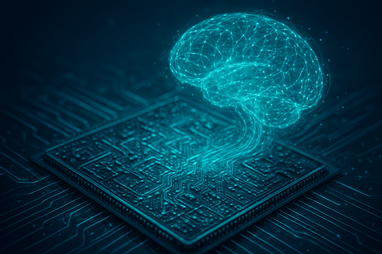
In a groundbreaking era of artificial intelligence, a revolutionary computing paradigm known as neuromorphic computing is rapidly gaining prominence, promising to redefine the very foundations of how machines learn, process information, and interact with the world. Drawing profound inspiration from the human brain's intricate structure and functionality, this technology is moving far beyond its initial applications in self-driving cars, poised to unlock unprecedented levels of energy efficiency, real-time adaptability, and cognitive capabilities across a vast spectrum of industries. As the conventional Von Neumann architecture increasingly strains under the demands of modern AI, neuromorphic computing emerges as a pivotal solution, heralding a future of smarter, more sustainable, and truly intelligent machines.
Technical Leaps: Unpacking the Brain-Inspired Hardware and Software
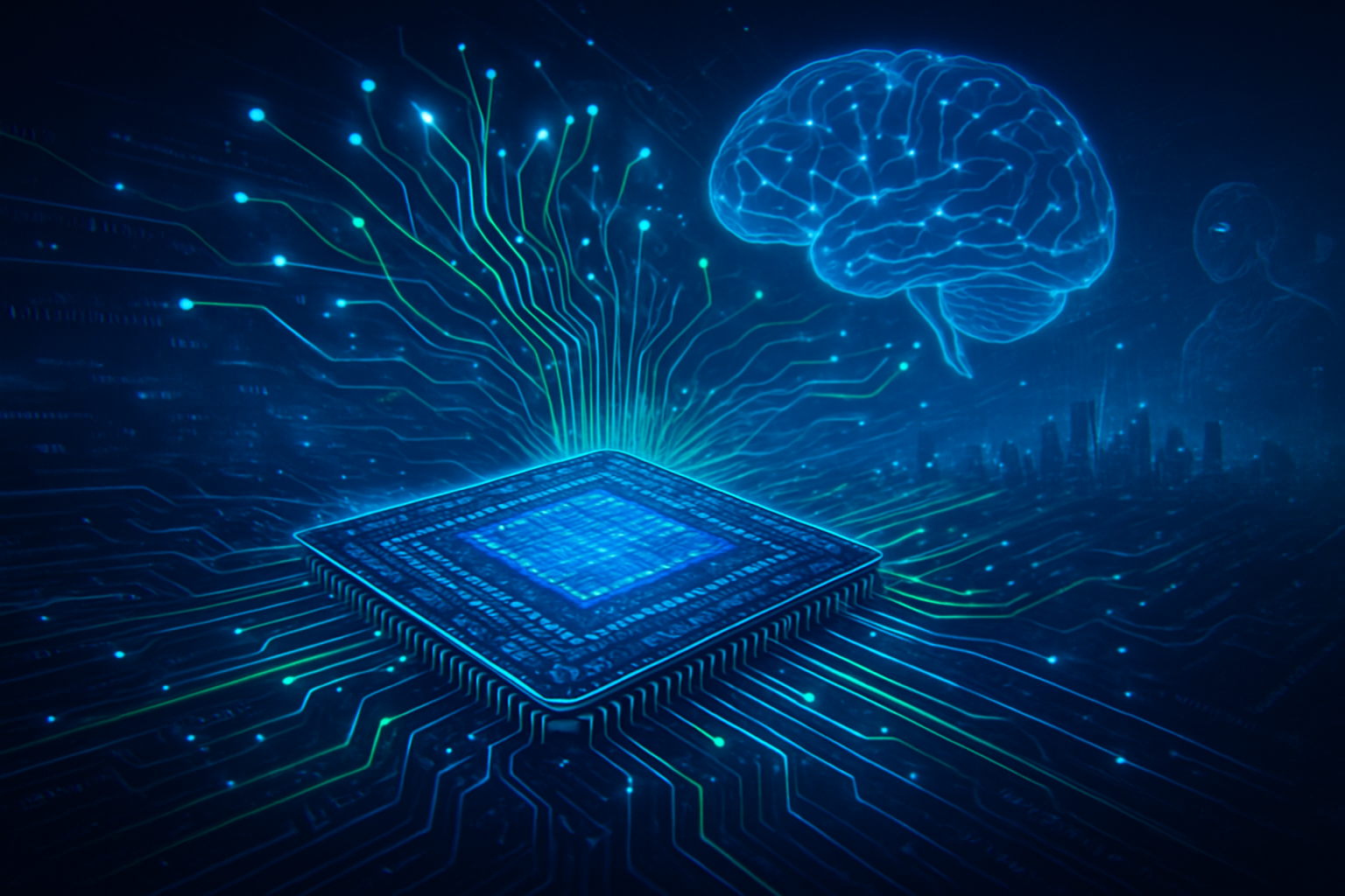
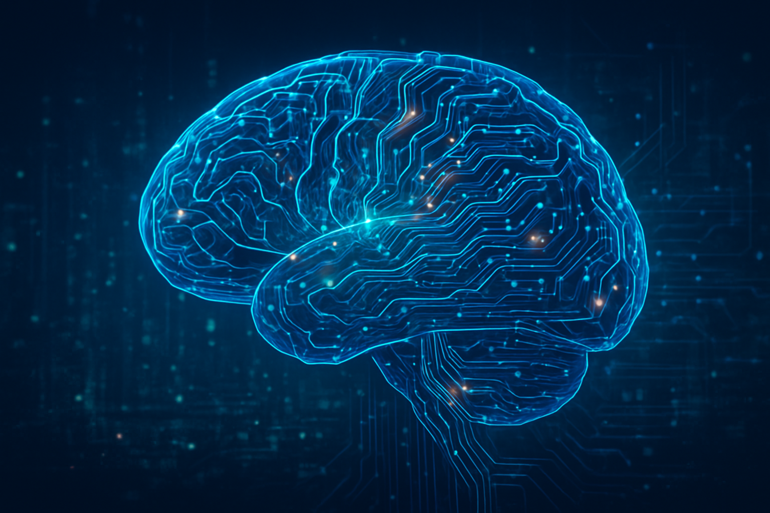
Neuromorphic architectures represent a radical departure from traditional computing, fundamentally rethinking how processing and memory interact. Unlike the Von Neumann architecture, which separates the CPU and memory, leading to the infamous "Von Neumann bottleneck," neuromorphic chips integrate these functions directly within artificial neurons and synapses. This allows for massively parallel, event-driven processing, mirroring the brain's efficient communication through discrete electrical "spikes."
Leading the charge in hardware innovation are several key players. Intel (NASDAQ: INTC) has been a significant force with its Loihi series. The original Loihi chip, introduced in 2017, demonstrated a thousand-fold improvement in efficiency for certain neural networks. Its successor, Loihi 2 (released in 2021), advanced with 1 million artificial neurons and 120 million synapses, optimizing for scale, speed, and efficiency using spiking neural networks (SNNs). Most notably, in 2024, Intel unveiled Hala Point, the world's largest neuromorphic system, boasting an astounding 1.15 billion neurons and 128 billion synapses across 1,152 Loihi 2 processors. Deployed at Sandia National Laboratories, Hala Point is showcasing significant efficiency gains for robotics, healthcare, and IoT applications, processing signals 20 times faster than a human brain for some tasks.
IBM (NYSE: IBM) has also made substantial contributions with its TrueNorth chip, an early neuromorphic processor accommodating 1 million programmable neurons and 256 million synapses with remarkable energy efficiency (70 milliwatts). In 2023, IBM introduced NorthPole, a chip designed for highly efficient artificial neural network inference, claiming 25 times more energy efficiency and 22 times faster performance than NVIDIA's V100 GPU for specific inference tasks.
Other notable hardware innovators include BrainChip (ASX: BRN) with its Akida neuromorphic processor, an ultra-low-power, event-driven chip optimized for edge AI inference and learning. The University of Manchester's SpiNNaker (Spiking Neural Network Architecture) and its successor SpiNNaker 2 are million-core supercomputers designed to simulate billions of neurons. Heidelberg University's BrainScaleS-2 and Stanford University's Neurogrid also contribute to the diverse landscape of neuromorphic hardware. Startups like SynSense and Innatera are developing ultra-low-power, event-driven processors for real-time AI. Furthermore, advancements extend to event-based sensors, such as Prophesee's Metavision, which only activate upon detecting changes, leading to high temporal resolution and extreme energy efficiency.
Software innovations are equally critical, albeit still maturing. The core computational model is the Spiking Neural Network (SNN), which encodes information in the timing and frequency of spikes, drastically reducing computational overhead. New training paradigms are emerging, as traditional backpropagation doesn't directly translate to spike-based systems. Open-source frameworks like BindsNET, Norse, Rockpool, snnTorch, Spyx, and SpikingJelly are facilitating SNN simulation and training, often leveraging existing deep learning infrastructures like PyTorch.
The AI research community and industry experts have expressed "overwhelming positivity" towards neuromorphic computing, viewing it as a "breakthrough year" as the technology transitions from academia to tangible commercial products. While optimism abounds regarding its energy efficiency and real-time AI capabilities, challenges remain, including immature software ecosystems, the need for standardized tools, and proving a clear value proposition against established GPU solutions for mainstream applications. Some current neuromorphic processors still face latency and scalability issues, leading to a debate on whether they will remain niche or become a mainstream alternative, particularly for the "extreme edge" segment.
Corporate Chessboard: Beneficiaries, Disruptors, and Strategic Plays
Neuromorphic computing is poised to fundamentally reshape the competitive landscape for AI companies, tech giants, and startups, creating a new arena for innovation and strategic advantage. Its inherent benefits in energy efficiency, real-time processing, and adaptive learning are driving a strategic pivot across the industry.
Tech giants are heavily invested in neuromorphic computing, viewing it as a critical area for future AI leadership. Intel (NASDAQ: INTC), through its Intel Neuromorphic Research Community (INRC) and the recent launch of Hala Point, is positioning itself as a leader in large-scale neuromorphic systems. These efforts are not just about research; they aim to deliver significant efficiency gains for demanding AI applications in robotics, healthcare, and IoT, potentially reducing power consumption by orders of magnitude compared to traditional processors. IBM (NYSE: IBM) continues its pioneering work with TrueNorth and NorthPole, focusing on developing highly efficient AI inference engines that push the boundaries of performance per watt. Qualcomm (NASDAQ: QCOM) is developing its Zeroth platform, a brain-inspired computing architecture for mobile devices, robotics, and wearables, aiming to enable advanced AI operations directly on the device, reducing cloud dependency and enhancing privacy. Samsung is also heavily invested, exploring specialized processors and integrated memory solutions. These companies are engaged in a competitive race to develop neuromorphic chips with specialized architectures, focusing on energy efficiency, real-time learning, and robust hardware-software co-design for a new generation of AI applications.
Startups are finding fertile ground in this emerging field, often focusing on niche market opportunities. BrainChip (ASX: BRN) is a pioneer with its Akida neuromorphic processor, targeting ultra-low-power edge AI inference and learning, especially for smart cameras and IoT devices. GrAI Matter Labs develops brain-inspired AI processors for edge applications, emphasizing ultra-low latency for machine vision in robotics and AR/VR. Innatera Nanosystems specializes in ultra-low-power analog neuromorphic processors for advanced cognitive applications, while SynSense focuses on neuromorphic sensing and computing solutions for real-time AI. Other innovative startups include MemComputing, Rain.AI, Opteran, Aspirare Semi, Vivum Computing, and General Vision Inc., all aiming to disrupt the market with unique approaches to brain-inspired computing.
The competitive implications are profound. Neuromorphic computing is emerging as a disruptive force to the traditional GPU-dominated AI hardware market. While GPUs from companies like NVIDIA (NASDAQ: NVDA) are powerful, their energy intensity is a growing concern. The rise of neuromorphic computing could prompt these tech giants to strategically pivot towards specialized AI silicon or acquire neuromorphic expertise. Companies that successfully integrate neuromorphic computing stand to gain significant strategic advantages through superior energy efficiency, real-time decision-making, enhanced data privacy and security (due to on-chip learning), and inherent robustness. However, challenges remain, including the current decreased accuracy when converting deep neural networks to spiking neural networks, a lack of benchmarks, limited accessibility, and emerging cybersecurity threats like neuromorphic mimicry attacks (NMAs).
A Broader Canvas: AI Landscape, Ethics, and Historical Echoes
Neuromorphic computing represents more than just an incremental improvement; it's a fundamental paradigm shift that is reshaping the broader AI landscape. By moving beyond the traditional Von Neumann architecture, which separates processing and memory, neuromorphic systems inherently address the "Von Neumann bottleneck," a critical limitation for modern AI workloads. This brain-inspired design, utilizing artificial neurons and synapses that communicate via "spikes," promises unprecedented energy efficiency, processing speed, and real-time adaptability—qualities that are increasingly vital as AI models grow in complexity and computational demand.
Its alignment with current AI trends is clear. As deep learning models become increasingly energy-intensive, neuromorphic computing offers a sustainable path forward, potentially reducing power consumption by orders of magnitude. This efficiency is crucial for the widespread deployment of AI in power-constrained edge devices and for mitigating the environmental impact of large-scale AI computations. Furthermore, its ability for on-chip, real-time learning and adaptation directly addresses the limitations of traditional AI, which often requires extensive offline retraining on massive, labeled datasets.
However, this transformative technology also brings significant societal and ethical considerations. The ability of neuromorphic systems to learn and make autonomous decisions raises critical questions about accountability, particularly in applications like autonomous vehicles and environmental management. Like traditional AI, neuromorphic systems are susceptible to algorithmic bias if trained on flawed data, necessitating robust frameworks for explainability and transparency. Privacy and security are paramount, as these systems will process vast amounts of data, making compliance with data protection regulations crucial. The complex nature of neuromorphic chips also introduces new vulnerabilities, requiring advanced defense mechanisms against potential breaches and novel attack vectors. On a deeper philosophical level, the development of machines that can mimic human cognitive functions so closely prompts profound questions about human-machine interaction, consciousness, and even the legal status of highly advanced AI.
Compared to previous AI milestones, neuromorphic computing stands out as a foundational infrastructural shift. While breakthroughs in deep learning and specialized AI accelerators transformed the field by enabling powerful pattern recognition, neuromorphic computing offers a new computational substrate. It moves beyond the energy crisis of current AI by providing significantly higher energy efficiency and enables real-time, adaptive learning with smaller datasets—a capability vital for autonomous and personalized AI that continuously learns and evolves. This shift is akin to the advent of specialized AI accelerators, providing a new hardware foundation upon which the next generation of algorithmic breakthroughs can be built, pushing the boundaries of what machines can learn and achieve.
The Horizon: Future Trajectories and Expert Predictions
The future of neuromorphic computing is brimming with potential, with both near-term and long-term advancements poised to revolutionize artificial intelligence and computation. Experts anticipate a rapid evolution, driven by continued innovation in hardware, software, and a growing understanding of biological intelligence.
In the near term (1-5 years, extending to 2030), the most prominent development will be the widespread proliferation of neuromorphic chips in edge AI and Internet of Things (IoT) devices. This includes smart home systems, drones, robots, and various sensors, enabling localized, real-time data processing with enhanced AI capabilities, crucial for resource-constrained environments. Hardware will continue to improve with cutting-edge materials and architectures, including the integration of memristive devices that mimic synaptic connections for even lower power consumption. The development of spintronic devices is also expected to contribute to significant power reduction and faster switching speeds, potentially enabling truly neuromorphic AI hardware by 2030.
Looking further into the long term (beyond 2030), the vision for neuromorphic computing includes achieving truly cognitive AI and potentially Artificial General Intelligence (AGI). This promises more efficient learning, real-time adaptation, and robust information processing that closely mirrors human cognitive functions. Experts predict the emergence of hybrid computing systems, seamlessly combining traditional CPU/GPU cores with neuromorphic processors to leverage the strengths of each. Novel materials beyond silicon, such as graphene and carbon nanotubes, coupled with 3D integration and nanotechnology, will allow for denser component integration, enhancing performance and energy efficiency. The refinement of advanced learning algorithms inspired by neuroscience, including unsupervised, reinforcement, and continual learning, will be a major focus.
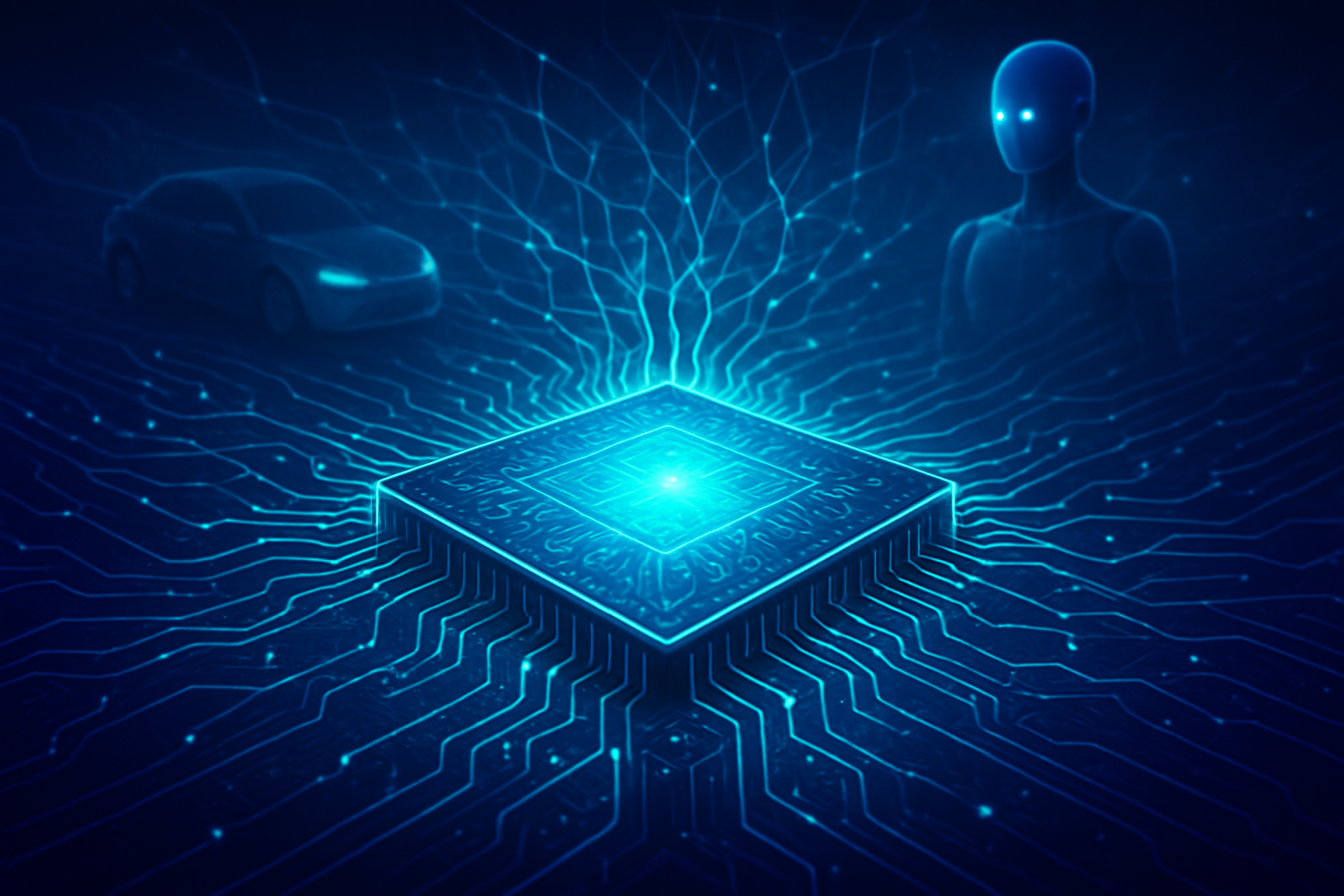
Potential applications on the horizon are vast, spanning across multiple sectors. Beyond autonomous systems and robotics, neuromorphic computing will enhance AI systems for machine learning and cognitive computing tasks, especially where energy-efficient processing is critical. It will revolutionize sensory processing for smart cameras, traffic management, and advanced voice recognition. In cybersecurity, it will enable advanced threat detection and anomaly recognition due to its rapid pattern identification capabilities. Healthcare stands to benefit significantly from real-time data processing for wearable health monitors, intelligent prosthetics, and even brain-computer interfaces (BCI). Scientific research will also be advanced through more efficient modeling and simulation in fields like neuroscience and epidemiology.
Despite this immense promise, several challenges need to be addressed. The lack of standardized benchmarks and a mature software ecosystem remains a significant hurdle. Developing algorithms that accurately mimic intricate neural processes and efficiently train spiking neural networks is complex. Hardware scalability, integration with existing systems, and manufacturing variations also pose technical challenges. Furthermore, current neuromorphic systems may not always match the accuracy of traditional computers for certain tasks, and the interdisciplinary nature of the field requires extensive collaboration across bioscience, mathematics, neuroscience, and computer science.
However, experts are overwhelmingly optimistic. The neuromorphic computing market is projected for substantial growth, with estimates suggesting it will reach USD 54.05 billion by 2035, driven by the demand for higher-performing integrated circuits and the increasing need for AI and machine learning. Many believe neuromorphic computing will revolutionize AI by enabling algorithms to run at the edge, addressing the anticipated end of Moore's Law, and significantly reducing the escalating energy demands of current AI models. The next wave of AI is expected to be a "marriage of physics and neuroscience," with neuromorphic chips leading the way to more human-like intelligence.
A New Era of Intelligence: The Road Ahead
Neuromorphic computing stands as a pivotal development in the annals of AI history, representing not merely an evolution but a fundamental re-imagination of computational architecture. Its core principle—mimicking the human brain's integrated processing and memory—offers a compelling solution to the "Von Neumann bottleneck" and the escalating energy demands of modern AI. By prioritizing energy efficiency, real-time adaptability, and on-chip learning through spiking neural networks, neuromorphic systems promise to usher in a new era of intelligent machines that are inherently more sustainable, responsive, and capable of operating autonomously in complex, dynamic environments.
The significance of this development cannot be overstated. It provides a new computational substrate that can enable the next generation of algorithmic breakthroughs, pushing the boundaries of what machines can learn and achieve. While challenges persist in terms of software ecosystems, standardization, and achieving universal accuracy, the industry is witnessing a critical inflection point as neuromorphic computing transitions from promising research to tangible commercial products.
In the coming weeks and months, the tech world will be watching for several key developments. Expect further commercialization and product rollouts from major players like Intel (NASDAQ: INTC) with its Loihi series and BrainChip (ASX: BRN) with its Akida processor, alongside innovative startups like Innatera. Increased funding and investment in neuromorphic startups will signal growing confidence in the market. Key milestones anticipated for 2026 include the establishment of standardized neuromorphic benchmarks through IEEE P2800, mass production of neuromorphic microcontrollers, and the potential approval of the first medical devices powered by this technology. The integration of neuromorphic edge AI into consumer electronics, IoT, and lifestyle devices, possibly showcased at events like CES 2026, will mark a significant step towards mainstream adoption. Continued advancements in materials, architectures, and user-friendly software development tools will be crucial for wider acceptance. Furthermore, strategic partnerships between academia and industry, alongside growing industry adoption in niche verticals like cybersecurity, event-based vision, and autonomous robotics, will underscore the technology's growing impact. The exploration by companies like Mercedes-Benz (FWB: MBG) into BrainChip's Akida for in-vehicle AI highlights the tangible interest from major industries.
Neuromorphic computing is not just a technological advancement; it's a philosophical leap towards building AI that more closely resembles biological intelligence. As we move closer to replicating the brain's incredible efficiency and adaptability, the long-term impact on healthcare, autonomous systems, edge computing, and even our understanding of intelligence itself will be profound. The journey from silicon to synthetic consciousness is long, but neuromorphic architectures are undoubtedly paving a fascinating and critical path forward.
This content is intended for informational purposes only and represents analysis of current AI developments.
TokenRing AI delivers enterprise-grade solutions for multi-agent AI workflow orchestration, AI-powered development tools, and seamless remote collaboration platforms.
For more information, visit https://www.tokenring.ai/.