As the world grapples with the insatiable energy demands of the generative AI boom and the continuing transition to electric mobility, two semiconductor titans have joined forces to redefine power efficiency. onsemi (Nasdaq: ON) and GlobalFoundries (Nasdaq: GFS) have officially launched a strategic collaboration to develop and manufacture advanced 200mm Gallium Nitride (GaN)-on-silicon power devices. With customer sampling scheduled to begin in the first half of 2026, this partnership marks a pivotal shift in the semiconductor landscape, moving GaN technology from a niche high-performance material to a mainstream industrial pillar capable of sustaining the next decade of technological expansion.
The announcement comes at a critical juncture for the industry. While traditional silicon has long been the backbone of power electronics, its physical limitations are becoming a bottleneck for high-density environments like AI data centers. By leveraging the superior bandgap properties of Gallium Nitride and scaling production to 200mm wafers—a significant upgrade from the industry-standard 150mm—Onsemi and GlobalFoundries are positioning themselves to deliver the power density required to run the massive GPU clusters and high-speed charging systems of tomorrow.
Scaling Power: The Technical Edge of 200mm GaN-on-Silicon
At the heart of this partnership is GlobalFoundries’ state-of-the-art 200mm eMode (enhancement-mode) GaN-on-silicon process. Traditionally, GaN production has been hampered by smaller wafer sizes, which increased costs and limited volume. The move to 200mm wafers allows for significantly higher yields and better economies of scale, making GaN a cost-competitive alternative to silicon in high-voltage applications. The initial rollout will focus on 650V power devices, designed to handle the rigorous electrical loads of modern infrastructure while maintaining a footprint much smaller than current silicon-based solutions.
The collaboration goes beyond mere manufacturing; it integrates Onsemi’s deep expertise in power system design, including silicon drivers, controllers, and thermally enhanced packaging. These new devices will feature "integrated functionality," combining the GaN FET (Field-Effect Transistor) with protection circuitry and drivers in a single package. This integration is crucial for reducing electromagnetic interference (EMI) and simplifying the design of complex power supplies. Furthermore, the technology supports bidirectional topologies, allowing a single component to handle power flow in both directions—a game-changer for grid-to-vehicle charging and energy storage systems.
Industry experts have noted that this approach differs fundamentally from previous GaN implementations, which were often discrete components that required complex external circuitry. By providing a "system-in-package" solution, Onsemi and GlobalFoundries are lowering the barrier to entry for engineers. Initial reactions from the hardware research community highlight that the 200mm scale effectively signals the "industrialization" of GaN, moving it away from boutique applications and into the high-volume production lines that power the global economy.
Strategic Advantage: Securing the AI and EV Supply Chain
The strategic implications for onsemi (Nasdaq: ON) and GlobalFoundries (Nasdaq: GFS) are profound. For GlobalFoundries, this partnership utilizes its U.S.-based manufacturing capacity to provide a resilient, domestic supply chain for critical power electronics—an increasingly important factor in a geopolitically sensitive semiconductor market. For Onsemi, it cements their role as a total solution provider for power management, moving them closer to becoming the preferred partner for hyperscalers and automotive OEMs (Original Equipment Manufacturers).
For the broader tech ecosystem, the primary beneficiaries are the "Magnificent Seven" and other AI labs currently struggling with data center power density. As AI racks move from 20kW to over 100kW, the efficiency gains of GaN—which can operate at much higher frequencies than silicon—allow for smaller, cooler power blocks. This frees up physical space within the rack for more H100 or B200 GPUs, effectively increasing the "compute per square foot" metric that governs the profitability of modern data centers.
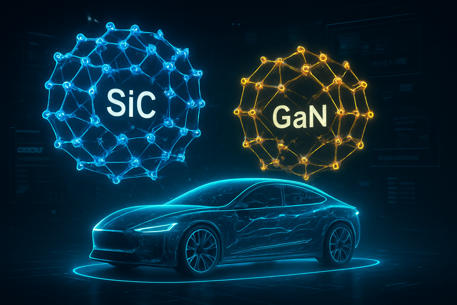
In the automotive sector, this partnership challenges the dominance of Silicon Carbide (SiC). While SiC remains the king of the main traction inverter, GaN is rapidly becoming the preferred choice for On-Board Chargers (OBC) and DC-DC converters. The ability to charge faster and reduce the weight of power conversion systems directly translates to longer range and lower costs for electric vehicle manufacturers. By providing a scalable, high-volume GaN solution, the Onsemi-GF partnership creates a significant competitive hurdle for smaller GaN startups that lack the manufacturing muscle to meet the demands of global auto fleets.
The Global Impact: Solving the AI Energy Crisis
The significance of this partnership extends far beyond corporate balance sheets; it addresses a fundamental challenge of the current AI era: the energy crisis. Current AI workloads are consuming power at an exponential rate, leading to concerns about the sustainability of the digital revolution. GaN technology is estimated to be up to 40% more efficient than traditional silicon in power conversion. If applied across the global network of AI data centers, the resulting energy savings could represent terawatt-hours of electricity, aligning technological progress with global carbon reduction goals.
This development also reflects a broader trend toward "power-conscious computing." In the past, hardware performance was measured primarily by clock speeds and core counts. Today, the metric of success is shifting toward performance-per-watt. The transition to 200mm GaN-on-silicon is perhaps the most significant milestone in power electronics since the introduction of the MOSFET, as it marks the moment high-efficiency wide-bandgap semiconductors become a mass-market reality.
However, the transition is not without hurdles. The industry must still address the long-term reliability of GaN under extreme thermal stress compared to the decades of data available for silicon. Comparison to previous milestones, like the transition from vacuum tubes to transistors, might seem hyperbolic, but in the context of power density, the move to integrated GaN-on-silicon represents a similar generational leap in how we manage and deploy electrical energy.
The Road Ahead: Sampling and Mass Adoption
Looking forward, the immediate focus is the H1 2026 sampling window. During this phase, major cloud providers and automotive Tier-1 suppliers will begin integrating these 200mm GaN devices into their prototype systems. If successful, we can expect to see the first GaN-powered AI server racks hitting the market by late 2026. In the automotive sector, the impact will likely be felt in the 2027 and 2028 model-year vehicles, where integrated GaN components will help drive down the MSRP of EVs by reducing the cost and complexity of the internal power architecture.
In the long term, experts predict that this partnership will pave the way for GaN to enter even more sensitive markets, such as aerospace and defense, where the weight savings of GaN are highly valued. The ultimate goal is a world where power conversion is nearly lossless and virtually invisible, integrated directly into the silicon of the processors themselves. While there are still challenges regarding the cost of raw materials and manufacturing yields at the 200mm scale, the combined weight of Onsemi and GlobalFoundries suggests these hurdles are surmountable.
Final Thoughts: A New Power Standard
The Onsemi and GlobalFoundries partnership represents a defining moment for the semiconductor industry. By focusing on 200mm GaN-on-silicon, these companies are not just launching a product; they are establishing a new standard for power efficiency that will support the most demanding technologies of the 21st century. The move targets the two most critical drivers of the modern economy: the expansion of artificial intelligence and the electrification of transport.
As we move into the first half of 2026, the tech world will be watching the sampling results closely. The success of this collaboration will likely dictate the pace of AI infrastructure expansion and the feasibility of mass-market EV adoption. In the history of AI, we may look back at 2026 as the year the "power problem" finally met its match, enabling the next great wave of digital and physical innovation.
This content is intended for informational purposes only and represents analysis of current AI and semiconductor developments.
TokenRing AI delivers enterprise-grade solutions for multi-agent AI workflow orchestration, AI-powered development tools, and seamless remote collaboration platforms.
For more information, visit https://www.tokenring.ai/.