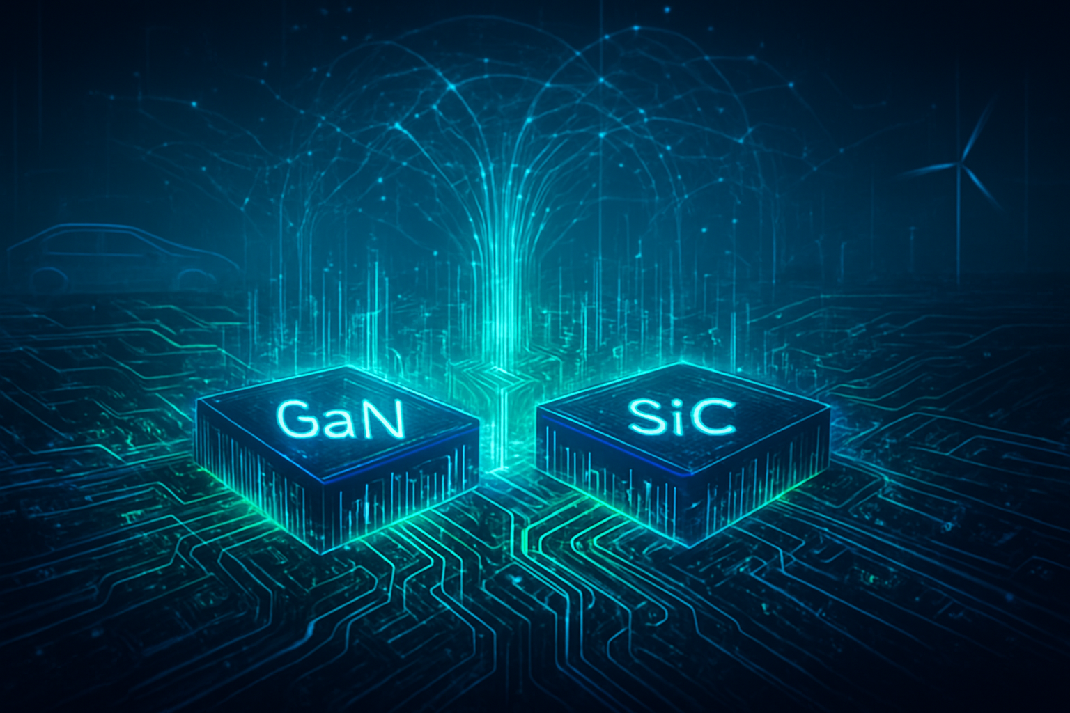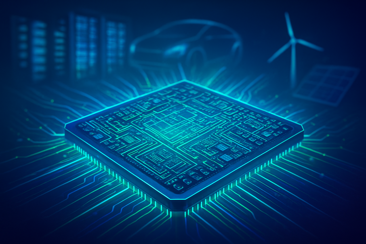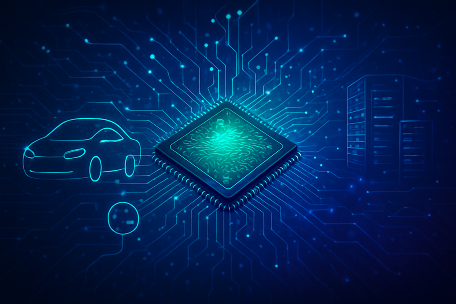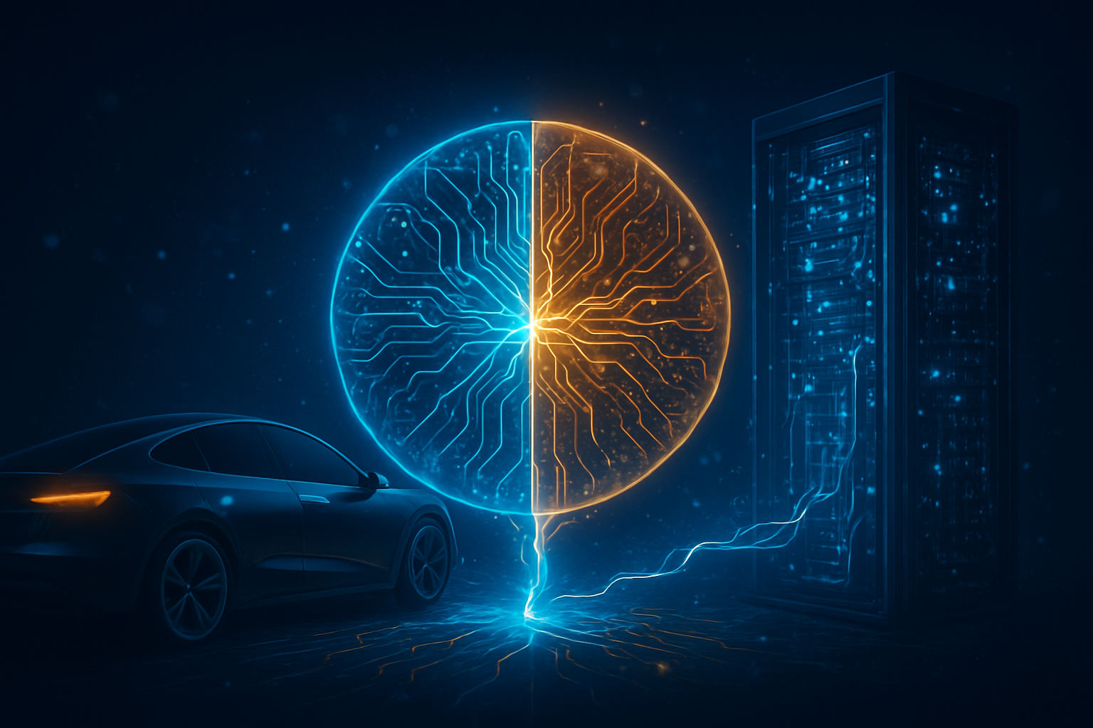
The era of traditional silicon dominance in high-power electronics has officially reached its twilight. As of late 2025, the global technology landscape is undergoing a foundational shift toward wide-bandgap (WBG) materials—specifically Silicon Carbide (SiC) and Gallium Nitride (GaN). These materials, once relegated to niche industrial applications, have become the indispensable backbone of two of the most critical sectors of the modern economy: the rapid expansion of artificial intelligence data centers and the global transition to high-performance electric vehicles (EVs).
This transition is driven by a simple but brutal reality: the "Energy Wall." With the latest AI chips drawing unprecedented amounts of power and EVs demanding faster charging times to achieve mass-market parity with internal combustion engines, traditional silicon can no longer keep up. SiC and GaN offer the physical properties necessary to handle higher voltages, faster switching frequencies, and extreme temperatures, all while significantly reducing energy loss. This shift is not just an incremental improvement; it is a complete re-architecting of how the world manages and consumes electrical power.
The Technical Shift: Breaking the Energy Wall
The technical superiority of SiC and GaN lies in their "wide bandgap," a property that allows these semiconductors to operate at much higher voltages and temperatures than standard silicon. In the world of AI, this has become a necessity. As NVIDIA (NASDAQ: NVDA) rolls out its Blackwell Ultra and the highly anticipated Vera Rubin GPU architectures, power consumption per rack has skyrocketed. A single Rubin-class GPU package is estimated to draw between 1.8kW and 2.0kW. To support this, data center power supply units (PSUs) have had to evolve. Using GaN, companies like Navitas Semiconductor (NASDAQ: NVTS) and Infineon Technologies (OTC: IFNNY) have developed 12kW PSUs that fit into the same physical footprint as older 3kW silicon models, effectively quadrupling power density.
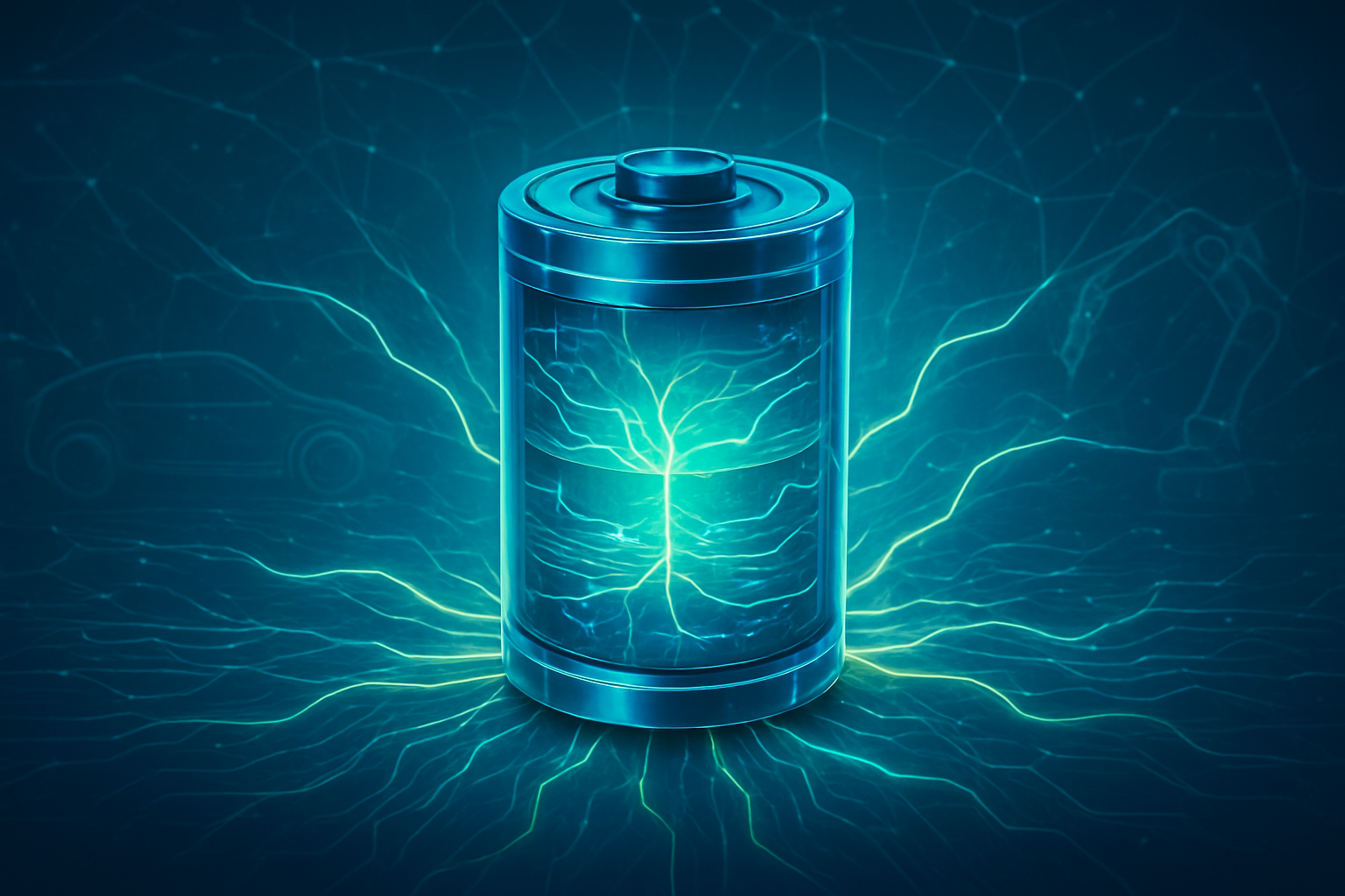
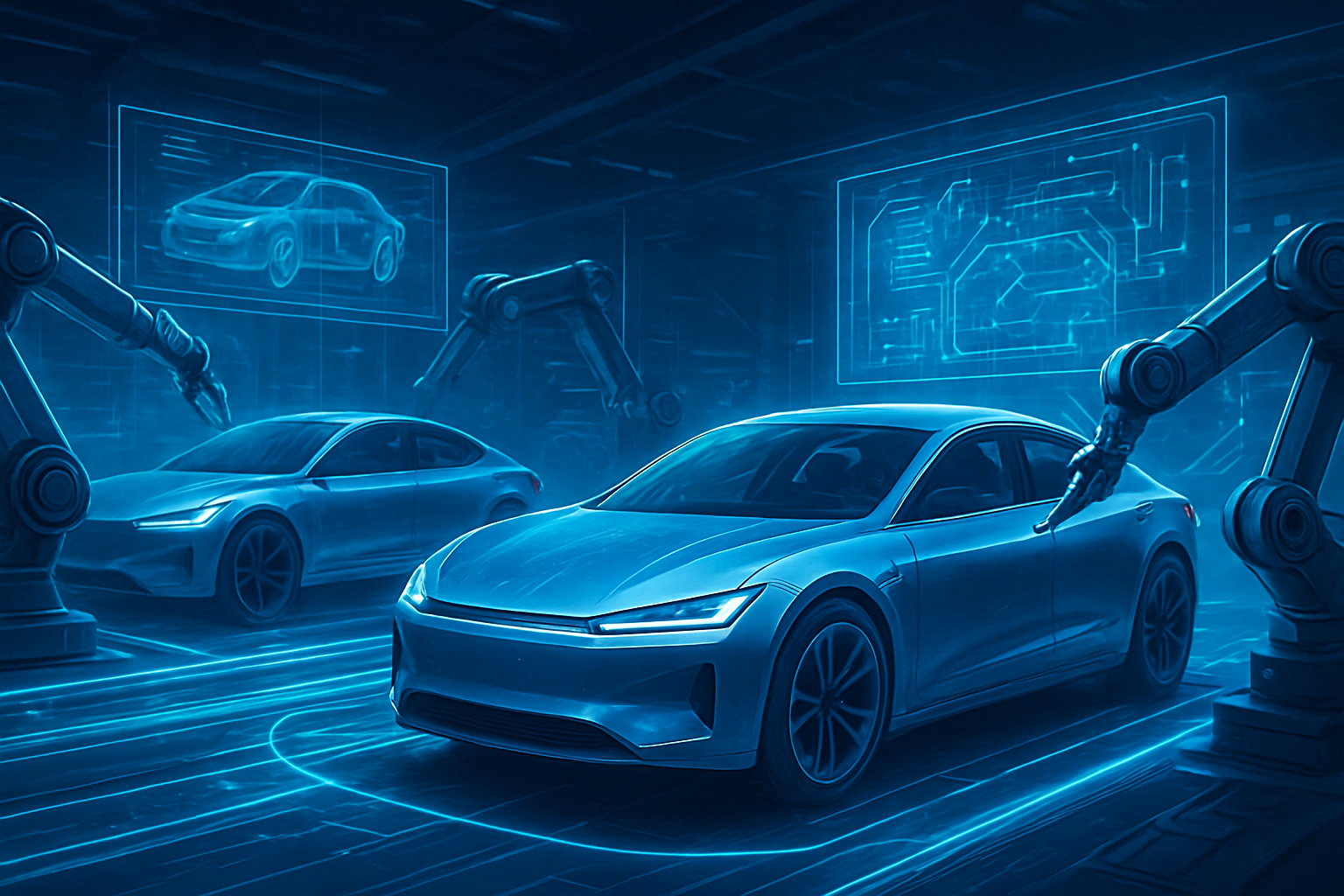
In the EV sector, the transition to 800-volt architectures has become the industry standard for 2025. Silicon Carbide is the hero of this transition, enabling traction inverters that are 3x smaller and significantly more efficient than their silicon predecessors. This efficiency directly translates to increased range and the ability to support "Mega-Fast" charging. With SiC-based systems, new models from Tesla (NASDAQ: TSLA) and BYD (OTC: BYDDF) are now capable of adding 400km of range in as little as five minutes, effectively eliminating "range anxiety" for the next generation of drivers.
The manufacturing process has also hit a major milestone in late 2025: the maturation of 200mm (8-inch) SiC wafer production. For years, the industry struggled to move beyond 150mm wafers due to the difficulty of growing high-quality SiC crystals. The successful shift to 200mm by leaders like STMicroelectronics (NYSE: STM) and onsemi (NASDAQ: ON) has increased chip yields by nearly 80% per wafer, finally bringing the cost of these advanced materials down toward parity with high-end silicon.
Market Dynamics: Winners, Losers, and Strategic Shifts
The market for power semiconductors has seen dramatic volatility and consolidation throughout 2025. The most shocking development was the mid-year Chapter 11 bankruptcy filing of Wolfspeed (NYSE: WOLF), formerly the standard-bearer for SiC technology. Despite massive government subsidies, the company struggled with the astronomical capital expenditures required for its Mohawk Valley fab and was ultimately undercut by a surge of low-cost SiC substrates from Chinese competitors like SICC and Sanan Optoelectronics. This has signaled a shift in the industry toward "vertical integration" and diversified portfolios.
Conversely, STMicroelectronics has solidified its position as the market leader. By securing deep partnerships with both Western EV giants and Chinese manufacturers, STM has created a resilient supply chain that spans continents. Meanwhile, Infineon Technologies has taken the lead in the "GaN-on-Silicon" race, successfully commercializing 300mm (12-inch) GaN wafers. This breakthrough has allowed them to dominate the AI data center market, providing the high-frequency switches needed for the "last inch" of power delivery—stepping down voltage directly on the GPU substrate to minimize transmission losses.
The competitive implications are clear: companies that failed to transition to 200mm SiC or 300mm GaN fast enough are being marginalized. The barrier to entry has moved from "can you make it?" to "can you make it at scale and at a competitive price?" This has led to a flurry of strategic alliances, such as the one between onsemi and major AI server integrators, to ensure a steady supply of their new "Vertical GaN" (vGaN) chips, which can handle the 1200V+ requirements of industrial AI fabs.
Wider Significance: Efficiency as a Climate Imperative
Beyond the balance sheets of tech giants, the rise of SiC and GaN represents a significant win for global sustainability. AI data centers are on track to consume nearly 10% of global electricity by 2030 if efficiency gains are not realized. The adoption of GaN-based power supplies, which operate at up to 98% efficiency (meeting the 80 PLUS Titanium standard), is estimated to save billions of kilowatt-hours annually. This "negawatt" production—energy saved rather than generated—is becoming a central pillar of corporate ESG strategies.
However, this transition also brings concerns regarding supply chain sovereignty. With China currently dominating the production of raw SiC substrates and aggressively driving down prices, Western nations are racing to build "circular" supply chains. The environmental impact of manufacturing these materials is also under scrutiny; while they save energy during their lifecycle, the initial production of SiC and GaN is more energy-intensive than traditional silicon.
Comparatively, this milestone is being viewed by industry experts as the "LED moment" for power electronics. Just as LEDs replaced incandescent bulbs by offering ten times the efficiency and longevity, WBG materials are doing the same for the power grid. It is a fundamental decoupling of economic growth (in AI and mobility) from linear increases in energy consumption.
Future Outlook: Vertical GaN and the Path to 2030
Looking toward 2026 and beyond, the next frontier is "Vertical GaN." While current GaN technology is primarily lateral and limited to lower voltages, vGaN promises to handle 1200V and above, potentially merging the benefits of SiC (high voltage) and GaN (high frequency) into a single material. This would allow for even smaller, more integrated power systems that could eventually find their way into consumer electronics, making "brick" power adapters a thing of the past.
Experts also predict the rise of "Power-on-Package" (PoP) for AI. In this scenario, the entire power conversion stage is integrated directly into the GPU or AI accelerator package using GaN micro-chips. This would eliminate the need for bulky voltage regulators on the motherboard, allowing for even denser server configurations. The challenge remains the thermal management of such highly concentrated power, which will likely drive further innovation in liquid and phase-change cooling.
A New Era for the Silicon World
The rise of Silicon Carbide and Gallium Nitride marks the end of the "Silicon-only" era and the beginning of a more efficient, high-density future. As of December 2025, the results are evident: EVs charge faster and travel further, while AI data centers are managing to scale their compute capabilities without collapsing the power grid. The downfall of early pioneers like Wolfspeed serves as a cautionary tale of the risks inherent in such a rapid technological pivot, but the success of STMicro and Infineon proves that the rewards are equally massive.
In the coming months, the industry will be watching for the first deployments of NVIDIA’s Rubin systems and the impact they have on the power supply chain. Additionally, the continued expansion of 200mm SiC manufacturing will be the key metric for determining how quickly these advanced materials can move from luxury EVs to the mass market. For now, the "Power Wall" has been breached, and the future of technology is looking brighter—and significantly more efficient.
This content is intended for informational purposes only and represents analysis of current AI developments.
TokenRing AI delivers enterprise-grade solutions for multi-agent AI workflow orchestration, AI-powered development tools, and seamless remote collaboration platforms.
For more information, visit https://www.tokenring.ai/.