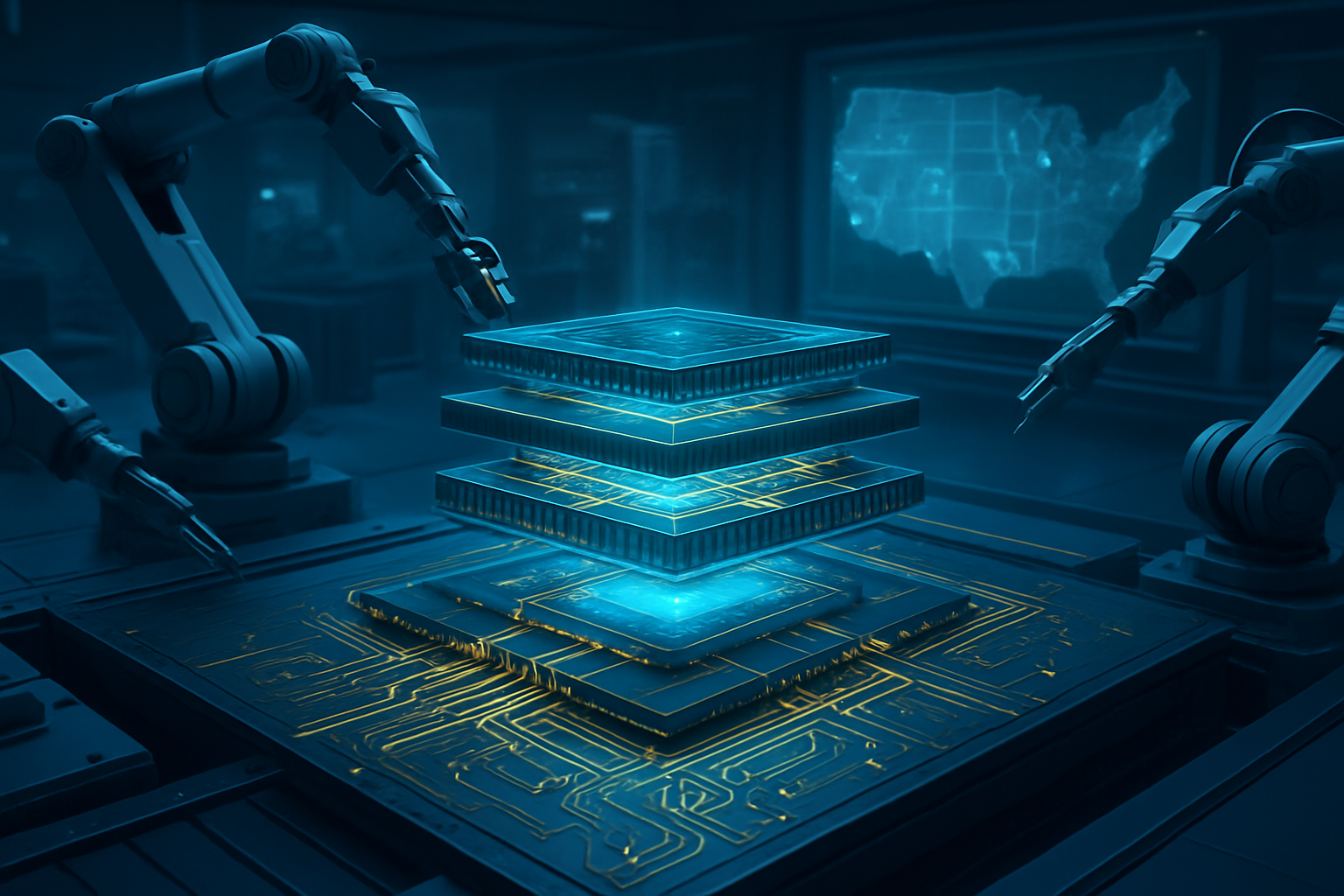
At the prestigious NEPCON Japan 2026 exhibition in Tokyo, Intel (NASDAQ: INTC) has fundamentally altered the roadmap for high-performance computing by unveiling its first "thick-core" glass substrate technology. The demonstration of a 10-2-10-thick glass core substrate marks a historic transition away from traditional organic materials, promising to unlock the next level of scalability for massive AI accelerators and data center processors. By integrating this glass architecture with its proprietary Embedded Multi-die Interconnect Bridge (EMIB) packaging, Intel has showcased a path to chips that are twice the size of current limits, effectively bypassing the physical constraints that have plagued the industry for years.
The significance of this announcement cannot be overstated. As AI models grow in complexity, the chips required to train them have reached a "reticle limit"—a size barrier beyond which traditional manufacturing cannot go without compromising structural integrity. Intel’s move to glass substrates addresses the "warpage wall," a phenomenon where organic materials flex and distort under the extreme heat and pressure of advanced chip manufacturing. This breakthrough positions Intel Foundry as a frontrunner in the "system-in-package" era, offering a solution that its competitors are still racing to stabilize.
Engineering the 10-2-10 Architecture: A Technical Leap
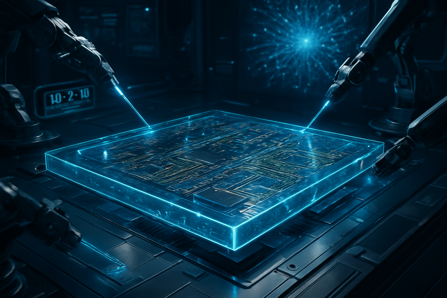
The centerpiece of Intel’s showcase is the 10-2-10 glass substrate, a naming convention that refers to its sophisticated vertical architecture. The substrate features a dual-layer glass core, with each layer measuring approximately 800 micrometers, creating a robust 1.6 mm "thick-core" foundation. This central glass pillar is flanked by ten high-density redistribution layers (RDL) on the top and another ten on the bottom. These layers enable ultra-fine-pitch routing down to 45 μm, allowing for thousands of microscopic connections between the silicon die and the substrate with unprecedented signal clarity.
Unlike the industry-standard Ajinomoto Build-up Film (ABF) organic substrates, glass possesses a Coefficient of Thermal Expansion (CTE) that nearly matches silicon. This property is the key to solving the "warpage wall." Intel reported that across its massive 78 × 77 mm package, warpage was held to less than 20 μm—a staggering improvement over the 50 μm or more seen in organic cores. By maintaining near-perfect flatness during the high-heat bonding process, Intel can ensure the reliability of microscopic solder bumps that would otherwise crack or fail in a traditional organic package.
Furthermore, Intel has successfully integrated its EMIB technology directly into the glass structure. The NEPCON demonstration featured two silicon bridges embedded within the glass, facilitating lightning-fast communication between logic chiplets and High-Bandwidth Memory (HBM). This integration allows for a total silicon area of roughly 1,716 mm², which is approximately twice the standard reticle size of current lithography tools. This "double-reticle" capability means AI chip designers can effectively double the compute density of a single package without the yield losses associated with monolithic mammoth chips.
Shifting the Competitive Landscape: NVIDIA and the Foundry Wars
Intel’s early lead in glass substrates has immediate implications for the broader semiconductor market. For years, NVIDIA (NASDAQ: NVDA) and AMD (NASDAQ: AMD) have been heavily reliant on the Chip-on-Wafer-on-Substrate (CoWoS) packaging capacity of TSMC (NYSE: TSM). However, as of early 2026, CoWoS remains constrained by the inherent limitations of organic substrates for ultra-large chips. Intel’s "Foundry-first" strategy at NEPCON Japan signals that it is ready to offer a "waitlist-free" alternative for companies hitting the physical limits of current packaging.
Industry analysts at the event noted that major players like Apple (NASDAQ: AAPL) and NVIDIA are already in preliminary discussions with Intel to secure glass substrate capacity for their 2027 and 2028 product cycles. By proving that it can move glass substrates into high-volume manufacturing (HVM) at its Chandler, Arizona facility, Intel is creating a significant strategic advantage over Samsung (KRX: 005930), which is currently leveraging its "Triple Alliance" of display and electro-mechanics divisions to target a late 2026 mass production date.
The disruption extends to the very structure of AI hardware. While TSMC is developing its own glass-based CoPoS (Chip-on-Panel-on-Substrate) technology, it is not expected to reach full panel-level production until 2027. This gives Intel a nearly 18-month window to establish its glass-core ecosystem as the gold standard for the most demanding AI workloads. For startups and smaller AI labs, Intel’s move could democratize access to extreme-scale computing power, as the higher yields of chiplet-based glass packaging could eventually drive down the astronomical costs of flagship AI accelerators.
Beyond Moore’s Law: The Wider Significance for Artificial Intelligence
The transition to glass substrates is more than a material change; it is a fundamental shift in how the industry approaches the limits of Moore’s Law. As traditional transistor scaling slows down, "More than Moore" scaling through advanced packaging has become the primary driver of performance gains. Glass provides the thermal stability and interconnect density required to power the next generation of 1,000-watt-plus AI processors, which would be physically impossible to package reliably using organic materials.
However, the move to glass is not without its concerns. The brittle nature of glass has historically led to "SeWaRe" (Selective Wave Refraction) micro-cracking during the drilling and dicing processes. Intel’s announcement that it has solved these manufacturing hurdles is a major milestone, but the long-term durability of glass substrates in high-vibration data center environments remains a topic of intense study. Critics also point out that the specialized manufacturing equipment required for glass handling represents a massive capital expenditure, potentially consolidating power among only the wealthiest foundries.
Despite these challenges, the broader AI landscape stands to benefit immensely. The ability to support twice the reticle size allows for the creation of "super-chips" that can hold larger on-die LLM weights, reducing the need for off-chip communication and drastically lowering the energy required for inference and training. In an era where power consumption is the ultimate bottleneck for AI expansion, the thermal efficiency of glass could be the industry’s most important breakthrough since the invention of the FinFET.
The Horizon: What’s Next for Glass Substrates
Looking ahead, the near-term focus will be on Intel’s first commercial implementation of this technology, expected in the "Clearwater Forest" Xeon processors. Following this, the industry anticipates a rapid expansion of the glass ecosystem. By 2027, experts predict that the 10-2-10 architecture will evolve into even more complex stacks, potentially reaching 15-2-15 configurations as the industry pushes toward trillion-transistor packages.
The next major challenge will be the standardization of glass panel sizes. Currently, different foundries are experimenting with various dimensions, but a move toward a universal panel standard—similar to the 300mm wafer standard—will be necessary to drive down costs through economies of scale. Additionally, the integration of optical interconnects directly into the glass substrate is on the horizon, which could eliminate electrical resistance entirely for chip-to-chip communication.
A New Era for Semiconductor Manufacturing
Intel’s unveiling at NEPCON Japan 2026 marks the end of the organic substrate era for high-end computing. By successfully navigating the technical minefield of glass manufacturing and integrating it with EMIB, Intel has provided a tangible solution to the "warpage wall" and the reticle limit. This development is not just an incremental improvement; it is a foundational change that will dictate the design of AI hardware for the next decade.
As we move into the middle of 2026, the industry will be watching Intel's production yields closely. If the 10-2-10 thick-core substrate performs as promised in real-world data center environments, it will solidify Intel’s position at the heart of the AI revolution. For now, the message from Tokyo is clear: the future of AI is transparent, rigid, and made of glass.
This content is intended for informational purposes only and represents analysis of current AI developments.
TokenRing AI delivers enterprise-grade solutions for multi-agent AI workflow orchestration, AI-powered development tools, and seamless remote collaboration platforms.
For more information, visit https://www.tokenring.ai/.