Tag: EUV

  • The Silicon Fortress: China’s Multi-Billion Dollar Consolidation and the Secret ‘EUV Manhattan Project’ Reshaping Global AI

    The Silicon Fortress: China’s Multi-Billion Dollar Consolidation and the Secret ‘EUV Manhattan Project’ Reshaping Global AI

    As of January 7, 2026, the global semiconductor landscape has reached a definitive tipping point. Beijing has officially transitioned from a defensive posture against Western export controls to an aggressive, "whole-of-nation" consolidation of its domestic chip industry. In a series of massive strategic maneuvers, China has funneled tens of billions of dollars into its primary national champions, effectively merging fragmented state-backed entities into a cohesive "Silicon Fortress." This consolidation is not merely a corporate restructuring; it is the structural foundation for China’s "EUV Manhattan Project," a secretive, high-stakes endeavor to achieve total independence from Western lithography technology.

    The immediate significance of these developments cannot be overstated. By unifying the balance sheets and R&D pipelines of its largest foundries, China is attempting to bypass the "chokepoints" established by the U.S. and its allies. The recent announcement of a functional indigenous Extreme Ultraviolet (EUV) lithography prototype—a feat many Western experts predicted would take a decade—suggests that the massive capital injections from the "Big Fund Phase 3" are yielding results far faster than anticipated. This shift marks the beginning of a sovereign AI compute stack, where every component, from the silicon to the software, is produced within Chinese borders.

    The Technical Vanguard: Consolidation and the LDP Breakthrough

    At the heart of this consolidation are two of China’s most critical players: Semiconductor Manufacturing International Corporation (SHA: 688981 / HKG: 0981), known as SMIC, and Hua Hong Semiconductor (SHA: 688347 / HKG: 1347). In late 2024 and throughout 2025, SMIC executed a 40.6 billion yuan ($5.8 billion) deal to consolidate its "SMIC North" subsidiary, streamlining the governance of its most advanced 28nm and 7nm production lines. Simultaneously, Hua Hong completed a $1.2 billion acquisition of Shanghai Huali Microelectronics, unifying the group’s specialty process technologies. These deals have eliminated internal competition for talent and resources, allowing for a concentrated push toward 5nm and 3nm nodes.

    Technically, the most staggering advancement is the reported success of the "EUV Manhattan Project." While ASML (NASDAQ: ASML) has long held a monopoly on EUV technology using Laser-Produced Plasma (LPP), Chinese researchers, coordinated by Huawei and state institutes, have reportedly operationalized a prototype using Laser-Induced Discharge Plasma (LDP). This alternative method is touted as more energy-efficient and potentially easier to scale than the complex LPP systems. As of early 2026, the prototype has successfully generated 13.5nm EUV light at power levels nearing 100W, a critical threshold for commercial viability.

    This technical pivot differs from previous Chinese efforts which relied on "brute-force" multi-patterning using older Deep Ultraviolet (DUV) machines. While multi-patterning allowed SMIC to produce 7nm chips for Huawei’s smartphones, the yields were historically low and costs were prohibitively high. The move to indigenous EUV, combined with advanced 2.5D and 3D packaging from firms like JCET Group (SHA: 600584), allows China to move toward "chiplet" architectures. This enables the assembly of high-performance AI accelerators by stitching together multiple smaller dies, effectively matching the performance of cutting-edge Western chips without needing a single, perfect 3nm die.

    Market Repercussions: The Rise of the Sovereign AI Stack

    The consolidation of SMIC and Hua Hong creates a formidable competitive environment for global tech giants. For years, NVIDIA (NASDAQ: NVDA) and other Western firms have navigated a complex web of sanctions to sell "downgraded" chips to the Chinese market. However, with the emergence of a consolidated domestic supply chain, Chinese AI labs are increasingly turning to the Huawei Ascend 950 series, manufactured on SMIC’s refined 7nm and 5nm lines. This development threatens to permanently displace Western silicon in one of the world’s largest AI markets, as Chinese firms prioritize "sovereign compute" over international compatibility.

    Major AI labs and domestic startups in China, such as those behind the Qwen and DeepSeek models, are the primary beneficiaries of this consolidation. By having guaranteed access to domestic foundries that are no longer subject to foreign license revocations, these companies can scale their training clusters with a level of certainty that was missing in 2023 and 2024. Furthermore, the strategic focus of the "Big Fund Phase 3"—which launched with $47.5 billion in capital—has shifted toward High-Bandwidth Memory (HBM). ChangXin Memory (CXMT) is reportedly nearing mass production of HBM3, the vital "fuel" for AI processors, further insulating the domestic market from global supply shocks.

    For Western companies, the disruption is twofold. First, the loss of Chinese revenue impacts the R&D budgets of firms like Intel (NASDAQ: INTC) and AMD (NASDAQ: AMD). Second, the "brute-force" innovation occurring in China is driving down the cost of mature-node chips (28nm and above), which are essential for automotive and IoT AI applications. As Hua Hong and SMIC flood the market with these consolidated, state-subsidized products, global competitors may find it impossible to compete on price, leading to a potential "hollowing out" of the mid-tier semiconductor market outside of the U.S. and Europe.

    A New Era of Geopolitical Computing

    The broader significance of China’s semiconductor consolidation lies in the formalization of the "Silicon Curtain." We are no longer looking at a globalized supply chain with minor friction; we are witnessing the birth of two entirely separate, mutually exclusive tech ecosystems. This trend mirrors the Cold War era's space race, but with the "EUV Manhattan Project" serving as the modern-day equivalent of the Apollo program. The goal is not just to make chips, but to ensure that the fundamental infrastructure of the 21st-century economy—Artificial Intelligence—is not dependent on a geopolitical rival.

    This development also highlights a significant shift in AI milestones. While the 2010s were defined by breakthroughs in deep learning and transformers, the mid-2020s are being defined by the "hardware-software co-design" at a national level. China’s ability to improve 5nm yields to a commercially viable 30-40% using domestic tools is a milestone that many industry analysts thought impossible under current sanctions. It proves that "patient capital" and state-mandated consolidation can, in some cases, overcome the efficiencies of a free-market global supply chain when the goal is national survival.

    However, this path is not without its concerns. The extreme secrecy surrounding the EUV project and the aggressive recruitment of foreign talent have heightened international tensions. There are also questions regarding the long-term sustainability of this "brute-force" model. While the government can subsidize yields and capital expenditures indefinitely, the lack of exposure to the global competitive market could eventually lead to stagnation in innovation once the immediate "catch-up" phase is complete. Comparisons to the Soviet Union's microelectronics efforts in the 1970s are frequent, though China’s vastly superior manufacturing base makes this a much more potent threat to Western hegemony.

    The Road to 2027: What Lies Ahead

    In the near term, the industry expects SMIC to double its 7nm capacity by the end of 2026, providing the silicon necessary for a massive expansion of China’s domestic cloud AI infrastructure. The "EUV Manhattan Project" is expected to move from its current prototype phase to pilot testing of "EUV-refined" 5nm chips at specialized facilities in Shenzhen and Dongguan. Experts predict that while full-scale commercial production using indigenous EUV is still several years away (likely 2028-2030), the psychological and strategic impact of a working prototype will accelerate domestic investment even further.

    The next major challenge for Beijing will be the "materials chokepoint." While they have consolidated the foundries and are nearing a lithography breakthrough, China still remains vulnerable in the areas of high-end photoresists and ultra-pure chemicals. We expect the next phase of the Big Fund to focus almost exclusively on these "upstream" materials. If China can achieve the same level of consolidation in its chemical and materials science sectors as it has in its foundries, the goal of 100% AI chip self-sufficiency by 2027—once dismissed as propaganda—could become a reality.

    Closing the Loop on Silicon Sovereignty

    The strategic consolidation of China’s semiconductor industry under SMIC and Hua Hong, fueled by the massive capital of Big Fund Phase 3, represents a tectonic shift in the global order. By January 2026, the "EUV Manhattan Project" has moved from a theoretical ambition to a tangible prototype, signaling that the era of Western technological containment may be nearing its limits. The creation of a sovereign AI stack is no longer a distant dream for Beijing; it is a functioning reality that is already beginning to power the next generation of Chinese AI models.

    This development will likely be remembered as a pivotal moment in AI history—the point where the "compute divide" became permanent. As China scales its domestic production and moves toward 5nm and 3nm nodes through innovative packaging and indigenous lithography, the global tech industry must prepare for a world of bifurcated standards and competing silicon ecosystems. In the coming months, the key metrics to watch will be the yield rates of SMIC’s 5nm lines and the progress of CXMT’s HBM3 mass production. These will be the true indicators of whether China’s "Silicon Fortress" can truly stand the test of time.


    This content is intended for informational purposes only and represents analysis of current AI developments.

    TokenRing AI delivers enterprise-grade solutions for multi-agent AI workflow orchestration, AI-powered development tools, and seamless remote collaboration platforms.
    For more information, visit https://www.tokenring.ai/.

  • High-NA EUV Era Begins: Intel Deploys First ASML Tool as China Signals EUV Prototype Breakthrough

    High-NA EUV Era Begins: Intel Deploys First ASML Tool as China Signals EUV Prototype Breakthrough

    The global semiconductor landscape reached a historic inflection point in late 2025 as Intel Corporation (NASDAQ: INTC) announced the successful installation and acceptance testing of the industry's first commercial High-Numerical Aperture (High-NA) Extreme Ultraviolet (EUV) lithography tool. The machine, a $350 million ASML (NASDAQ: ASML) Twinscan EXE:5200B, represents the most advanced piece of manufacturing equipment ever created, signaling the start of the "Angstrom Era" in chip production. By securing the first of these massive systems, Intel aims to leapfrog its rivals and reclaim the crown of transistor density and power efficiency.

    However, the Western technological lead is facing an unprecedented challenge from the East. Simultaneously, reports have emerged from Shenzhen, China, indicating that a domestic research consortium has validated a working EUV prototype. This breakthrough, part of a state-sponsored "Manhattan Project" for semiconductors, suggests that China is making rapid progress in bypassing US-led export bans. While the Chinese prototype is not yet ready for high-volume manufacturing, its existence marks a significant milestone in Beijing’s quest for technological sovereignty, with a stated goal of producing domestic EUV-based processors by 2028.

    The Technical Frontier: 1.4nm and the High-NA Advantage

    The ASML Twinscan EXE:5200B is a marvel of engineering, standing nearly two stories tall and requiring multiple Boeing 747s for transport. The defining feature of this tool is its Numerical Aperture (NA), which has been increased from the 0.33 of standard EUV machines to 0.55. This jump in NA allows for an 8nm resolution, a significant improvement over the 13.5nm limit of previous generations. For Intel, this means the ability to print features for its upcoming 14A (1.4nm) node using "single-patterning." Previously, achieving such small dimensions required "multi-patterning," a process where a single layer is printed multiple times, which increases the risk of defects and dramatically raises production costs.

    Initial reactions from the semiconductor research community have been a mix of awe and cautious optimism. Dr. Aris Silzars, a veteran industry analyst, noted that the EXE:5200B’s throughput—capable of processing 175 to 200 wafers per hour—is the "holy grail" for making the 1.4nm node economically viable. The tool also boasts an overlay accuracy of 0.7 nanometers, a precision equivalent to hitting a golf ball on the moon from Earth. Experts suggest that by adopting High-NA early, Intel is effectively "de-risking" its roadmap for the next decade, while competitors like Taiwan Semiconductor Manufacturing Company (NYSE: TSM) and Samsung Electronics (KRX: 005930) have opted for a more conservative approach, extending the life of standard EUV tools through complex multi-patterning techniques.

    In contrast, the Chinese prototype developed in Shenzhen utilizes a different technical path. While ASML uses Laser-Produced Plasma (LPP) to generate EUV light, the Chinese team, reportedly led by engineers from Huawei and various state-funded institutes, has successfully demonstrated a Laser-Induced Discharge Plasma (LDP) source. Though currently producing only 100W–150W of power—roughly half of what is needed for high-speed commercial production—it proves that China has solved the fundamental physics of EUV light generation. This "Manhattan Project" approach has involved a massive mobilization of talent, including former ASML and Nikon (OTC: NINNY) engineers, to reverse-engineer the complex reflective optics and light sources that were previously thought to be decades out of reach for domestic Chinese firms.

    Strategic Maneuvers: The Battle for Lithography Leadership

    Intel’s aggressive move to install the EXE:5200B is a clear strategic play to regain the manufacturing lead it lost over the last decade. By being the first to master High-NA, Intel (NASDAQ: INTC) provides its foundry customers with a unique value proposition: the ability to manufacture the world’s most advanced AI and mobile chips with fewer processing steps and higher yields. This development puts immense pressure on TSMC (NYSE: TSM), which has dominated the 3nm and 5nm markets. If Intel can successfully ramp up the 14A node by 2026 or 2027, it could disrupt the current foundry hierarchy and attract major clients like Apple and Nvidia that have traditionally relied on Taiwanese fabrication.

    The competitive implications extend far beyond the United States and Taiwan. China's breakthrough in Shenzhen represents a direct challenge to the efficacy of the U.S. Department of Commerce's export controls. For years, the denial of EUV tools to Chinese firms like SMIC was considered a "hard ceiling" that would prevent China from progressing beyond the 7nm or 5nm nodes. The validation of a domestic EUV prototype suggests that this ceiling is cracking. If China can scale this technology, it would not only secure its own supply chain but also potentially offer a cheaper, state-subsidized alternative to the global market, disrupting the high-margin business models of Western equipment makers.

    Furthermore, the emergence of the Chinese "Manhattan Project" has sparked a new arms race in lithography. Companies like Canon (NYSE: CAJ) are attempting to bypass EUV altogether with "nanoimprint" lithography, but the industry consensus remains that EUV is the only viable path for sub-2nm chips. Intel’s first-mover advantage with the EXE:5200B creates a "financial and technical moat" that may be too expensive for smaller players to cross, potentially consolidating the leading-edge market into a triopoly of Intel, TSMC, and Samsung.

    Geopolitical Stakes and the Future of Moore’s Law

    The simultaneous announcements from Oregon and Shenzhen highlight the intensifying "Chip War" between the U.S. and China. This is no longer just a corporate competition; it is a matter of national security and economic survival. The High-NA EUV tools are the "printing presses" of the modern era, and the nation that controls them controls the future of Artificial Intelligence, autonomous systems, and advanced weaponry. Intel's success is seen as a validation of the CHIPS Act and the U.S. strategy to reshore critical manufacturing.

    However, the broader AI landscape is also at stake. As AI models grow in complexity, the demand for more transistors per square millimeter becomes insatiable. High-NA EUV is the only technology currently capable of sustaining the pace of Moore’s Law—the observation that the number of transistors on a microchip doubles about every two years. Without the precision of the EXE:5200B, the industry would likely face a "performance wall," where the energy costs of running massive AI data centers would become unsustainable.

    The potential concerns surrounding this development are primarily geopolitical. If China succeeds in its 2028 goal of domestic EUV processors, it could render current sanctions obsolete and lead to a bifurcated global tech ecosystem. We are witnessing the end of a globalized semiconductor supply chain and the birth of two distinct, competing stacks: one led by the U.S. and ASML, and another led by China’s centralized "whole-of-nation" effort. This fragmentation could lead to higher costs for consumers and a slower pace of global innovation as research is increasingly siloed behind national borders.

    The Road to 2028: What Lies Ahead

    Looking forward, the next 24 to 36 months will be critical for both Intel and the Chinese consortium. For Intel (NASDAQ: INTC), the challenge is transitioning from "installation" to "yield." It is one thing to have a $350 million machine; it is another to produce millions of perfect chips with it. The industry will be watching closely for the first "tape-outs" of the 14A node, which will serve as the litmus test for High-NA's commercial viability. If Intel can prove that High-NA reduces the total cost of ownership per transistor, it will have successfully executed one of the greatest comebacks in industrial history.

    In China, the focus will shift from the Shenzhen prototype to the more ambitious "Steady-State Micro-Bunching" (SSMB) project in Xiong'an. Unlike the standalone ASML tools, SSMB uses a particle accelerator to generate EUV light for an entire cluster of lithography machines. If this centralized light-source model works, it could fundamentally change the economics of chipmaking, allowing China to build "EUV factories" that are more scalable than anything in the West. Experts predict that while 2028 is an aggressive target for domestic EUV processors, a 2030 timeline for stable production is increasingly realistic.

    The immediate challenges remain daunting. For Intel, the "reticle stitching" required by High-NA’s smaller field size presents a significant software and design hurdle. For China, the lack of a mature ecosystem for EUV photoresists and masks—the specialized chemicals and plates used in the printing process—could still stall their progress even if the light source is perfected. The race is now a marathon of engineering endurance.

    Conclusion: A New Chapter in Silicon History

    The installation of the ASML Twinscan EXE:5200B at Intel and the emergence of China’s EUV prototype represent the start of a new chapter in silicon history. We have officially moved beyond the era where 0.33 NA lithography was the pinnacle of human achievement. The "High-NA Era" promises to push computing power to levels previously thought impossible, enabling the next generation of AI breakthroughs that will define the late 2020s and beyond.

    As we move into 2026, the significance of these developments cannot be overstated. Intel has reclaimed a seat at the head of the technical table, but China has proven that it will not be easily sidelined. The "Manhattan Project" for chips is no longer a theoretical threat; it is a functional reality that is beginning to produce results. The long-term impact will be a world where the most advanced technology is both a tool for incredible progress and a primary instrument of geopolitical power.

    In the coming weeks and months, industry watchers should look for announcements regarding Intel's first 14A test chips and any further technical disclosures from the Shenzhen research group. The battle for the 1.4nm node has begun, and the stakes have never been higher.


    This content is intended for informational purposes only and represents analysis of current AI developments.

    TokenRing AI delivers enterprise-grade solutions for multi-agent AI workflow orchestration, AI-powered development tools, and seamless remote collaboration platforms.
    For more information, visit https://www.tokenring.ai/.

  • The Silicon Thirst: Can the AI Revolution Survive Its Own Environmental Footprint?

    The Silicon Thirst: Can the AI Revolution Survive Its Own Environmental Footprint?

    As of December 22, 2025, the semiconductor industry finds itself at a historic crossroads, grappling with a "green paradox" that threatens to derail the global AI gold rush. While the latest generation of 2nm artificial intelligence chips offers unprecedented energy efficiency during operation, the environmental cost of manufacturing these silicon marvels has surged to record levels. The industry is currently facing a dual crisis of resource scarcity and regulatory pressure, as the massive energy and water requirements of advanced fabrication facilities—or "mega-fabs"—clash with global climate commitments and local environmental limits.

    The immediate significance of this sustainability challenge cannot be overstated. With the demand for generative AI showing no signs of slowing, the carbon footprint of chip manufacturing has become a critical bottleneck. Leading firms are no longer just competing on transistor density or processing speed; they are now racing to secure "green" energy contracts and pioneer water-reclamation technologies to satisfy both increasingly stringent government regulations and the strict sustainability mandates of their largest customers.

    The High Cost of the 2nm Frontier

    Manufacturing at the 2nm and 1.4nm nodes, which became the standard for flagship AI accelerators in late 2024 and 2025, is substantially more resource-intensive than any previous generation of silicon. Technical data from late 2025 confirms that the transition from mature 28nm nodes to cutting-edge 2nm processes has resulted in a 3.5x increase in electricity consumption and a 2.3x increase in water usage per wafer. This spike is driven by the extreme complexity of sub-2nm designs, which can require over 4,000 individual process steps and frequent "rinsing" cycles using millions of gallons of Ultrapure Water (UPW) to prevent microscopic defects.

    The primary driver of this energy surge is the adoption of High-NA (Numerical Aperture) Extreme Ultraviolet (EUV) lithography. The latest EXE:5200 scanners from ASML (NASDAQ: ASML), which are now the backbone of advanced pilot lines, consume approximately 1.4 Megawatts (MW) of power per unit—enough to power a small town. While these machines are energy hogs, industry experts point to a "sustainability win" in their resolution capabilities: by enabling "single-exposure" patterning, High-NA tools eliminate several complex multi-patterning steps required by older EUV models, potentially saving up to 200 kWh per wafer and significantly reducing chemical waste.

    Initial reactions from the AI research community have been mixed. While researchers celebrate the performance gains of chips like the NVIDIA (NASDAQ: NVDA) "Rubin" architecture, environmental groups have raised alarms. A 2025 report from Greenpeace highlighted a fourfold increase in carbon emissions from AI chip manufacturing over the past two years, noting that the sector's electricity consumption for AI chipmaking alone soared to nearly 984 GWh in 2024. This has sparked a debate over "embodied emissions"—the carbon generated during the manufacturing phase—which now accounts for nearly 30% of the total lifetime carbon footprint of an AI-driven data center.

    Corporate Mandates and the "Carbon Receipt"

    The environmental crisis has fundamentally altered the strategic landscape for tech giants and semiconductor foundries. By late 2025, "Big Tech" firms including Microsoft (NASDAQ: MSFT), Amazon (NASDAQ: AMZN), and Alphabet (NASDAQ: GOOGL) have begun using their massive purchasing power to force sustainability down the supply chain. Microsoft, for instance, implemented a 2025 Supplier Code of Conduct that requires high-impact suppliers like TSMC (NYSE: TSM) and Intel (NASDAQ: INTC) to transition to 100% carbon-free electricity by 2030. This has led to the rise of the "carbon receipt," where foundries must provide verified, chip-level emissions data for every wafer produced.

    This shift has created a new competitive hierarchy. Intel has aggressively marketed its 18A node as the "world's most sustainable advanced node," highlighting its achievement of "Net Positive Water" status in the U.S. and India. Meanwhile, TSMC has responded to client pressure by accelerating its RE100 timeline, aiming for 100% renewable energy by 2040—a decade earlier than its previous goal. For NVIDIA and AMD (NASDAQ: AMD), the challenge lies in managing Scope 3 emissions; while their architectures are vastly more efficient for AI inference, their supply chain emissions have doubled in some cases due to the sheer volume of hardware being manufactured to meet AI demand.

    Smaller startups and secondary players are finding themselves at a disadvantage in this new "green" economy. The cost of implementing advanced water reclamation systems and securing long-term renewable energy power purchase agreements (PPAs) is astronomical. Major players like Samsung (KRX: 005930) are leveraging their scale to deploy "Digital Twin" technology—using AI to simulate and optimize fab airflow and power usage—which has improved operational energy efficiency by nearly 20% compared to traditional methods.

    Global Regulation and the PFAS Ticking Clock

    The broader significance of the semiconductor sustainability crisis is reflected in a tightening global regulatory net. In the European Union, the transition toward a "Chips Act 2.0" in late 2025 has introduced mandatory "Chip Circularity" requirements, forcing manufacturers to provide roadmaps for e-waste recovery and the reuse of rare earth metals as a condition for state aid. In the United States, while some environmental reviews were streamlined to speed up fab construction, the EPA is finalized new effluent limitation guidelines specifically for the semiconductor industry to curb the discharge of "forever chemicals."

    One of the most daunting challenges facing the industry in late 2025 is the phase-out of Per- and polyfluoroalkyl substances (PFAS). These chemicals are essential for advanced lithography and cooling but are under intense scrutiny from the European Chemicals Agency (ECHA). While the industry has been granted "essential use" exemptions, a mandatory 5-to-12-year phase-out window is now in effect. This has triggered a desperate search for alternatives, leading to a 2025 breakthrough in PFAS-free Metal-Oxide Resists (MORs), which have begun replacing traditional chemicals in 2nm production lines.

    This transition mirrors previous industrial milestones, such as the removal of lead from electronics, but at a much more compressed and high-stakes scale. The "Green Paradox" of AI—where the technology is both a primary consumer of resources and a vital tool for environmental optimization—has become the defining tension of the mid-2020s. The industry's ability to resolve this paradox will determine whether the AI revolution is seen as a sustainable leap forward or a resource-intensive bubble.

    The Horizon: AI-Optimized Fabs and Circular Silicon

    Looking toward 2026 and beyond, the industry is betting heavily on circular economy principles and AI-driven optimization to balance the scales. Near-term developments include the wider deployment of "free cooling" architectures for High-NA EUV tools, which use 32°C water instead of energy-intensive chillers, potentially reducing the power required for laser cooling by 75%. We also expect to see the first commercial-scale implementations of "chip recycling" programs, where precious metals and even intact silicon components are salvaged from decommissioned AI servers.

    Potential applications on the horizon include "bio-synthetic" cleaning agents and more advanced water-recycling technologies that could allow fabs to operate in even the most water-stressed regions without impacting local supplies. However, the challenge of raw material extraction remains. Experts predict that the next major hurdle will be the environmental impact of mining the rare earth elements required for the high-performance magnets and capacitors used in AI hardware.

    The industry's success will likely hinge on the development of "Digital Twin" fabs that are fully integrated with local smart grids, allowing them to adjust power consumption in real-time based on renewable energy availability. Predictors suggest that by 2030, the "sustainability score" of a semiconductor node will be as important to a company's market valuation as its processing power.

    A New Era of Sustainable Silicon

    The environmental sustainability challenges facing the semiconductor industry in late 2025 represent a fundamental shift in the tech landscape. The era of "performance at any cost" has ended, replaced by a new paradigm where resource efficiency is a core component of technological leadership. Key takeaways from this year include the massive resource requirements of 2nm manufacturing, the rising power of "Big Tech" to dictate green standards, and the looming regulatory deadlines for PFAS and carbon reporting.

    In the history of AI, this period will likely be remembered as the moment when the physical reality of hardware finally caught up with the virtual ambitions of software. The long-term impact of these sustainability efforts will be a more resilient, efficient, and transparent global supply chain. However, the path forward is fraught with technical and economic hurdles that will require unprecedented collaboration between competitors.

    In the coming weeks and months, industry watchers should keep a close eye on the first "Environmental Product Declarations" (EPDs) from NVIDIA and TSMC, as well as the progress of the US EPA’s final rulings on PFAS discharge. These developments will provide the first real data on whether the industry’s "green" promises can keep pace with the insatiable thirst of the AI revolution.


    This content is intended for informational purposes only and represents analysis of current AI developments.

    TokenRing AI delivers enterprise-grade solutions for multi-agent AI workflow orchestration, AI-powered development tools, and seamless remote collaboration platforms.
    For more information, visit https://www.tokenring.ai/.

  • China’s ‘Manhattan Project’ Realized: Secret Shenzhen EUV Breakthrough Shatters Global Export Controls

    China’s ‘Manhattan Project’ Realized: Secret Shenzhen EUV Breakthrough Shatters Global Export Controls

    In a development that has sent shockwaves through the global semiconductor industry and the halls of power in Washington, reports have emerged of a functional Extreme Ultraviolet (EUV) lithography prototype operating within a high-security facility in Shenzhen. This breakthrough, described by industry insiders as China’s "Manhattan Project" for chips, represents the first credible evidence that Beijing has successfully bypassed the stringent export controls led by the United States and the Netherlands. The machine, which uses a novel light source and domestic optics, marks a definitive end to the era where EUV technology was the exclusive domain of a single Western-aligned company.

    The immediate significance of this achievement cannot be overstated. For years, the inability to acquire EUV tools from ASML (NASDAQ: ASML) was considered the "Great Wall" preventing China from advancing to 5nm and 3nm process nodes. By successfully generating a stable EUV beam and integrating it with a domestic lithography system, Chinese engineers have effectively neutralized the most potent weapon in the Western technological blockade. This development signals that China is no longer merely reacting to sanctions but is actively architecting a parallel, sovereign semiconductor ecosystem that is immune to foreign interference.

    Technical Defiance: LDP and the SSMB Alternative

    The Shenzhen prototype, while functional, represents a radical departure from the architecture pioneered by ASML. While ASML’s machines utilize Laser-Produced Plasma (LPP)—a process involving firing high-power lasers at microscopic tin droplets—the Chinese system reportedly employs Laser-Induced Discharge Plasma (LDP). This method vaporizes tin between electrodes via high-voltage discharge, a simpler and more cost-effective approach that avoids some of the complex laser-timing patents held by ASML and its U.S. partner, Cymer. While the current LDP output is estimated at 50–100W—significantly lower than ASML’s 250W+ commercial standard—it is sufficient for the trial production of 5nm-class chips.

    Furthermore, the breakthrough is supported by a secondary, even more ambitious light source project led by Tsinghua University. This involves Steady-State Micro-Bunching (SSMB), which utilizes a particle accelerator to generate a "clean" EUV beam. If successfully scaled, SSMB could potentially reach power levels exceeding 1kW, far surpassing current Western capabilities and eliminating the debris issues associated with tin-plasma systems. On the optics front, the Changchun Institute of Optics, Fine Mechanics and Physics (CIOMP) has reportedly achieved 65% reflectivity with domestic molybdenum-silicon multi-layer mirrors, a feat previously thought to be years away for Chinese material science.

    Unlike the compact, "school bus-sized" machines produced in Veldhoven, the Shenzhen prototype is described as a "behemoth" that occupies nearly an entire factory floor. This massive scale was a necessary engineering trade-off to accommodate less refined domestic components and to provide the stabilization required for the LDP light source. Despite its size, the precision is reportedly world-class; the system utilizes a domestic "alignment interferometer" to position mirrors with sub-nanometer accuracy, mimicking the legendary precision of Germany’s Carl Zeiss.

    The reaction from the international research community has been one of stunned disbelief. Researchers at Taiwan Semiconductor Manufacturing Co. (NYSE: TSM), commonly known as TSMC, have privately characterized the LDP breakthrough as a "DeepSeek moment for lithography," referring to the sudden and unexpected leap in capability. While some experts remain skeptical about the machine’s "uptime" and commercial yield, the consensus is that the fundamental physics of the "EUV bottleneck" have been solved by Chinese scientists.

    Market Disruption: The End of the ASML Monopoly

    The emergence of a domestic Chinese EUV tool poses an existential threat to the current market hierarchy. ASML (NASDAQ: ASML), which has enjoyed a 100% market share in EUV lithography, saw its stock price dip as the news of the Shenzhen prototype solidified. While ASML’s current High-NA EUV machines remain the gold standard for efficiency, the existence of a "good enough" Chinese alternative removes the leverage the West once held over China’s primary foundry, SMIC (HKG: 0981). SMIC is already reportedly integrating these domestic tools into its "Project Dragon" production lines, aiming for 5nm-class trial production by the end of 2025.

    Huawei, acting as the central coordinator and primary financier of the project, stands as the biggest beneficiary. By securing a domestic supply of advanced chips, Huawei can finally reclaim its position in the high-end smartphone and AI server markets without fear of further US Department of Commerce restrictions. Other Shenzhen-based companies, such as SiCarrier and Shenzhen Xin Kailai, have also emerged as critical "shadow" suppliers, providing the metrology and wafer-handling subsystems that were previously sourced from companies like Nikon (TYO: 7731) and Canon (TYO: 7751).

    The competitive implications for Western tech giants are severe. If China can mass-produce 5nm chips using domestic EUV, the cost of AI hardware and high-performance computing in the mainland will plummet, giving Chinese AI firms a significant cost advantage over global rivals who must pay a premium for Western-regulated silicon. This could lead to a bifurcation of the global tech market, with a "Western Stack" led by Nvidia (NASDAQ: NVDA) and TSMC, and a "China Stack" powered by Huawei and SMIC.

    Geopolitical Fallout and the Global AI Landscape

    This breakthrough fits into a broader trend of "technological decoupling" that has accelerated throughout 2025. The US government has already responded with alarm; reports indicate the Commerce Department is moving to revoke export waivers for TSMC’s Nanjing plant and Samsung’s (KRX: 005930) Chinese facilities in a desperate bid to slow the integration of domestic tools. However, many analysts argue that these "scorched earth" policies may have come too late. The Shenzhen breakthrough proves that heavy-handed export controls can act as a catalyst for innovation, forcing a nation to achieve in five years what might have otherwise taken fifteen.

    The wider significance for the AI landscape is profound. Advanced AI models require massive clusters of high-performance GPUs, which in turn require the advanced nodes that only EUV can provide. By breaking the EUV barrier, China has secured its seat at the table for the future of General Artificial Intelligence (AGI). There are, however, significant concerns regarding the lack of international oversight. A completely domestic, opaque semiconductor supply chain in China could lead to the rapid proliferation of advanced dual-use technologies with military applications, further straining the fragile "AI safety" consensus between the US and China.

    Comparatively, this milestone is being viewed with the same historical weight as the launch of Sputnik or the first successful test of a domestic Chinese nuclear weapon. It marks the transition of China from a "fast follower" in the semiconductor industry to a peer competitor capable of original, high-stakes fundamental research. The era of Western "choke points" is effectively over, replaced by a new, more dangerous era of "parallel breakthroughs."

    The Road Ahead: Scaling and Commercialization

    Looking toward 2026 and beyond, the primary challenge for the Shenzhen project is scaling. Moving from a single, factory-floor-sized prototype to a fleet of reliable, high-yield production machines is a monumental task. Experts predict that China will spend the next 24 months focusing on "yield optimization"—reducing the error rates in the lithography process and increasing the power of the LDP light source to improve throughput. If these hurdles are cleared, we could see the first commercially available Chinese 5nm chips hitting the market by 2027.

    The next frontier will be the transition from LDP to the aforementioned SSMB technology. If the Tsinghua University particle accelerator project reaches maturity, it could allow China to leapfrog ASML’s current technology entirely. Predictive models from industry analysts suggest that by 2030, China could potentially lead the world in "Clean EUV" production, offering a more sustainable and higher-power alternative to the tin-based systems currently used by the rest of the world.

    However, challenges remain. The recruitment of former ASML and Zeiss engineers—often under aliases and with massive signing bonuses—has created a "talent war" that could lead to further legal and diplomatic skirmishes. Furthermore, the massive energy requirements of the Shenzhen "behemoth" machine mean that China will need to build dedicated power infrastructure for its new generation of "Giga-fabs."

    A New Era of Semiconductor Sovereignty

    The secret EUV breakthrough in Shenzhen represents a watershed moment in the history of technology. It is the clearest sign yet that the global order of the 21st century will be defined by technological sovereignty rather than globalized supply chains. By overcoming the most complex engineering challenge in human history—manipulating light at the extreme ultraviolet spectrum to print billions of transistors on a sliver of silicon—China has declared its independence from the Western tech ecosystem.

    In the coming weeks, the world will be watching for the official response from the Dutch government and the potential for new, even more restrictive measures from the United States. However, the genie is out of the bottle. The "Shenzhen Prototype" is no longer a rumor; it is a functioning reality that has redrawn the map of global power. As we move into 2026, the focus will shift from if China can make advanced chips to how many they can make, and what that means for the future of global AI supremacy.


    This content is intended for informational purposes only and represents analysis of current AI and semiconductor developments.

    TokenRing AI delivers enterprise-grade solutions for multi-agent AI workflow orchestration, AI-powered development tools, and seamless remote collaboration platforms.
    For more information, visit https://www.tokenring.ai/.

  • The High-NA Frontier: ASML Solidifies the Sub-2nm Era as EUV Adoption Hits Critical Mass

    The High-NA Frontier: ASML Solidifies the Sub-2nm Era as EUV Adoption Hits Critical Mass

    As of late 2025, the semiconductor industry has reached a historic inflection point, driven by the successful transition of High-Numerical Aperture (High-NA) Extreme Ultraviolet (EUV) lithography from experimental labs to the factory floor. ASML (NASDAQ: ASML), the world’s sole provider of the machinery required to print the world’s most advanced chips, has officially entered the high-volume manufacturing (HVM) phase for its next-generation systems. This milestone marks the beginning of the sub-2nm era, providing the essential infrastructure for the next decade of artificial intelligence, high-performance computing, and mobile technology.

    The immediate significance of this development cannot be overstated. With the shipment of the Twinscan EXE:5200B to major foundries, the industry has solved the "stitching" and throughput challenges that once threatened to stall Moore’s Law. For ASML, the successful ramp of these multi-hundred-million-dollar machines is the primary engine behind its projected 2030 revenue targets of up to €60 billion. As logic and DRAM manufacturers race to integrate these tools, the gap between those who can afford the "bleeding edge" and those who cannot has never been wider.

    Breaking the Sub-2nm Barrier: The Technical Triumph of High-NA

    The technical centerpiece of ASML’s 2025 success is the EXE:5200B, a machine that represents the pinnacle of human engineering. Unlike standard EUV tools, which use a 0.33 Numerical Aperture (NA) lens, High-NA systems utilize a 0.55 NA anamorphic lens system. This allows for a significantly higher resolution, enabling chipmakers to print features as small as 8nm—a requirement for the 1.4nm (A14) and 1nm nodes. By late 2025, ASML has successfully boosted the throughput of these systems to 175–200 wafers per hour (wph), matching the productivity of previous generations while drastically reducing the need for "multi-patterning."

    One of the most significant technical hurdles overcome this year was "reticle stitching." Because High-NA lenses are anamorphic (magnifying differently in the X and Y directions), the field size is halved compared to standard EUV. This required engineers to "stitch" two halves of a chip design together with nanometer precision. Reports from IMEC and Intel (NASDAQ: INTC) in mid-2025 confirmed that this process has stabilized, allowing for the production of massive AI accelerators that exceed traditional size limits. Furthermore, the industry has begun transitioning to Metal Oxide Resists (MOR), which are thinner and more sensitive than traditional chemically amplified resists, allowing the High-NA light to be captured more effectively.

    Initial reactions from the research community have been overwhelmingly positive, with experts noting that High-NA reduces the number of process steps by over 40 on critical layers. This reduction in complexity is vital for yield management at the 1.4nm node. While the sheer cost of the machines—estimated at over $380 million each—initially caused hesitation, the data from 2025 pilot lines has proven that the reduction in mask sets and processing time makes High-NA a cost-effective solution for the highest-volume, highest-performance chips.

    The Foundry Arms Race: Intel, TSMC, and Samsung Diverge

    The adoption of High-NA has created a strategic divide among the "Big Three" chipmakers. Intel has emerged as the most aggressive pioneer, having fully installed two production-grade EXE:5200 units at its Oregon facility by late 2025. Intel is betting its entire "Intel 14A" roadmap on being the first to market with High-NA, aiming to reclaim the crown of process leadership from TSMC (NYSE: TSM). For Intel, the strategic advantage lies in early mastery of the tool’s quirks, potentially allowing them to offer 1.4nm capacity to external foundry customers before their rivals.

    TSMC, conversely, has maintained a pragmatic stance for much of 2025, focusing on its N2 and A16 nodes using standard EUV with multi-patterning. However, the tide shifted in late 2025 when reports surfaced that TSMC had placed significant orders for High-NA machines to support its A14P node, expected to ramp in 2027-2028. This move signals that even the most cost-conscious foundry leader recognizes that standard EUV cannot scale indefinitely. Samsung (KRX: 005930) also took delivery of its first production High-NA unit in Q4 2025, intending to use the technology for its SF1.4 node to close the performance gap in the mobile and AI markets.

    The implications for the broader market are profound. Companies like NVIDIA (NASDAQ: NVDA) and Apple (NASDAQ: AAPL) are now forced to navigate this fragmented landscape, deciding whether to stick with TSMC’s proven 0.33 NA methods or pivot to Intel’s High-NA-first approach for their next-generation AI GPUs and silicon. This competition is driving a "supercycle" for ASML, as every major player is forced to buy the most expensive equipment just to stay in the race, further cementing ASML’s monopoly at the top of the supply chain.

    Beyond Logic: EUV’s Critical Role in DRAM and Global Trends

    While logic manufacturing often grabs the headlines, 2025 has been the year EUV became indispensable for memory. The mass production of "1c" (12nm-class) DRAM is now in full swing, with SK Hynix (KRX: 000660) leading the charge by utilizing five to six EUV layers for its HBM4 (High Bandwidth Memory) products. Even Micron (NASDAQ: MU), which was famously the last major holdout for EUV technology, has successfully ramped its 1-gamma node using EUV at its Hiroshima plant this year. The integration of EUV in DRAM is critical for ASML’s long-term margins, as memory manufacturers typically purchase tools in higher volumes than logic foundries.

    This shift fits into a broader global trend: the AI Supercycle. The explosion in demand for generative AI has created a bottomless appetite for high-density memory and high-performance logic, both of which now require EUV. However, this growth is occurring against a backdrop of geopolitical complexity. ASML has reported that while demand from China has normalized—dropping to roughly 20% of revenue from nearly 50% in 2024 due to export restrictions—the global demand for advanced tools has more than compensated. ASML’s gross margin targets of 56% to 60% by 2030 are predicated on this shift toward higher-value High-NA systems and the expansion of EUV into the memory sector.

    Comparisons to previous milestones, such as the initial move from DUV to EUV in 2018, suggest that we are entering a "harvesting" phase. The foundational science is settled, and the focus has shifted to industrialization and yield optimization. The potential concern remains the "cost wall"—the risk that only a handful of companies can afford to design chips at the 1.4nm level, potentially centralizing the AI industry even further into the hands of a few tech giants.

    The Roadmap to 2030: From High-NA to Hyper-NA

    Looking ahead, ASML is already laying the groundwork for the next decade with "Hyper-NA" lithography. As High-NA carries the industry through the 1.4nm and 1nm eras, the subsequent generation of transistors—likely based on Complementary FET (CFET) architectures—will require even higher resolution. ASML’s roadmap for the HXE series targets a 0.75 NA, which would be the most significant jump in optical capability in the company's history. Pilot systems for Hyper-NA are currently projected for introduction around 2030.

    The challenges for Hyper-NA are daunting. At 0.75 NA, the depth of focus becomes extremely shallow, and light polarization effects can degrade image contrast. ASML is currently researching specialized polarization filters and even more advanced photoresist materials to combat these physics-based limitations. Experts predict that the move to Hyper-NA will be as difficult as the original transition to EUV, requiring a complete overhaul of the mask and pellicle ecosystem. However, if successful, it will extend the life of silicon-based computing well into the 2030s.

    In the near term, the industry will focus on the "A14" ramp. We expect to see the first silicon samples from Intel’s High-NA lines by mid-2026, which will be the ultimate test of whether the technology can deliver on its promise of superior power, performance, and area (PPA). If Intel succeeds in hitting its yield targets, it could trigger a massive wave of "FOMO" (fear of missing out) among other chipmakers, leading to an even faster adoption rate for ASML’s most advanced tools.

    Conclusion: The Indispensable Backbone of AI

    The status of ASML and EUV lithography at the end of 2025 confirms one undeniable truth: the future of artificial intelligence is physically etched by a single company in Veldhoven. The successful deployment of High-NA lithography has effectively moved the goalposts for Moore’s Law, ensuring that the roadmap to sub-2nm chips is not just a theoretical possibility but a manufacturing reality. ASML’s ability to maintain its technological lead while expanding its margins through logic and DRAM adoption has solidified its position as the most critical node in the global technology supply chain.

    As we move into 2026, the industry will be watching for the first "High-NA chips" to enter the market. The success of these products will determine the pace of the next decade of computing. For now, ASML has proven that it can meet the moment, providing the tools necessary to build the increasingly complex brains of the AI era. The "High-NA Era" has officially arrived, and with it, a new chapter in the history of human innovation.


    This content is intended for informational purposes only and represents analysis of current AI developments.

    TokenRing AI delivers enterprise-grade solutions for multi-agent AI workflow orchestration, AI-powered development tools, and seamless remote collaboration platforms.
    For more information, visit https://www.tokenring.ai/.
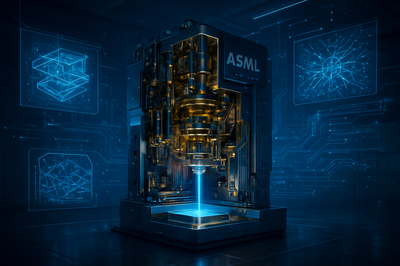
  • The Dawn of a New Era: Breakthroughs in Semiconductor Manufacturing Propel AI and Next-Gen Tech

    The Dawn of a New Era: Breakthroughs in Semiconductor Manufacturing Propel AI and Next-Gen Tech

    The semiconductor industry is on the cusp of a profound transformation, driven by an relentless pursuit of innovation in manufacturing techniques, materials science, and methodologies. As traditional scaling limits (often referred to as Moore's Law) become increasingly challenging, a new wave of advancements is emerging to overcome current manufacturing hurdles and dramatically enhance chip performance. These developments are not merely incremental improvements; they represent fundamental shifts that are critical for powering the next generation of artificial intelligence, high-performance computing, 5G/6G networks, and the burgeoning Internet of Things. The immediate significance of these breakthroughs is the promise of smaller, faster, more energy-efficient, and capable electronic devices across every sector, from consumer electronics to advanced industrial applications.

    Engineering the Future: Technical Leaps in Chip Fabrication

    The core of this revolution lies in several key technical areas, each pushing the boundaries of what's possible in chip design and production. At the forefront is advanced lithography, with Extreme Ultraviolet (EUV) technology now a mature process for sub-7 nanometer (nm) nodes. The industry is rapidly progressing towards High-Numerical Aperture (High-NA) EUV lithography, which aims to enable sub-2nm process nodes, further shrinking transistor dimensions. This is complemented by sophisticated multi-patterning techniques and advanced alignment stations, such as Nikon's Litho Booster 1000, which enhance overlay accuracy for complex 3D device structures, significantly improving process control and yield.

    Beyond shrinking transistors, 3D stacking and advanced packaging are redefining chip integration. Techniques like 3D stacking involve vertically integrating multiple semiconductor dies (chips) connected by through-silicon vias (TSVs), drastically reducing footprint and improving performance through shorter interconnects. Companies like Taiwan Semiconductor Manufacturing Company (NYSE: TSM) with its 3DFabric and Intel Corporation (NASDAQ: INTC) with Foveros are leading this charge. Furthermore, chiplet architectures and heterogeneous integration, where specialized "chiplets" are fabricated separately and then integrated into a single package, allow for unprecedented flexibility, scalability, and the combination of diverse technologies. This approach is evident in products from Advanced Micro Devices (NASDAQ: AMD) and NVIDIA Corporation (NASDAQ: NVDA), utilizing chiplets in their CPUs and GPUs, as well as Intel's Embedded Multi-die Interconnect Bridge (EMIB) technology.

    The fundamental building blocks of chips are also evolving with next-generation transistor architectures. The industry is transitioning from FinFETs to Gate-All-Around (GAA) transistors, including nanosheet and nanowire designs. GAA transistors offer superior electrostatic control by wrapping the gate around all sides of the channel, leading to significantly reduced leakage current, improved power efficiency, and enhanced performance scaling crucial for demanding applications like AI. Intel's RibbonFET and Samsung Electronics Co., Ltd.'s (KRX: 005930) Multi-Bridge Channel FET (MBCFET) are prime examples of this shift. These advancements differ from previous approaches by moving beyond the two-dimensional scaling limits of traditional silicon, embracing vertical integration, modular design, and novel material properties to achieve continued performance gains. Initial reactions from the AI research community and industry experts are overwhelmingly positive, recognizing these innovations as essential for sustaining the rapid pace of technological progress and enabling the next wave of AI capabilities.

    Corporate Battlegrounds: Reshaping the Tech Industry's Competitive Landscape

    The profound advancements in semiconductor manufacturing are creating new battlegrounds and strategic advantages across the tech industry, significantly impacting AI companies, tech giants, and innovative startups. Companies that can leverage these cutting-edge techniques and materials stand to gain immense competitive advantages, while others risk disruption.

    At the forefront of beneficiaries are the leading foundries and chip designers. Taiwan Semiconductor Manufacturing Company (NYSE: TSM) and Samsung Electronics Co., Ltd. (KRX: 005930), as pioneers in advanced process nodes like 3nm and 2nm, are experiencing robust demand driven by AI workloads. Similarly, fabless chip designers like NVIDIA Corporation (NASDAQ: NVDA), Advanced Micro Devices (NASDAQ: AMD), Marvell Technology, Inc. (NASDAQ: MRVL), Broadcom Inc. (NASDAQ: AVGO), and Qualcomm Incorporated (NASDAQ: QCOM) are exceptionally well-positioned due to their focus on high-performance GPUs, custom compute solutions, and AI-driven processors. The equipment manufacturers, most notably ASML Holding N.V. (NASDAQ: ASML) with its near-monopoly in EUV lithography, and Applied Materials, Inc. (NASDAQ: AMAT), providing crucial fabrication support, are indispensable enablers of this technological leap and are poised for substantial growth.

    The competitive implications for major AI labs and tech giants are particularly intense. Hyperscale cloud providers such as Alphabet Inc. (Google) (NASDAQ: GOOGL), Amazon.com, Inc. (NASDAQ: AMZN), Microsoft Corporation (NASDAQ: MSFT), and Meta Platforms, Inc. (NASDAQ: META) are investing hundreds of billions in capital expenditure to build their AI infrastructure. A significant trend is their strategic development of custom AI Application-Specific Integrated Circuits (ASICs), which grants them greater control over performance, cost, and supply chain. This move towards in-house chip design could potentially disrupt the market for off-the-shelf AI accelerators traditionally offered by semiconductor vendors. While these tech giants remain heavily reliant on advanced foundries for cutting-edge nodes, their vertical integration strategy is accelerating, elevating hardware control to a strategic asset as crucial as software innovation.

    For startups, the landscape presents both formidable challenges and exciting opportunities. The immense capital investment required for R&D and state-of-the-art fabrication facilities creates high barriers to entry for manufacturing. However, opportunities abound for new domestic semiconductor design startups, particularly those focusing on niche markets or specialized technologies. Government incentives, such as the U.S. CHIPS Act, are designed to foster these new players and build a more resilient domestic ecosystem. Programs like "Startups for Sustainable Semiconductors (S3)" are emerging to provide crucial mentoring and customer access, helping innovative AI-focused startups navigate the complexities of chip production. Ultimately, market positioning is increasingly defined by access to advanced fabrication capabilities, resilient supply chains, and continuous investment in R&D and technology leadership, all underpinned by the strategic importance of semiconductors in national security and economic dominance.

    A New Foundation: Broader Implications for AI and Society

    The ongoing revolution in semiconductor manufacturing extends far beyond the confines of fabrication plants, fundamentally reshaping the broader AI landscape and driving profound societal impacts. These advancements are not isolated technical feats but represent a critical enabler for the accelerating pace of AI development, creating a virtuous cycle where more powerful chips fuel AI breakthroughs, and AI, in turn, optimizes chip design and manufacturing.

    This era of "More than Moore" innovation, characterized by advanced packaging techniques like 2.5D and 3D stacking (e.g., TSMC's CoWoS used in NVIDIA's GPUs) and chiplet architectures, addresses the physical limits of traditional transistor scaling. By vertically integrating multiple layers of silicon and employing ultra-fine hybrid bonding, these methods dramatically shorten data travel distances, reducing latency and power consumption. This directly fuels the insatiable demand for computational power from cutting-edge AI, particularly large language models (LLMs) and generative AI, which require massive parallelization and computational efficiency. Furthermore, the rise of specialized AI chips – including GPUs, Tensor Processing Units (TPUs), Application-Specific Integrated Circuits (ASICs), and Neural Processing Units (NPUs) – optimized for specific AI workloads like image recognition and natural language processing, is a direct outcome of these manufacturing breakthroughs.

    The societal impacts are far-reaching. More powerful and efficient chips will accelerate the integration of AI into nearly every aspect of human life, from transforming healthcare and smart cities to enhancing transportation through autonomous vehicles and revolutionizing industrial automation. The semiconductor industry, projected to be a trillion-dollar market by 2030, is a cornerstone of global economic growth, with AI-driven hardware demand fueling significant R&D and capital expansion. Increased power efficiency from optimized chip designs also contributes to greater sustainability, making AI more cost-effective and environmentally responsible to operate at scale. This moment is comparable to previous AI milestones, such as the advent of GPUs for parallel processing or DeepMind's AlphaGo surpassing human champions in Go; it represents a foundational shift that enables the next wave of algorithmic breakthroughs and a "Cambrian explosion" in AI capabilities.

    However, these advancements also bring significant concerns. The complexity and cost of designing, manufacturing, and testing 3D stacked chips and chiplet systems are substantially higher than traditional monolithic designs. Geopolitical tensions exacerbate supply chain vulnerabilities, given the concentration of advanced chip production in a few regions, leading to a fierce global competition for technological dominance and raising concerns about national security. The immense energy consumption of advanced AI, particularly large data centers, presents environmental challenges, while the increasing capabilities of AI, powered by these chips, underscore ethical considerations related to bias, accountability, and responsible deployment. The global reliance on a handful of advanced chip manufacturers also creates potential power imbalances and technological dependence, necessitating careful navigation and sustained innovation to mitigate these risks.

    The Road Ahead: Future Developments and Horizon Applications

    The trajectory of semiconductor manufacturing points towards a future characterized by both continued refinement of existing technologies and the exploration of entirely new paradigms. In the near term, advanced lithography will continue its march, with High-NA EUV pushing towards sub-2nm and even Beyond EUV (BEUV) being explored. The transition to Gate-All-Around (GAA) transistors is becoming mainstream for sub-3nm nodes, promising enhanced power efficiency and performance through superior channel control. Simultaneously, 3D stacking and chiplet architectures will see significant expansion, with advanced packaging techniques like CoWoS experiencing increased capacity to meet the surging demand for high-performance computing (HPC) and AI accelerators. Automation and AI-driven optimization will become even more pervasive in fabs, leveraging machine learning for predictive maintenance, defect detection, and yield enhancement, thereby streamlining production and accelerating time-to-market.

    Looking further ahead, the industry will intensify its exploration of novel materials beyond silicon. Wide-bandgap semiconductors like Gallium Nitride (GaN) and Silicon Carbide (SiC) will become standard in high-power, high-frequency applications such as 5G/6G base stations, electric vehicles, and renewable energy systems. Long-term research will focus on 2D materials like graphene and molybdenum disulfide (MoS2) for ultra-thin, highly efficient transistors and flexible electronics. Methodologically, AI-enhanced design and verification will evolve, with generative AI automating complex design workflows from architecture to physical layout, significantly shortening design cycles. The trend towards heterogeneous computing integration, combining CPUs, GPUs, FPGAs, and specialized AI accelerators into unified architectures, will become the norm for optimizing diverse workloads.

    These advancements will unlock a vast array of potential applications. In AI, specialized chips will continue to power ever more sophisticated algorithms and deep learning models, enabling breakthroughs in areas from personalized medicine to autonomous decision-making. Advanced semiconductors are indispensable for the expansion of 5G and future 6G wireless communication, requiring high-speed transceivers and optical switches. Autonomous vehicles will rely on these chips for real-time sensor processing and enhanced safety. In healthcare, miniaturized, powerful processors will lead to more accurate wearable health monitors, implantable devices, and advanced lab-on-a-chip diagnostics. The Internet of Things (IoT) and smart cities will see seamless connectivity and processing at the edge, while flexible electronics and even silicon-based qubits for quantum computing remain exciting, albeit long-term, prospects.

    However, significant challenges loom. The rising capital intensity and costs of advanced fabs, now exceeding $30 billion, present a formidable barrier. Geopolitical fragmentation and the concentration of critical manufacturing in a few regions create persistent supply chain vulnerabilities and geopolitical risks. The industry also faces a talent shortage, particularly for engineers and technicians skilled in AI and advanced robotics. Experts predict continued market growth, potentially reaching $1 trillion by 2030, with AI and HPC remaining the primary drivers. There will be a sustained surge in demand for advanced packaging, a shift towards domain-specific and specialized chips facilitated by generative AI, and a strong trend towards the regionalization of manufacturing to enhance supply chain resilience. Sustainability will become an even greater imperative, with companies investing in energy-efficient production and green chemistry. The relentless pace of innovation, driven by the symbiotic relationship between AI and semiconductor technology, will continue to define the technological landscape for decades to come.

    The Microcosm's Macro Impact: A Concluding Assessment

    The semiconductor industry stands at a pivotal juncture, where a convergence of groundbreaking techniques, novel materials, and AI-driven methodologies is redefining the very essence of chip performance and manufacturing. From the precision of High-NA EUV lithography and the architectural ingenuity of 3D stacking and chiplet designs to the fundamental shift towards Gate-All-Around transistors and the integration of advanced materials like GaN and SiC, these developments are collectively overcoming long-standing manufacturing hurdles and extending the capabilities of digital technology far beyond the traditional limits of Moore's Law. The immediate significance is clear: an accelerated path to more powerful, energy-efficient, and intelligent devices that will underpin the next wave of innovation across AI, 5G/6G, IoT, and high-performance computing.

    This era marks a profound transformation for the tech industry, creating a highly competitive landscape where access to cutting-edge fabrication, robust supply chains, and strategic investments in R&D are paramount. While leading foundries and chip designers stand to benefit immensely, tech giants are increasingly pursuing vertical integration with custom silicon, challenging traditional market dynamics. For society, these advancements promise ubiquitous AI integration, driving economic growth, and enabling transformative applications in healthcare, transportation, and smart infrastructure. However, the journey is not without its complexities, including escalating costs, geopolitical vulnerabilities in the supply chain, and the critical need to address environmental impacts and ethical considerations surrounding powerful AI.

    In the grand narrative of AI history, the current advancements in semiconductor manufacturing represent a foundational shift, akin to the invention of the transistor itself or the advent of GPUs that first unlocked parallel processing for deep learning. They provide the essential hardware substrate upon which future algorithmic breakthroughs will be built, fostering a virtuous cycle of innovation. As we move into the coming weeks and months, the industry will be closely watching the deployment of High-NA EUV, the widespread adoption of GAA transistors, further advancements in 3D packaging capacity, and the continued integration of AI into every facet of chip design and production. The race for semiconductor supremacy is more than an economic competition; it is a determinant of technological leadership and societal progress in the digital age.


    This content is intended for informational purposes only and represents analysis of current AI developments.

    TokenRing AI delivers enterprise-grade solutions for multi-agent AI workflow orchestration, AI-powered development tools, and seamless remote collaboration platforms.
    For more information, visit https://www.tokenring.ai/.

  • Beyond Moore’s Law: Advanced Packaging and Lithography Unleash the Next Wave of AI Performance

    Beyond Moore’s Law: Advanced Packaging and Lithography Unleash the Next Wave of AI Performance

    The relentless pursuit of greater computational power for artificial intelligence is driving a fundamental transformation in semiconductor manufacturing, with advanced packaging and lithography emerging as the twin pillars supporting the next era of AI innovation. As traditional silicon scaling, often referred to as Moore's Law, faces physical and economic limitations, these sophisticated technologies are not merely extending chip capabilities but are indispensable for powering the increasingly complex demands of modern AI, from colossal large language models to pervasive edge computing. Their immediate significance lies in enabling unprecedented levels of performance, efficiency, and integration, fundamentally reshaping the design and production of AI-specific hardware and intensifying the strategic competition within the global tech industry.

    Innovations and Limitations: The Core of AI Semiconductor Evolution

    The AI semiconductor landscape is currently defined by a furious pace of innovation in both advanced packaging and lithography, each addressing critical bottlenecks while simultaneously presenting new challenges. In advanced packaging, the shift towards heterogeneous integration is paramount. Technologies such as 2.5D and 3D stacking, exemplified by Taiwan Semiconductor Manufacturing Company (TSMC) (TPE: 2330)'s CoWoS (Chip-on-Wafer-on-Substrate) variants, allow for the precise placement of multiple dies—including high-bandwidth memory (HBM) and specialized AI accelerators—on a single interposer or stacked vertically. This architecture dramatically reduces data transfer distances, alleviating the "memory wall" bottleneck that has traditionally hampered AI performance by ensuring ultra-fast communication between processing units and memory. Chiplet designs further enhance this modularity, enabling optimized cost and performance by allowing different components to be fabricated on their most suitable process nodes and improving manufacturing yields. Innovations like Intel Corporation (NASDAQ: INTC)'s EMIB (Embedded Multi-die Interconnect Bridge) and emerging Co-Packaged Optics (CPO) for AI networking are pushing the boundaries of integration, promising significant gains in efficiency and bandwidth by the late 2020s.

    However, these advancements come with inherent limitations. The complexity of integrating diverse materials and components in 2.5D and 3D packages introduces significant thermal management challenges, as denser integration generates more heat. The precise alignment required for vertical stacking demands incredibly tight tolerances, increasing manufacturing complexity and potential for defects. Yield management for these multi-die assemblies is also more intricate than for monolithic chips. Initial reactions from the AI research community and industry experts highlight these trade-offs, recognizing the immense performance gains but also emphasizing the need for robust thermal solutions, advanced testing methodologies, and more sophisticated design automation tools to fully realize the potential of these packaging innovations.

    Concurrently, lithography continues its relentless march towards finer features, with Extreme Ultraviolet (EUV) lithography at the forefront. EUV, utilizing 13.5nm wavelength light, enables the fabrication of transistors at 7nm, 5nm, 3nm, and even smaller nodes, which are absolutely critical for the density and efficiency required by modern AI processors. ASML Holding N.V. (NASDAQ: ASML) remains the undisputed leader, holding a near-monopoly on these highly complex and expensive machines. The next frontier is High-NA EUV, with a larger numerical aperture lens (0.55), promising to push feature sizes below 10nm, crucial for future 2nm and 1.4nm nodes like TSMC's A14 process, expected around 2027. While Deep Ultraviolet (DUV) lithography still plays a vital role for less critical layers and memory, the push for leading-edge AI chips is entirely dependent on EUV and its subsequent generations.

    The limitations in lithography primarily revolve around cost, complexity, and the fundamental physics of light. High-NA EUV systems, for instance, are projected to cost around $384 million each, making them an enormous capital expenditure for chip manufacturers. The extreme precision required, the specialized mask infrastructure, and the challenges of defect control at such minuscule scales contribute to significant manufacturing hurdles and impact overall yields. Emerging technologies like X-ray lithography (XRL) and nanoimprint lithography are being explored as potential long-term solutions to overcome some of these inherent limitations and to avoid the need for costly multi-patterning techniques at future nodes. Furthermore, AI itself is increasingly being leveraged within lithography processes, optimizing mask designs, predicting defects, and refining process parameters to improve efficiency and yield, demonstrating a symbiotic relationship between AI development and the tools that enable it.

    The Shifting Sands of AI Supremacy: Who Benefits from the Packaging and Lithography Revolution

    The advancements in advanced packaging and lithography are not merely technical feats; they are profound strategic enablers, fundamentally reshaping the competitive landscape for AI companies, tech giants, and burgeoning startups alike. At the forefront of benefiting are the major semiconductor foundries and Integrated Device Manufacturers (IDMs) like Taiwan Semiconductor Manufacturing Company (TSMC) (TPE: 2330), Intel Corporation (NASDAQ: INTC), and Samsung Electronics Co., Ltd. (KRX: 005930). TSMC's dominance in advanced packaging technologies such as CoWoS and InFO makes it an indispensable partner for virtually all leading AI chip designers. Similarly, Intel's EMIB and Foveros, and Samsung's I-Cube, are critical offerings that allow these giants to integrate diverse components into high-performance packages, solidifying their positions as foundational players in the AI supply chain. Their massive investments in expanding advanced packaging capacity underscore its strategic importance.

    AI chip designers and accelerator developers are also significant beneficiaries. NVIDIA Corporation (NASDAQ: NVDA), the undisputed leader in AI GPUs, heavily leverages 2.5D and 3D stacking with High Bandwidth Memory (HBM) for its cutting-edge accelerators like the H100, maintaining its competitive edge. Advanced Micro Devices, Inc. (NASDAQ: AMD) is a strong challenger, utilizing similar packaging strategies for its MI300 series. Hyperscalers and tech giants like Alphabet Inc. (Google) (NASDAQ: GOOGL) with its TPUs and Amazon.com, Inc. (NASDAQ: AMZN) with its Graviton and Trainium chips are increasingly relying on custom silicon, optimized through advanced packaging, to achieve superior performance-per-watt and cost efficiency for their vast AI workloads. This trend signals a broader move towards vertical integration where software, silicon, and packaging are co-designed for maximum impact.

    The competitive implications are stark. Advanced packaging has transcended its traditional role as a back-end process to become a core architectural enabler and a strategic differentiator. Companies with robust R&D and manufacturing capabilities in these areas gain substantial advantages, while those lagging risk being outmaneuvered. The shift towards modular, chiplet-based architectures, facilitated by advanced packaging, is a significant disruption. It allows for greater flexibility and could, to some extent, democratize chip design by enabling smaller startups to innovate by integrating specialized chiplets without the prohibitively high cost of designing an entire System-on-a-Chip (SoC) from scratch. However, this also introduces new challenges around chiplet interoperability and standardization. The "memory wall" – the bottleneck in data transfer between processing units and memory – is directly addressed by advanced packaging, which is crucial for the performance of large language models and generative AI.

    Market positioning is increasingly defined by access to and expertise in these advanced technologies. ASML Holding N.V. (NASDAQ: ASML), as the sole provider of leading-edge EUV lithography systems, holds an unparalleled strategic advantage, making it one of the most critical companies in the entire semiconductor ecosystem. Memory manufacturers like SK Hynix Inc. (KRX: 000660), Micron Technology, Inc. (NASDAQ: MU), and Samsung are experiencing surging demand for HBM, essential for high-performance AI accelerators. Outsourced Semiconductor Assembly and Test (OSAT) providers such as ASE Technology Holding Co., Ltd. (NYSE: ASX) and Amkor Technology, Inc. (NASDAQ: AMKR) are also becoming indispensable partners in the complex assembly of these advanced packages. Ultimately, the ability to rapidly innovate and scale production of AI chips through advanced packaging and lithography is now a direct determinant of strategic advantage and market leadership in the fiercely competitive AI race.

    A New Foundation for AI: Broader Implications and Looming Concerns

    The current revolution in advanced packaging and lithography is far more than an incremental improvement; it represents a foundational shift that is profoundly impacting the broader AI landscape and shaping its future trajectory. These hardware innovations are the essential bedrock upon which the next generation of AI systems, particularly the resource-intensive large language models (LLMs) and generative AI, are being built. By enabling unprecedented levels of performance, efficiency, and integration, they allow for the realization of increasingly complex neural network architectures and greater computational density, pushing the boundaries of what AI can achieve. This scaling is critical for everything from hyperscale data centers powering global AI services to compact, energy-efficient AI at the edge in devices and autonomous systems.

    This era of hardware innovation fits into the broader AI trend of moving beyond purely algorithmic breakthroughs to a symbiotic relationship between software and silicon. While previous AI milestones, such as the advent of deep learning algorithms or the widespread adoption of GPUs for parallel processing, were primarily driven by software and architectural insights, advanced packaging and lithography provide the physical infrastructure necessary to scale and deploy these innovations efficiently. They are directly addressing the "memory wall" bottleneck, a long-standing limitation in AI accelerator performance, by placing memory closer to processing units, leading to faster data access, higher bandwidth, and lower latency—all critical for the data-hungry demands of modern AI. This marks a departure from reliance solely on Moore's Law, as packaging has transitioned from a supportive back-end process to a core architectural enabler, integrating diverse chiplets and components into sophisticated "mini-systems."

    However, this transformative period is not without its concerns. The primary challenges revolve around the escalating cost and complexity of these advanced manufacturing processes. Designing, manufacturing, and testing 2.5D/3D stacked chips and chiplet systems are significantly more complex and expensive than traditional monolithic designs, leading to increased development costs and longer design cycles. The exorbitant price of High-NA EUV tools, for instance, translates into higher wafer costs. Thermal management is another critical issue; denser integration in advanced packages generates more localized heat, demanding innovative and robust cooling solutions to prevent performance degradation and ensure reliability.

    Perhaps the most pressing concern is the bottleneck in advanced packaging capacity. Technologies like TSMC's CoWoS are in such high demand that hyperscalers are pre-booking capacity up to eighteen months in advance, leaving smaller startups struggling to secure scarce slots and often facing idle wafers awaiting packaging. This capacity crunch can stifle innovation and slow the deployment of new AI technologies. Furthermore, geopolitical implications are significant, with export restrictions on advanced lithography machines to certain countries (e.g., China) creating substantial tensions and impacting their ability to produce cutting-edge AI chips. The environmental impact also looms large, as these advanced manufacturing processes become more energy-intensive and resource-demanding. Some experts even predict that the escalating demand for AI training could, in a decade or so, lead to power consumption exceeding globally available power, underscoring the urgent need for even more efficient models and hardware.

    The Horizon of AI Hardware: Future Developments and Expert Predictions

    The trajectory of advanced packaging and lithography points towards an even more integrated and specialized future for AI semiconductors. In the near-term, we can expect a continued rapid expansion of 2.5D and 3D integration, with a focus on improving hybrid bonding techniques to achieve even finer interconnect pitches and higher stack densities. The widespread adoption of chiplet architectures will accelerate, driven by the need for modularity, cost-effectiveness, and the ability to mix-and-match specialized components from different process nodes. This will necessitate greater standardization in chiplet interfaces and communication protocols to foster a more open and interoperable ecosystem. The commercialization and broader deployment of High-NA EUV lithography, particularly for sub-2nm process nodes, will be a critical near-term development, enabling the next generation of ultra-dense transistors.

    Looking further ahead, long-term developments include the exploration of novel materials and entirely new integration paradigms. Co-Packaged Optics (CPO) will likely become more prevalent, integrating optical interconnects directly into advanced packages to overcome electrical bandwidth limitations for inter-chip and inter-system communication, crucial for exascale AI systems. Experts predict the emergence of "system-on-wafer" or "system-in-package" solutions that blur the lines between chip and system, creating highly integrated, application-specific AI engines. Research into alternative lithography methods like X-ray lithography and nanoimprint lithography could offer pathways beyond the physical limits of current EUV technology, potentially enabling even finer features without the complexities of multi-patterning.

    The potential applications and use cases on the horizon are vast. More powerful and efficient AI chips will enable truly ubiquitous AI, powering highly autonomous vehicles with real-time decision-making capabilities, advanced personalized medicine through rapid genomic analysis, and sophisticated real-time simulation and digital twin technologies. Generative AI models will become even larger and more capable, moving beyond text and images to create entire virtual worlds and complex interactive experiences. Edge AI devices, from smart sensors to robotics, will gain unprecedented processing power, enabling complex AI tasks locally without constant cloud connectivity, enhancing privacy and reducing latency.

    However, several challenges need to be addressed to fully realize this future. Beyond the aforementioned cost and thermal management issues, the industry must tackle the growing complexity of design and verification for these highly integrated systems. New Electronic Design Automation (EDA) tools and methodologies will be essential. Supply chain resilience and diversification will remain critical, especially given geopolitical tensions. Furthermore, the energy consumption of AI training and inference, already a concern, will demand continued innovation in energy-efficient hardware architectures and algorithms to ensure sustainability. Experts predict a future where hardware and software co-design becomes even more intertwined, with AI itself playing a crucial role in optimizing chip design, manufacturing processes, and even material discovery. The industry is moving towards a holistic approach where every layer of the technology stack, from atoms to algorithms, is optimized for AI.

    The Indispensable Foundation: A Wrap-up on AI's Hardware Revolution

    The advancements in advanced packaging and lithography are not merely technical footnotes in the story of AI; they are the bedrock upon which the future of artificial intelligence is being constructed. The key takeaway is clear: as traditional methods of scaling transistor density reach their physical and economic limits, these sophisticated hardware innovations have become indispensable for continuing the exponential growth in computational power required by modern AI. They are enabling heterogeneous integration, alleviating the "memory wall" with High Bandwidth Memory, and pushing the boundaries of miniaturization with Extreme Ultraviolet lithography, thereby unlocking unprecedented performance and efficiency for everything from generative AI to edge computing.

    This development marks a pivotal moment in AI history, akin to the introduction of the GPU for parallel processing or the breakthroughs in deep learning algorithms. Unlike those milestones, which were largely software or architectural, advanced packaging and lithography provide the fundamental physical infrastructure that allows these algorithmic and architectural innovations to be realized at scale. They represent a strategic shift where the "back-end" of chip manufacturing has become a "front-end" differentiator, profoundly impacting competitive dynamics among tech giants, fostering new opportunities for innovation, and presenting significant challenges related to cost, complexity, and supply chain bottlenecks.

    The long-term impact will be a world increasingly permeated by intelligent systems, powered by chips that are more integrated, specialized, and efficient than ever before. This hardware revolution will enable AI to tackle problems of greater complexity, operate with higher autonomy, and integrate seamlessly into every facet of our lives. In the coming weeks and months, we should watch for continued announcements regarding expanded advanced packaging capacity from leading foundries, further refinements in High-NA EUV deployment, and the emergence of new chiplet standards. The race for AI supremacy will increasingly be fought not just in algorithms and data, but in the very atoms and architectures that form the foundation of intelligent machines.


    This content is intended for informational purposes only and represents analysis of current AI developments.

    TokenRing AI delivers enterprise-grade solutions for multi-agent AI workflow orchestration, AI-powered development tools, and seamless remote collaboration platforms.
    For more information, visit https://www.tokenring.ai/.

  • ASML: The Unseen Architect Powering the AI Revolution and Beyond

    ASML: The Unseen Architect Powering the AI Revolution and Beyond

    Lithography, the intricate process of etching microscopic patterns onto silicon wafers, stands as the foundational cornerstone of modern semiconductor manufacturing. Without this highly specialized technology, the advanced microchips that power everything from our smartphones to sophisticated artificial intelligence systems would simply not exist. At the very heart of this critical industry lies ASML Holding N.V. (NASDAQ: ASML), a Dutch multinational company that has emerged as the undisputed leader and sole provider of the most advanced lithography equipment, making it an indispensable enabler for the entire global semiconductor sector.

    ASML's technological prowess, particularly its pioneering work in Extreme Ultraviolet (EUV) lithography, has positioned it as a gatekeeper to the future of computing. Its machines are not merely tools; they are the engines driving Moore's Law, allowing chipmakers to continuously shrink transistors and pack billions of them onto a single chip. This relentless miniaturization fuels the exponential growth in processing power and efficiency, directly underpinning breakthroughs in artificial intelligence, high-performance computing, and a myriad of emerging technologies. As of November 2025, ASML's innovations are more critical than ever, dictating the pace of technological advancement and shaping the competitive landscape for chip manufacturers worldwide.

    Precision Engineering: The Technical Marvels of Modern Lithography

    The journey of creating a microchip begins with lithography, a process akin to projecting incredibly detailed blueprints onto a silicon wafer. This involves coating the wafer with a light-sensitive material (photoresist), exposing it to a pattern of light through a mask, and then etching the pattern into the wafer. This complex sequence is repeated dozens of times to build the multi-layered structures of an integrated circuit. ASML's dominance stems from its mastery of Deep Ultraviolet (DUV) and, more crucially, Extreme Ultraviolet (EUV) lithography.

    EUV lithography represents a monumental leap forward, utilizing light with an incredibly short wavelength of 13.5 nanometers – approximately 14 times shorter than the DUV light used in previous generations. This ultra-short wavelength allows for the creation of features on chips that are mere nanometers in size, pushing the boundaries of what was previously thought possible. ASML is the sole global manufacturer of these highly sophisticated EUV machines, which employ a complex system of mirrors in a vacuum environment to focus and project the EUV light. This differs significantly from older DUV systems that use lenses and longer wavelengths, limiting their ability to resolve the extremely fine features required for today's most advanced chips (7nm, 5nm, 3nm, and upcoming sub-2nm nodes). Initial reactions from the semiconductor research community and industry experts heralded EUV as a necessary, albeit incredibly challenging, breakthrough to continue Moore's Law, overcoming the physical limitations of DUV and multi-patterning techniques.

    Further solidifying its leadership, ASML is already pushing the boundaries with its next-generation High Numerical Aperture (High-NA) EUV systems, known as EXE platforms. These machines boast an NA of 0.55, a significant increase from the 0.33 NA of current EUV systems. This higher numerical aperture will enable even smaller transistor features and improved resolution, effectively doubling the density of transistors that can be printed on a chip. While current EUV systems are enabling high-volume manufacturing of 3nm and 2nm chips, High-NA EUV is critical for the development and eventual high-volume production of future sub-2nm nodes, expected to ramp up in 2025-2026. This continuous innovation ensures ASML remains at the forefront, providing the tools necessary for the next wave of chip advancements.

    ASML's Indispensable Role: Shaping the Semiconductor Competitive Landscape

    ASML's technological supremacy has profound implications for the entire semiconductor ecosystem, directly influencing the competitive dynamics among the world's leading chip manufacturers. Companies that rely on cutting-edge process nodes to produce their chips are, by necessity, ASML's primary customers.

    The most significant beneficiaries of ASML's advanced lithography, particularly EUV, are the major foundry operators and integrated device manufacturers (IDMs) such as Taiwan Semiconductor Manufacturing Company (TSMC) (NYSE: TSM), Samsung Electronics Co., Ltd. (KRX: 005930), and Intel Corporation (NASDAQ: INTC). These tech giants are locked in a fierce race to produce the fastest, most power-efficient chips, and access to ASML's EUV machines is a non-negotiable requirement for staying competitive at the leading edge. Without ASML's technology, these companies would be unable to fabricate the advanced processors, memory, and specialized AI accelerators that define modern computing.

    This creates a unique market positioning for ASML, effectively making it a strategic partner rather than just a supplier. Its technology enables its customers to differentiate their products, gain market share, and drive innovation. For example, TSMC's ability to produce chips for Apple, Qualcomm, and Nvidia at the most advanced nodes is directly tied to its investment in ASML's EUV fleet. Similarly, Samsung's foundry business and its own memory production heavily rely on ASML. Intel, having lagged in process technology for some years, is now aggressively investing in ASML's latest EUV and High-NA EUV systems to regain its competitive edge and execute its "IDM 2.0" strategy.

    The competitive implications are stark: companies with limited or no access to ASML's most advanced equipment risk falling behind in the race for performance and efficiency. This could lead to a significant disruption to existing product roadmaps for those unable to keep pace, potentially impacting their ability to serve high-growth markets like AI, 5G, and autonomous vehicles. ASML's strategic advantage is not just in its hardware but also in its deep relationships with these industry titans, collaboratively pushing the boundaries of what's possible in semiconductor manufacturing.

    The Broader Significance: Fueling the Digital Future

    ASML's role in lithography transcends mere equipment supply; it is a linchpin in the broader technological landscape, directly influencing global trends and the pace of digital transformation. Its advancements are critical for the continued validity of Moore's Law, which, despite numerous predictions of its demise, continues to be extended thanks to innovations like EUV and High-NA EUV. This sustained ability to miniaturize transistors is the bedrock upon which the entire digital economy is built.

    The impacts are far-reaching. The exponential growth in data and the demand for increasingly sophisticated AI models require unprecedented computational power. ASML's technology enables the fabrication of the high-density, low-power chips essential for training large language models, powering advanced machine learning algorithms, and supporting the infrastructure for edge AI. Without these advanced chips, the AI revolution would face significant bottlenecks, slowing progress across industries from healthcare and finance to automotive and entertainment.

    However, ASML's critical position also raises potential concerns. Its near-monopoly on advanced EUV technology grants it significant geopolitical leverage. The ability to control access to these machines can become a tool in international trade and technology disputes, as evidenced by export control restrictions on sales to certain regions. This concentration of power in one company, albeit a highly innovative one, underscores the fragility of the global supply chain for critical technologies. Comparisons to previous AI milestones, such as the development of neural networks or the rise of deep learning, often focus on algorithmic breakthroughs. However, ASML's contribution is more fundamental, providing the physical infrastructure that makes these algorithmic advancements computationally feasible and economically viable.

    The Horizon of Innovation: What's Next for Lithography

    Looking ahead, the trajectory of lithography technology, largely dictated by ASML, promises even more remarkable advancements and will continue to shape the future of computing. The immediate focus is on the widespread adoption and optimization of High-NA EUV technology.

    Expected near-term developments include the deployment of ASML's High-NA EUV (EXE:5000 and EXE:5200) systems into research and development facilities, with initial high-volume manufacturing expected around 2025-2026. These systems will enable chipmakers to move beyond 2nm nodes, paving the way for 1.5nm and even 1nm process technologies. Potential applications and use cases on the horizon are vast, ranging from even more powerful and energy-efficient AI accelerators, enabling real-time AI processing at the edge, to advanced quantum computing chips and next-generation memory solutions. These advancements will further shrink device sizes, leading to more compact and powerful electronics across all sectors.

    However, significant challenges remain. The cost of developing and operating these cutting-edge lithography systems is astronomical, pushing up the overall cost of chip manufacturing. The complexity of the EUV ecosystem, from the light source to the intricate mirror systems and precise alignment, demands continuous innovation and collaboration across the supply chain. Furthermore, the industry faces the physical limits of silicon and light-based lithography, prompting research into alternative patterning techniques like directed self-assembly or novel materials. Experts predict that while High-NA EUV will extend Moore's Law for another decade, the industry will increasingly explore hybrid approaches combining advanced lithography with 3D stacking and new transistor architectures to continue improving performance and efficiency.

    A Pillar of Progress: ASML's Enduring Legacy

    In summary, lithography technology, with ASML at its vanguard, is not merely a component of semiconductor manufacturing; it is the very engine driving the digital age. ASML's unparalleled leadership in both DUV and, critically, EUV lithography has made it an indispensable partner for the world's leading chipmakers, enabling the continuous miniaturization of transistors that underpin Moore's Law and fuels the relentless pace of technological progress.

    This development's significance in AI history cannot be overstated. While AI research focuses on algorithms and models, ASML provides the fundamental hardware infrastructure that makes advanced AI feasible. Its technology directly enables the high-performance, energy-efficient chips required for training and deploying complex AI systems, from large language models to autonomous driving. Without ASML's innovations, the current AI revolution would be severely constrained, highlighting its profound and often unsung impact.

    Looking ahead, the ongoing rollout of High-NA EUV technology and ASML's continued research into future patterning solutions will be crucial to watch in the coming weeks and months. The semiconductor industry's ability to meet the ever-growing demand for more powerful and efficient chips—a demand largely driven by AI—rests squarely on the shoulders of companies like ASML. Its innovations will continue to shape not just the tech industry, but the very fabric of our digitally connected world for decades to come.


    This content is intended for informational purposes only and represents analysis of current AI developments.

    TokenRing AI delivers enterprise-grade solutions for multi-agent AI workflow orchestration, AI-powered development tools, and seamless remote collaboration platforms.
    For more information, visit https://www.tokenring.ai/.

  • ASML Supercharges South Korea: New Headquarters and EUV R&D Cement Global Lithography Leadership

    ASML Supercharges South Korea: New Headquarters and EUV R&D Cement Global Lithography Leadership

    In a monumental strategic maneuver, ASML Holding N.V. (NASDAQ: ASML), the Dutch technology giant and the world's sole manufacturer of extreme ultraviolet (EUV) lithography machines, has significantly expanded its footprint in South Korea. This pivotal move, centered around the establishment of a comprehensive new headquarters campus in Hwaseong and a massive joint R&D initiative with Samsung Electronics (KRX: 005930), is set to profoundly bolster global lithography capabilities and solidify South Korea's indispensable role in the advanced semiconductor ecosystem. As of November 2025, the Hwaseong campus is fully operational, providing crucial localized support, while the groundbreaking R&D collaboration with Samsung is actively progressing, albeit with a re-evaluated location strategy for optimal acceleration.

    This expansion is far more than a simple investment; it represents a deep commitment to the future of advanced chip manufacturing, which is the bedrock of artificial intelligence, high-performance computing, and next-generation technologies. By bringing critical repair, training, and cutting-edge research facilities closer to its major customers, ASML is not only enhancing the resilience of the global semiconductor supply chain but also accelerating the development of the ultra-fine processes essential for the sub-2 nanometer era, directly impacting the capabilities of AI hardware worldwide.

    Unpacking the Technical Core: Localized Support Meets Next-Gen EUV Innovation

    ASML's strategic build-out in South Korea is multifaceted, addressing both immediate operational needs and long-term technological frontiers. The new Hwaseong campus, a 240 billion won (approximately $182 million) investment, became fully operational by the end of 2024. This expansive facility houses a Local Repair Center (LRC), also known as a Remanufacturing Center, designed to service ASML's highly complex equipment using an increasing proportion of domestically produced parts—aiming to boost local sourcing from 10% to 50%. This localized repair capability drastically reduces downtime for crucial lithography machines, a critical factor for chipmakers like Samsung and SK Hynix (KRX: 000660).

    Complementing this is a state-of-the-art Global Training Center, which, along with a second EUV training center inaugurated in Yongin City, is set to increase ASML's global EUV lithography technician training capacity by 30%. These centers are vital for cultivating a skilled workforce capable of operating and maintaining the highly sophisticated EUV and DUV (Deep Ultraviolet) systems. An Experience Center also forms part of the Hwaseong campus, engaging the local community and showcasing semiconductor technology.

    The spearhead of ASML's innovation push in South Korea is the joint R&D initiative with Samsung Electronics, a monumental 1 trillion won ($760 million) investment focused on developing "ultra-microscopic" level semiconductor production technology using next-generation EUV equipment. While initial plans for a specific Hwaseong site were re-evaluated in April 2025, ASML and Samsung are actively exploring alternative locations, potentially within an existing Samsung campus, to expedite the establishment of this critical R&D hub. This center is specifically geared towards High-NA EUV (EXE systems), which boast a numerical aperture (NA) of 0.55, a significant leap from the 0.33 NA of previous NXE systems. This enables the etching of circuits 1.7 times finer, achieving an 8 nm resolution—a dramatic improvement over the 13 nm resolution of older EUV tools. This technological leap is indispensable for manufacturing chips at the 2 nm node and beyond, pushing the boundaries of what's possible in chip density and performance. Samsung has already deployed its first High-NA EUV equipment (EXE:5000) at its Hwaseong campus in March 2025, with plans for two more by mid-2026, while SK Hynix has also installed High-NA EUV systems at its M16 fabrication plant.

    These advancements represent a significant departure from previous industry reliance on centralized support from ASML's headquarters in the Netherlands. The localized repair and training capabilities minimize logistical hurdles and foster indigenous expertise. More profoundly, the joint R&D center signifies a deeper co-development partnership, moving beyond a mere customer-supplier dynamic to accelerate innovation cycles for advanced nodes, ensuring the rapid deployment of technologies like High-NA EUV that are critical for future high-performance computing. Initial reactions from the AI research community and industry experts have been overwhelmingly positive, recognizing these developments as fundamental enablers for the next generation of AI chips and a crucial step towards the sub-2nm manufacturing era.

    Reshaping the AI and Tech Landscape: Beneficiaries and Competitive Shifts

    ASML's deepened presence in South Korea is poised to create a ripple effect across the global technology industry, directly benefiting key players and reshaping competitive dynamics. Unsurprisingly, the most immediate and substantial beneficiaries are ASML's primary South Korean customers, Samsung Electronics (KRX: 005930) and SK Hynix (KRX: 000660). These companies, which collectively account for a significant portion of ASML's worldwide sales, gain priority access to the latest EUV and High-NA EUV technologies, direct collaboration with ASML engineers, and enhanced local support and training. This accelerated access is paramount for their ability to produce advanced logic chips and high-bandwidth memory (HBM), both of which are critical components for cutting-edge AI applications. Samsung, in particular, anticipates a significant edge in the race for next-generation chip production through this partnership, aiming for 2nm commercialization by 2025. Furthermore, SK Hynix's collaboration with ASML on hydrogen recycling technology for EUV systems underscores a growing industry focus on energy efficiency, a crucial factor for power-intensive AI data centers.

    Beyond the foundries, global AI chip designers such as Nvidia, Intel (NASDAQ: INTC), and Qualcomm (NASDAQ: QCOM) will indirectly benefit immensely. As these companies rely on advanced foundries like Samsung (and TSMC) to fabricate their sophisticated AI chips, ASML's enhanced capabilities in South Korea contribute to a more robust and advanced manufacturing ecosystem, enabling faster development and production of their cutting-edge AI silicon. Similarly, major cloud providers and hyperscalers like Google (NASDAQ: GOOGL), Amazon Web Services (NASDAQ: AMZN), and Microsoft (NASDAQ: MSFT), which are increasingly developing custom AI chips (e.g., Google's TPUs, AWS's Trainium/Inferentia, Microsoft's Azure Maia/Cobalt), will find their efforts bolstered. ASML's technology, facilitated through its foundry partners, empowers the production of these specialized AI solutions, leading to more powerful, efficient, and cost-effective computing resources for AI development and deployment. The invigorated South Korean semiconductor ecosystem, driven by ASML's investments, also creates a fertile ground for local AI and deep tech startups, fostering a vibrant innovation environment.

    Competitively, ASML's expansion further entrenches its near-monopoly on EUV lithography, solidifying its position as an "indispensable enabler" and "arbiter of progress" in advanced chip manufacturing. By investing in next-generation High-NA EUV development and strengthening ties with key customers in South Korea—now ASML's largest market, accounting for 40% of its Q1 2025 revenue—ASML raises the entry barriers for any potential competitor, securing its central role in the AI revolution. This move also intensifies foundry competition, particularly in the ongoing rivalry between Samsung, TSMC, and Intel for leadership in producing sub-2nm chips. The localized availability of ASML's most advanced lithography tools will accelerate the design and production cycles of specialized AI chips, fueling an "AI-driven ecosystem" and an "unprecedented semiconductor supercycle." Potential disruptions include the accelerated obsolescence of current hardware as High-NA EUV enables sub-2nm chips, and a potential shift towards custom AI silicon by tech giants, which could impact the market share of general-purpose GPUs for specific AI workloads.

    Wider Significance: Fueling the AI Revolution and Global Tech Sovereignty

    ASML's strategic expansion in South Korea transcends mere corporate investment; it is a critical development that profoundly shapes the broader AI landscape and global technological trends. Advanced chips are the literal building blocks of the AI revolution, enabling the massive computational power required for large language models, complex neural networks, and myriad AI applications from autonomous vehicles to personalized medicine. By accelerating the availability and refinement of cutting-edge lithography, ASML is directly fueling the progress of AI, making smaller, faster, and more energy-efficient AI processors a reality. This fits perfectly into the current trajectory of AI, which demands ever-increasing computational density and power efficiency to achieve new breakthroughs.

    The impacts are far-reaching. Firstly, it significantly enhances global semiconductor supply chain resilience. The establishment of local repair and remanufacturing centers in South Korea reduces reliance on a single point of failure (the Netherlands) for critical maintenance, a lesson learned from recent geopolitical and logistical disruptions. Secondly, it fosters vital talent development. The new training centers are cultivating a highly skilled workforce within South Korea, ensuring a continuous supply of expertise for the highly specialized semiconductor and AI industries. This localized talent pool is crucial for sustaining leadership in advanced manufacturing. Thirdly, ASML's investment carries significant geopolitical weight. It strengthens the "semiconductor alliance" between South Korea and the Netherlands, reinforcing technological sovereignty efforts among allied nations and serving as a strategic move for geographical diversification amidst ongoing global trade tensions and export restrictions.

    Compared to previous AI milestones, such as the development of early neural networks or the rise of deep learning, ASML's contribution is foundational. While AI algorithms and software drive intelligence, it is the underlying hardware, enabled by ASML's lithography, that provides the raw processing power. This expansion is a milestone in hardware enablement, arguably as critical as any software breakthrough, as it dictates the physical limits of what AI can achieve. Concerns, however, remain around the concentration of such critical technology in a single company, and the potential for geopolitical tensions to impact supply chains despite diversification efforts. The sheer cost and complexity of EUV technology also present high barriers to entry, further solidifying ASML's near-monopoly and the competitive advantage it bestows upon its primary customers.

    The Road Ahead: Future Developments and AI's Next Frontier

    Looking ahead, ASML's strategic investments in South Korea lay the groundwork for several key developments in the near and long term. In the near term, the full operationalization of the Hwaseong campus's repair and training facilities will lead to immediate improvements in chip production efficiency for Samsung and SK Hynix, reducing downtime and accelerating throughput. The ongoing joint R&D initiative with Samsung, despite the relocation considerations, is expected to make significant strides in developing and deploying next-generation High-NA EUV for sub-2nm processes. This means we can anticipate the commercialization of even more powerful and efficient chips in the very near future, potentially driving new generations of AI accelerators and specialized processors.

    Longer term, ASML plans to open an additional office in Yongin by 2027, focusing on technical support, maintenance, and repair near the SK Semiconductor Industrial Complex. This further decentralization of support will enhance responsiveness for another major customer. The continuous advancements in EUV technology, particularly the push towards High-NA EUV and beyond, will unlock new frontiers in chip design, enabling even denser and more complex integrated circuits. These advancements will directly translate into more powerful AI models, more efficient edge AI deployments, and entirely new applications in fields like quantum computing, advanced robotics, and personalized healthcare.

    However, challenges remain. The intense demand for skilled talent in the semiconductor industry will necessitate continued investment in education and training programs, both by ASML and its partners. Maintaining the technological lead in lithography requires constant innovation and significant R&D expenditure. Experts predict that the semiconductor market will continue its rapid expansion, projected to double within a decade, driven by AI, automotive innovation, and energy transition. ASML's proactive investments are designed to meet this escalating global demand, ensuring it remains the "foundational enabler" of the digital economy. The next few years will likely see a fierce race to master the 2nm and sub-2nm nodes, with ASML's South Korean expansion playing a pivotal role in this technological arms race.

    A New Era for Global Chipmaking and AI Advancement

    ASML's strategic expansion in South Korea marks a pivotal moment in the history of advanced semiconductor manufacturing and, by extension, the trajectory of artificial intelligence. The completion of the Hwaseong campus and the ongoing, high-stakes joint R&D with Samsung represent a deep, localized commitment that moves beyond traditional customer-supplier relationships. Key takeaways include the significant enhancement of localized support for critical lithography equipment, a dramatic acceleration in the development of next-generation High-NA EUV technology, and the strengthening of South Korea's position as a global semiconductor and AI powerhouse.

    This development's significance in AI history cannot be overstated. It directly underpins the physical capabilities required for the exponential growth of AI, enabling the creation of the faster, smaller, and more energy-efficient chips that power everything from advanced neural networks to sophisticated data centers. Without these foundational lithography advancements, the theoretical breakthroughs in AI would lack the necessary hardware to become practical realities. The long-term impact will be seen in the continued miniaturization and increased performance of all electronic devices, pushing the boundaries of what AI can achieve and integrating it more deeply into every facet of society.

    In the coming weeks and months, industry observers will be closely watching the progress of the joint R&D center with Samsung, particularly regarding its finalized location and the initial fruits of its ultra-fine process development. Further deployments of High-NA EUV systems by Samsung and SK Hynix will also be key indicators of the pace of advancement into the sub-2nm era. ASML's continued investment in global capacity and R&D, epitomized by this South Korean expansion, underscores its indispensable role in shaping the future of technology and solidifying its position as the arbiter of progress in the AI-driven world.


    This content is intended for informational purposes only and represents analysis of current AI developments.

    TokenRing AI delivers enterprise-grade solutions for multi-agent AI workflow orchestration, AI-powered development tools, and seamless remote collaboration platforms.
    For more information, visit https://www.tokenring.ai/.

  • The Future of Semiconductor Manufacturing: Trends and Innovations

    The Future of Semiconductor Manufacturing: Trends and Innovations

    The semiconductor industry stands at the precipice of an unprecedented era of growth and innovation, poised to shatter the $1 trillion market valuation barrier by 2030. This monumental expansion, often termed a "super cycle," is primarily fueled by the insatiable global demand for advanced computing, particularly from the burgeoning field of Artificial Intelligence. As of November 11, 2025, the industry is navigating a complex landscape shaped by relentless technological breakthroughs, evolving market imperatives, and significant geopolitical realignments, all converging to redefine the very foundations of modern technology.

    This transformative period is characterized by a dual revolution: the continued push for miniaturization alongside a strategic pivot towards novel architectures and materials. Beyond merely shrinking transistors, manufacturers are embracing advanced packaging, exploring exotic new compounds, and integrating AI into the very fabric of chip design and production. These advancements are not just incremental improvements; they represent fundamental shifts that promise to unlock the next generation of AI systems, autonomous technologies, and a myriad of connected devices, cementing semiconductors as the indispensable engine of the 21st-century economy.

    Beyond the Silicon Frontier: Engineering the Next Generation of Intelligence

    The relentless pursuit of computational supremacy, primarily driven by the demands of artificial intelligence and high-performance computing, has propelled the semiconductor industry into an era of profound technical innovation. At the core of this transformation are revolutionary advancements in transistor architecture, lithography, advanced packaging, and novel materials, each representing a significant departure from traditional silicon-centric manufacturing.

    One of the most critical evolutions in transistor design is the Gate-All-Around (GAA) transistor, exemplified by Samsung's (KRX:005930) Multi-Bridge-Channel FET (MBCFET™) and Intel's (NASDAQ:INTC) upcoming RibbonFET. Unlike their predecessors, FinFETs, where the gate controls the channel from three sides, GAA transistors completely encircle the channel, typically in the form of nanosheets or nanowires. This "all-around" gate design offers superior electrostatic control, drastically reducing leakage currents and mitigating short-channel effects that become prevalent at sub-5nm nodes. Furthermore, GAA nanosheets provide unprecedented flexibility in adjusting channel width, allowing for more precise tuning of performance and power characteristics—a crucial advantage for energy-hungry AI workloads. Industry reception is overwhelmingly positive, with major foundries rapidly transitioning to GAA architectures as the cornerstone for future sub-3nm process nodes.

    Complementing these transistor innovations is the cutting-edge High-Numerical Aperture (High-NA) Extreme Ultraviolet (EUV) lithography. ASML's (AMS:ASML) TWINSCAN EXE:5000, with its 0.55 NA lens, represents a significant leap from current 0.33 NA EUV systems. This higher NA enables a resolution of 8 nm, allowing for the printing of significantly smaller features and nearly triple the transistor density compared to existing EUV. While current EUV is crucial for 7nm and 5nm nodes, High-NA EUV is indispensable for the 2nm node and beyond, potentially eliminating the need for complex and costly multi-patterning techniques. Intel received the first High-NA EUV modules in December 2023, signaling its commitment to leading the charge. While the immense cost and complexity pose challenges—with some reports suggesting TSMC (NYSE:TSM) and Samsung might strategically delay its full adoption for certain nodes—the industry broadly recognizes High-NA EUV as a critical enabler for the next wave of miniaturization essential for advanced AI chips.

    As traditional scaling faces physical limits, advanced packaging has emerged as a parallel and equally vital pathway to enhance performance. Techniques like 3D stacking, which vertically integrates multiple dies using Through-Silicon Vias (TSVs), dramatically reduce data travel distances, leading to faster data transfer, improved power efficiency, and a smaller footprint. This is particularly evident in High Bandwidth Memory (HBM), a form of 3D-stacked DRAM that has become indispensable for AI accelerators and HPC due to its unparalleled bandwidth and power efficiency. Companies like SK Hynix (KRX:000660), Samsung, and Micron (NASDAQ:MU) are aggressively expanding HBM production to meet surging AI data center demand. Simultaneously, chiplets are revolutionizing chip design by breaking monolithic System-on-Chips (SoCs) into smaller, modular components. This approach enhances yields, reduces costs by allowing different process nodes for different functions, and offers greater design flexibility. Standards like UCIe are fostering an open chiplet ecosystem, enabling custom-tailored solutions for specific AI performance and power requirements.

    Beyond silicon, the exploration of novel materials is opening new frontiers. Wide bandgap semiconductors like Gallium Nitride (GaN) and Silicon Carbide (SiC) are rapidly replacing silicon in power electronics. GaN, with its superior electron mobility and breakdown strength, enables faster switching, higher power density, and greater efficiency in applications ranging from EV chargers to 5G base stations. SiC, boasting even higher thermal conductivity and breakdown voltage, is pivotal for high-power devices in electric vehicles and renewable energy systems. Further out, 2D materials such as Molybdenum Disulfide (MoS2) and Indium Selenide (InSe) are showing immense promise for ultra-thin, high-mobility transistors that could push past silicon's theoretical limits, particularly for future low-power AI at the edge. While still facing manufacturing challenges, recent advancements in wafer-scale fabrication of InSe are seen as a major step towards a post-silicon future.

    The AI research community and industry experts view these technical shifts with immense optimism, recognizing their fundamental role in accelerating AI capabilities. The ability to achieve superior computational power, data throughput, and energy efficiency through GAA, High-NA EUV, and advanced packaging is deemed critical for advancing large language models, autonomous systems, and ubiquitous edge AI. However, concerns about the immense cost of development and deployment, particularly for High-NA EUV, hint at potential industry consolidation, where only the leading foundries with significant capital can compete at the cutting edge.

    Corporate Battlegrounds: Who Wins and Loses in the Chip Revolution

    The seismic shifts in semiconductor manufacturing are fundamentally reshaping the competitive landscape for tech giants, AI companies, and nimble startups alike. The ability to harness innovations like GAA transistors, High-NA EUV, advanced packaging, and novel materials is becoming the ultimate determinant of market leadership and strategic advantage.

    Leading the charge in manufacturing are the pure-play foundries and Integrated Device Manufacturers (IDMs). Taiwan Semiconductor Manufacturing Company (NYSE:TSM), already a dominant force, is heavily invested in GAA and advanced packaging technologies like CoWoS and InFO, ensuring its continued pivotal role for virtually all major chip designers. Samsung Electronics Co., Ltd. (KRX:005930), as both an IDM and foundry, is fiercely competing with TSMC, notably with its MBCFET™ GAA technology. Meanwhile, Intel Corporation (NASDAQ:INTC) is making aggressive moves to reclaim process leadership, being an early adopter of ASML's High-NA EUV scanner and developing its own RibbonFET GAA technology and advanced packaging solutions like EMIB. These three giants are locked in a high-stakes "2nm race," where success in mastering these cutting-edge processes will dictate who fabricates the next generation of high-performance chips.

    The impact extends profoundly to chip designers and AI innovators. Companies like NVIDIA Corporation (NASDAQ:NVDA), the undisputed leader in AI GPUs, and Advanced Micro Devices, Inc. (NASDAQ:AMD), a strong competitor in CPUs, GPUs, and AI accelerators, are heavily reliant on these advanced manufacturing and packaging techniques to power their increasingly complex and demanding chips. Tech titans like Alphabet Inc. (NASDAQ:GOOGL) and Amazon.com, Inc. (NASDAQ:AMZN), which design their own custom AI chips (TPUs, Graviton, Trainium/Inferentia) for their cloud infrastructure, are major users of advanced packaging to overcome memory bottlenecks and achieve superior performance. Similarly, Apple Inc. (NASDAQ:AAPL), known for its in-house chip design, will continue to leverage state-of-the-art foundry processes for its mobile and computing platforms. The drive for custom silicon, enabled by advanced packaging and chiplets, empowers these tech giants to optimize hardware precisely for their software stacks, reducing reliance on general-purpose solutions and gaining a crucial competitive edge in AI development and deployment.

    Semiconductor equipment manufacturers are also seeing immense benefit. ASML Holding N.V. (AMS:ASML) stands as an indispensable player, being the sole provider of EUV lithography and the pioneer of High-NA EUV. Companies like Applied Materials, Inc. (NASDAQ:AMAT), Lam Research Corporation (NASDAQ:LRCX), and KLA Corporation (NASDAQ:KLAC), which supply critical equipment for deposition, etch, and process control, are essential enablers of GAA and advanced packaging, experiencing robust demand for their sophisticated tools. Furthermore, the rise of novel materials is creating new opportunities for specialists like Wolfspeed, Inc. (NYSE:WOLF) and STMicroelectronics N.V. (NYSE:STM), dominant players in Silicon Carbide (SiC) wafers and devices, crucial for the booming electric vehicle and renewable energy sectors.

    However, this transformative period also brings significant competitive implications and potential disruptions. The astronomical R&D costs and capital expenditures required for these advanced technologies favor larger companies, potentially leading to further industry consolidation and higher barriers to entry for startups. While agile startups can innovate in niche markets—such as RISC-V based AI chips or optical computing—they remain heavily reliant on foundry partners and face intense talent wars. The increasing adoption of chiplet architectures, while offering flexibility, could also disrupt the traditional monolithic SoC market, potentially altering revenue streams for leading-node foundries by shifting value towards system-level integration rather smarter, smaller dies. Ultimately, companies that can effectively integrate specialized hardware into their software stacks, either through in-house design or close foundry collaboration, will maintain a decisive competitive advantage, driving a continuous cycle of innovation and market repositioning.

    A New Epoch for AI: Societal Transformation and Strategic Imperatives

    The ongoing revolution in semiconductor manufacturing transcends mere technical upgrades; it represents a foundational shift with profound implications for the broader AI landscape, global society, and geopolitical dynamics. These innovations are not just enabling better chips; they are actively shaping the future trajectory of artificial intelligence itself, pushing it into an era of unprecedented capability and pervasiveness.

    At its core, the advancement in GAA transistors, High-NA EUV lithography, advanced packaging, and novel materials directly underpins the exponential growth of AI. These technologies provide the indispensable computational power, energy efficiency, and miniaturization necessary for training and deploying increasingly complex AI models, from colossal large language models to hyper-efficient edge AI applications. The synergy is undeniable: AI's insatiable demand for processing power drives semiconductor innovation, while these advanced chips, in turn, accelerate AI development, creating a powerful, self-reinforcing cycle. This co-evolution is manifesting in the proliferation of specialized AI chips—GPUs, ASICs, FPGAs, and NPUs—optimized for parallel processing, which are crucial for pushing the boundaries of machine learning, natural language processing, and computer vision. The shift towards advanced packaging, particularly 2.5D and 3D integration, is singularly vital for High-Performance Computing (HPC) and data centers, allowing for denser interconnections and faster data exchange, thereby accelerating the training of monumental AI models.

    The societal impacts of these advancements are vast and transformative. Economically, the burgeoning AI chip market, projected to reach hundreds of billions by the early 2030s, promises to spur significant growth and create entirely new industries across healthcare, automotive, telecommunications, and consumer electronics. More powerful and efficient chips will enable breakthroughs in areas such as precision diagnostics and personalized medicine, truly autonomous vehicles, next-generation 5G and 6G networks, and sustainable energy solutions. From smarter everyday devices to more efficient global data centers, these innovations are integrating advanced computing into nearly every facet of modern life, promising a future of enhanced capabilities and convenience.

    However, this rapid technological acceleration is not without its concerns. Environmentally, semiconductor manufacturing is notoriously resource-intensive, consuming vast amounts of energy, ultra-pure water, and hazardous chemicals, contributing to significant carbon emissions and pollution. The immense energy appetite of large-scale AI models further exacerbates these environmental footprints, necessitating a concerted global effort towards "green AI chips" and sustainable manufacturing practices. Ethically, the rise of AI-powered automation, fueled by these chips, raises questions about workforce displacement. The potential for bias in AI algorithms, if trained on skewed data, could lead to undesirable outcomes, while the proliferation of connected devices powered by advanced chips intensifies concerns around data privacy and cybersecurity. The increasing role of AI in designing chips also introduces questions of accountability and transparency in AI-driven decisions.

    Geopolitically, semiconductors have become strategic assets, central to national security and economic stability. The highly globalized and concentrated nature of the industry—with critical production stages often located in specific regions—creates significant supply chain vulnerabilities and fuels intense international competition. Nations, including the United States with its CHIPS Act, are heavily investing in domestic production to reduce reliance on foreign technology and secure their technological futures. Export controls on advanced semiconductor technology, particularly towards nations like China, underscore the industry's role as a potent political tool and a flashpoint for international tensions.

    In comparison to previous AI milestones, the current semiconductor innovations represent a more fundamental and pervasive shift. While earlier AI eras benefited from incremental hardware improvements, this period is characterized by breakthroughs that push beyond the traditional limits of Moore's Law, through architectural innovations like GAA, advanced lithography, and sophisticated packaging. Crucially, it marks a move towards specialized hardware designed explicitly for AI workloads, rather than AI adapting to general-purpose processors. This foundational shift is making AI not just more powerful, but also more ubiquitous, fundamentally altering the computing paradigm and setting the stage for truly pervasive intelligence across the globe.

    The Road Ahead: Next-Gen Chips and Uncharted Territories

    Looking towards the horizon, the semiconductor industry is poised for an exhilarating period of continued evolution, driven by the relentless march of innovation in manufacturing processes and materials. Experts predict a vibrant future, with the industry projected to reach an astounding $1 trillion valuation by 2030, fundamentally reshaping technology as we know it.

    In the near term, the widespread adoption of Gate-All-Around (GAA) transistors will solidify. Samsung has already begun GAA production, and both TSMC and Intel (with its 18A process incorporating GAA and backside power delivery) are expected to ramp up significantly in 2025. This transition is critical for delivering the enhanced power efficiency and performance required for sub-2nm nodes. Concurrently, High-NA EUV lithography is set to become a cornerstone technology. With TSMC reportedly receiving its first High-NA EUV machine in September 2024 for its A14 (1.4nm) node and Intel anticipating volume production around 2026, this technology will enable the mass production of sub-2nm chips, forming the bedrock for future data centers and high-performance edge AI devices.

    The role of advanced packaging will continue to expand dramatically, moving from a back-end process to a front-end design imperative. Heterogeneous integration and 3D ICs/chiplet architectures will become standard, allowing for the stacking of diverse components—logic, memory, and even photonics—into highly dense, high-bandwidth systems. The demand for High-Bandwidth Memory (HBM), crucial for AI applications, is projected to surge, potentially rivaling data center DRAM in market value by 2028. TSMC is aggressively expanding its CoWoS advanced packaging capacity to meet this insatiable demand, particularly from AI-driven GPUs. Beyond this, advancements in thermal management within advanced packages, including embedded cooling, will be critical for sustaining performance in increasingly dense chips.

    Longer term, the industry will see further breakthroughs in novel materials. Wide-bandgap semiconductors like GaN and SiC will continue their revolution in power electronics, driving more efficient EVs, 5G networks, and renewable energy systems. More excitingly, two-dimensional (2D) materials such as molybdenum disulfide (MoS₂) and graphene are being explored for ultra-thin, high-mobility transistors that could potentially offer unprecedented processing speeds, moving beyond silicon's fundamental limits. Innovations in photoresists and metallization, exploring materials like cobalt and ruthenium, will also be vital for future lithography nodes. Crucially, AI and machine learning will become even more deeply embedded in the semiconductor manufacturing process itself, optimizing everything from predictive maintenance and yield enhancement to accelerating design cycles and even the discovery of new materials.

    These developments will unlock a new generation of applications. AI and machine learning will see an explosion of specialized chips, particularly for generative AI and large language models, alongside the rise of neuromorphic chips that mimic the human brain for ultra-efficient edge AI. The automotive industry will become even more reliant on advanced semiconductors for truly autonomous vehicles and efficient EVs. High-Performance Computing (HPC) and data centers will continue their insatiable demand for high-bandwidth, low-latency chips. The Internet of Things (IoT) and edge computing will proliferate with powerful, energy-efficient chips, enabling smarter devices and personalized AI companions. Beyond these, advancements will feed into 5G/6G communication, sophisticated medical devices, and even contribute foundational components for nascent quantum computing.

    However, significant challenges loom. The immense capital intensity of leading-edge fabs, exceeding $20-25 billion per facility, means only a few companies can compete at the forefront. Geopolitical fragmentation and the need for supply chain resilience, exacerbated by export controls and regional concentrations of manufacturing, will continue to drive efforts for diversification and reshoring. A projected global shortage of over one million skilled workers by 2030, particularly in AI and advanced robotics, poses a major constraint. Furthermore, the industry faces mounting pressure to address its environmental impact, requiring a concerted shift towards sustainable practices, energy-efficient designs, and greener manufacturing processes. Experts predict that while dimensional scaling will continue, functional scaling through advanced packaging and materials will become increasingly dominant, with AI acting as both the primary driver and a transformative tool within the industry itself.

    The Future of Semiconductor Manufacturing: A Comprehensive Outlook

    The semiconductor industry, currently valued at hundreds of billions and projected to reach a trillion dollars by 2030, is navigating an era of unprecedented innovation and strategic importance. Key takeaways from this transformative period include the critical transition to Gate-All-Around (GAA) transistors for sub-2nm nodes, the indispensable role of High-NA EUV lithography for extreme miniaturization, the paradigm shift towards advanced packaging (2.5D, 3D, chiplets, and HBM) to overcome traditional scaling limits, and the exciting exploration of novel materials like GaN, SiC, and 2D semiconductors to unlock new frontiers of performance and efficiency.

    These developments are more than mere technical advancements; they represent a foundational turning point in the history of technology and AI. They are directly fueling the explosive growth of generative AI, large language models, and pervasive edge AI, providing the essential computational horsepower and efficiency required for the next generation of intelligent systems. This era is defined by a virtuous cycle where AI drives demand for advanced chips, and in turn, AI itself is increasingly used to design, optimize, and manufacture these very chips. The long-term impact will be ubiquitous AI, unprecedented computational capabilities, and a global tech landscape fundamentally reshaped by these underlying hardware innovations.

    In the coming weeks and months, as of November 2025, several critical developments bear close watching. Observe the accelerated ramp-up of GAA transistor production from Samsung (KRX:005930), TSMC (NYSE:TSM) with its 2nm (N2) node, and Intel (NASDAQ:INTC) with its 18A process. Key milestones for High-NA EUV will include ASML's (AMS:ASML) shipments of its next-generation tools and the progress of major foundries in integrating this technology into their advanced process development. The aggressive expansion of advanced packaging capacity, particularly TSMC's CoWoS and the adoption of HBM4 by AI leaders like NVIDIA (NASDAQ:NVDA), will be crucial indicators of AI's continued hardware demands. Furthermore, monitor the accelerated adoption of GaN and SiC in new power electronics products, the impact of ongoing geopolitical tensions on global supply chains, and the effectiveness of government initiatives like the CHIPS Act in fostering regional manufacturing resilience. The ongoing construction of 18 new semiconductor fabs starting in 2025, particularly in the Americas and Japan, signals a significant long-term capacity expansion that will be vital for meeting future demand for these indispensable components of the modern world.


    This content is intended for informational purposes only and represents analysis of current AI developments.

    TokenRing AI delivers enterprise-grade solutions for multi-agent AI workflow orchestration, AI-powered development tools, and seamless remote collaboration platforms.
    For more information, visit https://www.tokenring.ai/.