Tag: EUV Lithography

  • China’s ‘Manhattan Project’ Moment: Shenzhen Prototype Marks Massive Leap in Domestic EUV Lithography

    China’s ‘Manhattan Project’ Moment: Shenzhen Prototype Marks Massive Leap in Domestic EUV Lithography

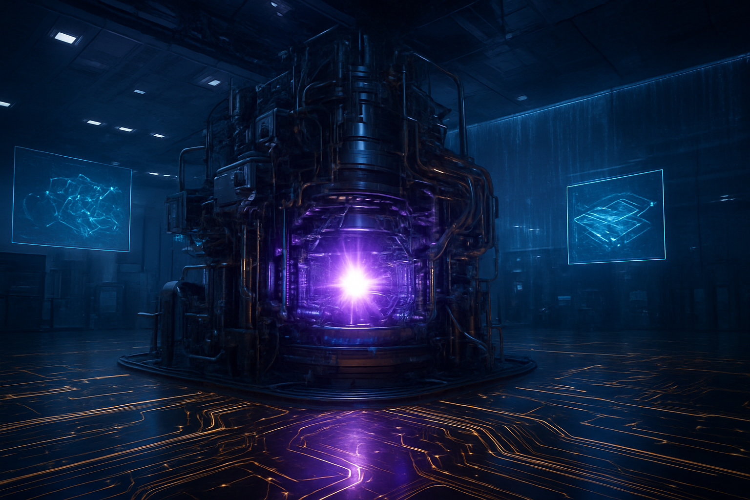
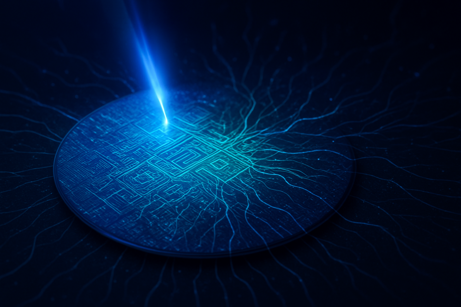
    In a development that has sent shockwaves through the global semiconductor industry, a secretive research collective in Shenzhen has successfully completed and tested a prototype Extreme Ultraviolet (EUV) lithography system. This breakthrough represents the most significant challenge to date against the Western-led blockade on high-end chipmaking equipment. By leveraging a "Chinese Manhattan Project" strategy that combines state-level resources with the expertise of recruited former ASML (NASDAQ: ASML) engineers, China has effectively demonstrated the fundamental physics required to produce sub-7nm chips without Dutch or American equipment.

    The completion of the prototype, which occurred in late 2025, marks a critical pivot in the global "chip war." While the machine is currently an experimental rig rather than a commercial-ready product, its ability to generate the precise 13.5-nanometer wavelength required for advanced lithography suggests that China’s timeline for self-reliance has accelerated. With a stated production target of 2028, the announcement has forced a radical re-evaluation of US-led export controls and the long-term dominance of the current semiconductor supply chain.

    Technical Specifications and the 'Reverse Engineering' Breakthrough

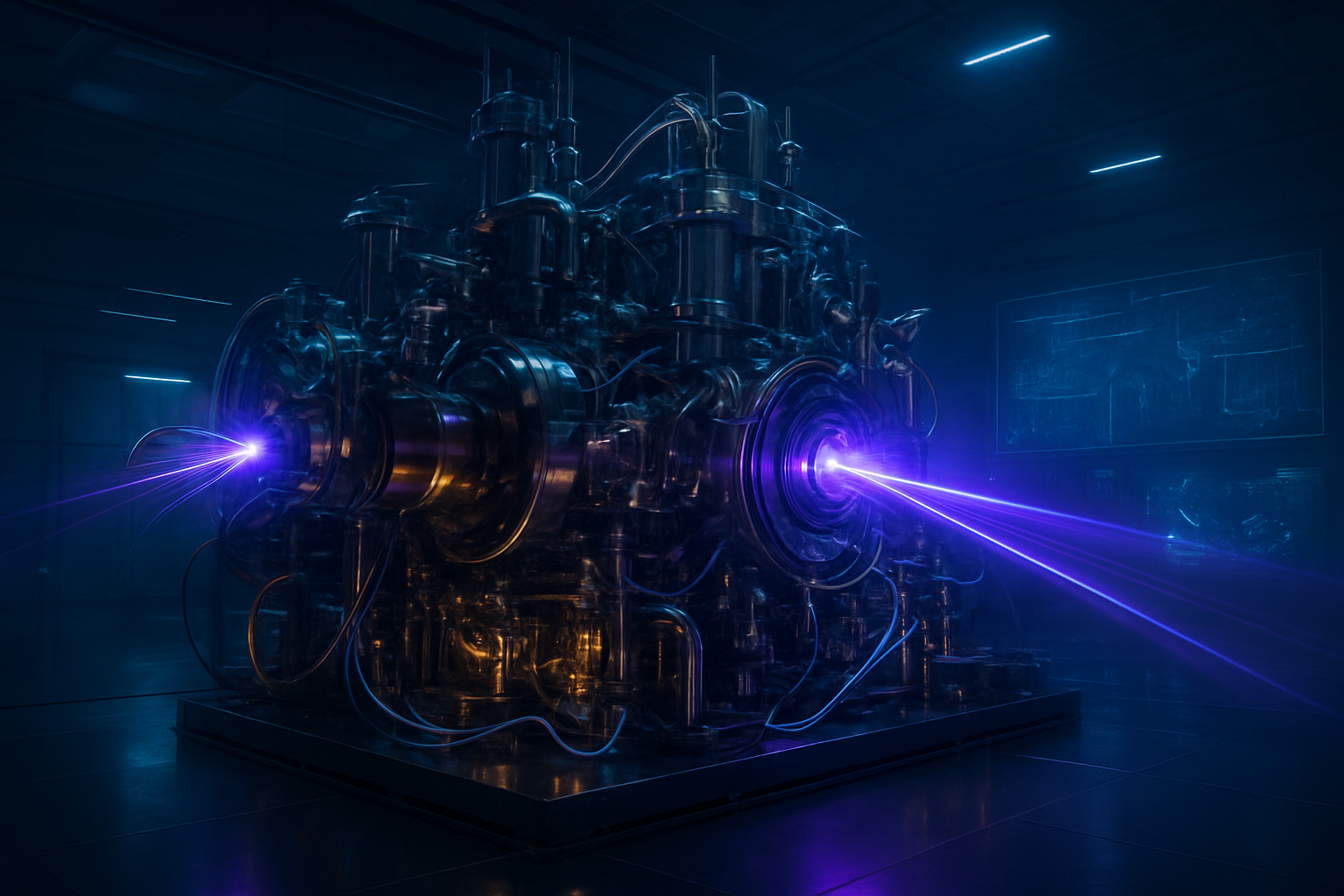
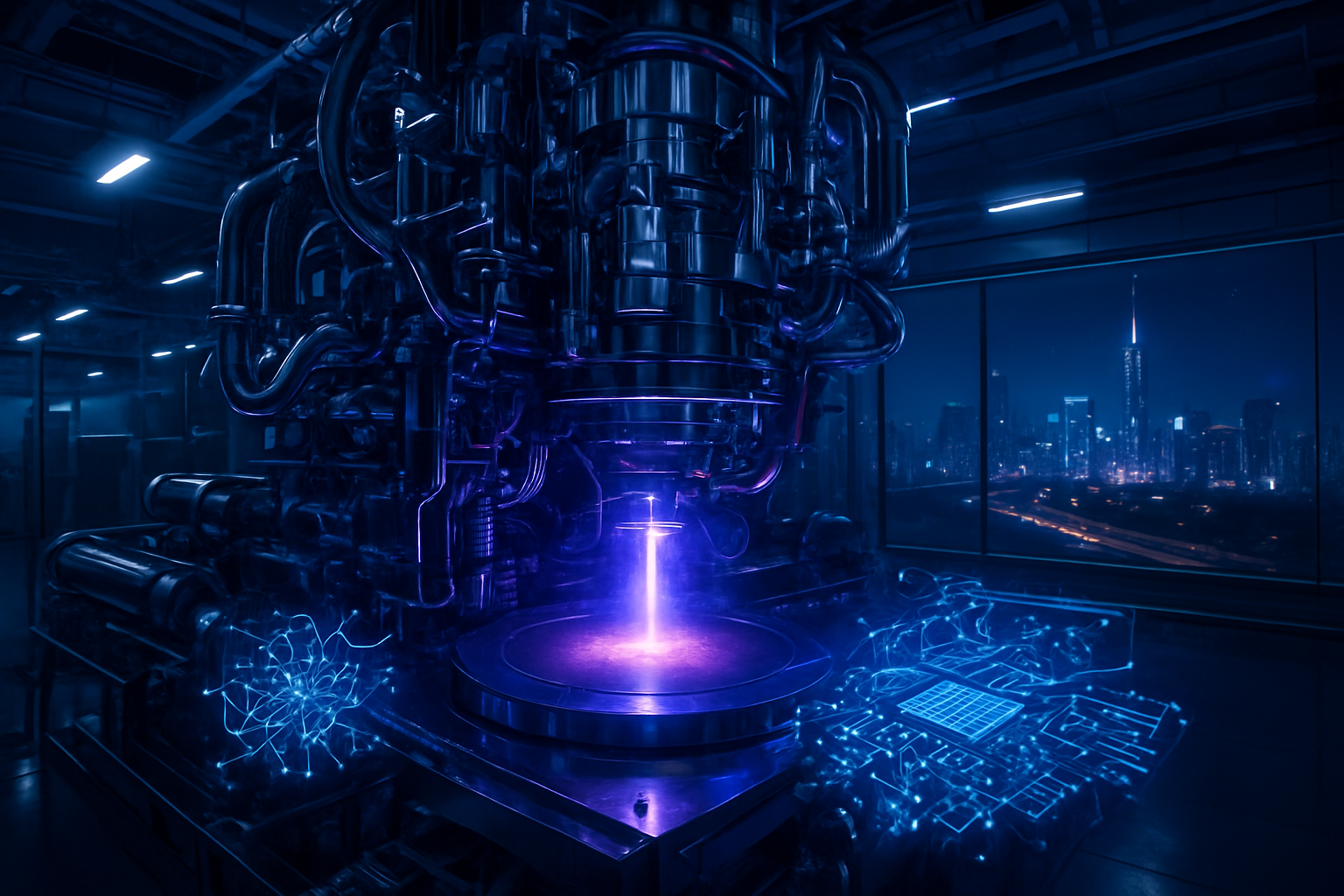
    The Shenzhen prototype is the result of years of clandestine "hybrid engineering," where Chinese researchers and former European industry veterans deconstructed and reimagined the core components of EUV technology. Unlike the Laser-Produced Plasma (LPP) method used by ASML, which relies on high-powered CO2 lasers to hit tin droplets, the Chinese system reportedly utilizes a Laser-Induced Discharge Plasma (LDP) or a solid-state laser-driven source. Initial data suggests the prototype currently produces between 100W and 150W of power. While this is lower than the 250W+ standard required for high-volume manufacturing, it is more than sufficient to prove the viability of the domestic light source and beam delivery system.

    The technical success is largely attributed to a talent-poaching strategy that bypassed international labor restrictions. A team led by figures such as Lin Nan, a former senior researcher at ASML, reportedly utilized dozens of former Dutch and German engineers who worked under aliases within high-security compounds. These experts helped the Chinese Academy of Sciences and Huawei refine the light-source conversion efficiency (CE) to approximately 3.42%, approaching the 5.5% industry benchmark. The prototype itself is massive, reportedly filling nearly an entire factory floor, as it utilizes larger, less integrated components to achieve the necessary precision while domestic miniaturization techniques catch up.

    The most difficult hurdle remains the precision optics. ASML relies on mirrors from Carl Zeiss AG that are accurate to within the width of a single atom. To circumvent the lack of German glass, the Shenzhen team has employed a "distributed aperture" approach, using multiple smaller, domestically produced mirrors and advanced AI-driven alignment algorithms to compensate for surface irregularities. This software-heavy solution to a hardware problem is a hallmark of the new Chinese strategy, differentiating it from the pure hardware-focused precision of Western lithography.

    Market Disruption and the Impact on Global Tech Giants

    The immediate fallout of the Shenzhen prototype has been felt most acutely in the boardrooms of the "Big Three" lithography and chip firms. ASML (NASDAQ: ASML) saw its stock fluctuate as analysts revised 2026 and 2027 revenue forecasts, fearing the eventual loss of the Chinese market—which formerly accounted for nearly 20% of its business. While ASML still maintains a massive lead in High-NA (Numerical Aperture) EUV technology, the realization that China can produce "good enough" EUV for domestic needs threatens the long-term premium on Western equipment.

    For Chinese domestic players, the breakthrough is a catalyst for growth. Companies like Naura Technology Group (SHE: 002371) and Semiconductor Manufacturing International Corporation (HKG: 0981), better known as SMIC, are expected to be the primary beneficiaries of this "Manhattan Project" output. SMIC is reportedly already preparing its fabrication lines for the first integration tests of the Shenzhen prototype’s subsystems. This development also provides a massive strategic advantage to Huawei, which has transitioned from a telecommunications giant to the de facto architect of China’s independent semiconductor ecosystem, coordinating the supply chain for these new lithography machines.

    Conversely, the development poses a complex challenge for American firms like Nvidia (NASDAQ: NVDA) and Intel (NASDAQ: INTC). While they currently benefit from the US-led export restrictions that hamper their Chinese competitors, the emergence of a domestic Chinese EUV capability could eventually lead to a glut of advanced chips in the Asian market, driving down global margins. Furthermore, the success of China’s reverse-engineering efforts suggests that the "moat" around Western IP may be thinner than previously estimated, potentially leading to more aggressive patent litigation in international courts.

    A New Chapter in the Global AI and Silicon Landscape

    The broader significance of this breakthrough cannot be overstated; it represents a fundamental shift in the AI landscape. Advanced AI models, from LLMs to autonomous systems, are entirely dependent on the high-density transistors that only EUV lithography can provide. By cracking the EUV code, China is not just making chips; it is securing the foundational infrastructure required for AI supremacy. This achievement is being compared to the 1964 "596" nuclear test, a moment of national pride that signals China's refusal to be sidelined by international technology regimes.

    However, the "Chinese Manhattan Project" strategy also raises significant concerns regarding intellectual property and the future of global R&D collaboration. The use of former ASML engineers and the reliance on secondary-market components for reverse engineering highlights a widening rift in engineering ethics and international law. Critics argue that this success validates "IP theft as a national strategy," while proponents in Beijing frame it as a necessary response to "technological bullying" by the United States. This divergence ensures that the semiconductor industry will remain the primary theater of geopolitical conflict for the remainder of the decade.

    Compared to previous milestones, such as SMIC’s successful 7nm production using older DUV (Deep Ultraviolet) machines, the EUV prototype is a much higher "wall" to have scaled. DUV multi-patterning was an exercise in optimization; EUV is an exercise in fundamental physics. By mastering the 13.5nm wavelength, China has moved from being a fast-follower to a genuine contender in the most difficult manufacturing process ever devised by humanity.

    The Road to 2028: Challenges and Next Steps

    The path from a laboratory prototype to a production-grade machine is fraught with engineering hurdles. The most pressing challenge for the Shenzhen team is "yield and reliability." A prototype can etch a few circuits in a controlled environment, but a commercial machine must operate 24/7 with 99% uptime and produce millions of chips with minimal defects. Experts predict that the next two years will be focused on "hardening" the system—miniaturizing the power supplies, improving the vacuum chambers, and perfecting the "mask" technology that defines the chip patterns.

    Near-term developments will likely include the deployment of "Alpha" versions of these machines to SMIC’s specialized "black sites" for experimental runs. We can also expect to see China ramp up its domestic production of ultra-pure chemicals and photoresists, the "ink" of the lithography process, which are currently still largely imported from Japan. The 2028 production target is aggressive but, given the progress made since 2023, no longer dismissed as impossible by Western intelligence.

    The ultimate goal is the 2030 milestone of mass-market, entirely "un-Sinoed" (China-independent) advanced chips. If achieved, this would effectively render current US export controls obsolete. Analysts are closely watching for any signs of "Beta" testing in Shenzhen, as well as potential diplomatic or trade retaliations from the Netherlands and the US, which may attempt to tighten restrictions on the sub-components that China still struggles to manufacture domestically.

    Conclusion: A Paradigm Shift in Semiconductor Sovereignty

    The completion of the Shenzhen EUV prototype is a landmark event in the history of technology. It proves that despite the most stringent sanctions in the history of the semiconductor industry, a focused, state-funded effort can overcome immense technical barriers through a combination of talent acquisition, reverse engineering, and sheer national will. The "Chinese Manhattan Project" has moved from a theoretical threat to a functional reality, signaling the end of the Western monopoly on the tools used to build the future.

    As we move into 2026, the key takeaway is that the "chip gap" is closing faster than many anticipated. While China still faces a grueling journey to achieve commercial yields and reliable mass production, the fundamental physics of EUV are now within their grasp. In the coming months, the industry should watch for updates on the Shenzhen team’s optics breakthroughs and any shifts in the global talent market, as the race for the next generation of engineers becomes even more contentious. The silicon curtain has been drawn, and on the other side, a new era of semiconductor competition has begun.


    This content is intended for informational purposes only and represents analysis of current AI developments.

    TokenRing AI delivers enterprise-grade solutions for multi-agent AI workflow orchestration, AI-powered development tools, and seamless remote collaboration platforms.
    For more information, visit https://www.tokenring.ai/.

  • The Silicon Curtain Descends: China Unveils Shenzhen EUV Prototype in ‘Manhattan Project’ Breakthrough

    The Silicon Curtain Descends: China Unveils Shenzhen EUV Prototype in ‘Manhattan Project’ Breakthrough

    As the calendar turns to 2026, the global semiconductor landscape has been fundamentally reshaped by a seismic announcement from Shenzhen. Reports have confirmed that a high-security research facility in China’s technology hub has successfully operated a functional Extreme Ultraviolet (EUV) lithography prototype. Developed under a state-mandated "whole-of-nation" effort often referred to as the "Chinese Manhattan Project," this breakthrough marks the first time a domestic Chinese entity has solved the fundamental physics of EUV light generation—a feat previously thought to be a decade away.

    The emergence of this operational machine, which reportedly utilizes a novel Laser-Induced Discharge Plasma (LDP) light source, signals a direct challenge to the Western monopoly on leading-edge chipmaking. For years, the Dutch firm ASML Holding N.V. (NASDAQ:ASML) has been the sole provider of EUV tools, which are essential for producing chips at 7nm and below. By achieving this milestone, China has effectively punctured the "hard ceiling" of Western export controls, setting an aggressive roadmap to reach 2nm parity by 2028 and threatening to bifurcate the global technology ecosystem into two distinct, non-interoperable stacks.

    Breaking the Light Barrier: The LDP Innovation

    The Shenzhen prototype represents a significant departure from the industry-standard architecture pioneered by ASML. While ASML’s machines rely on Laser-Produced Plasma (LPP)—where high-power $CO_2$ lasers vaporize tin droplets 50,000 times per second—the Chinese system utilizes Laser-Induced Discharge Plasma (LDP). Developed by a consortium led by the Harbin Institute of Technology (HIT) and the Shanghai Institute of Optics and Fine Mechanics (SIOM), the LDP source uses a solid-state laser to vaporize tin, followed by a high-voltage discharge to create the plasma. This approach is technically distinct and avoids many of the specific patents held by Western firms, though it currently requires a much larger physical footprint, with the prototype reportedly filling an entire factory floor.

    Technical specifications leaked from the Shenzhen facility indicate that the machine has achieved a stable 13.5nm EUV beam with a conversion efficiency of 3.42%. While this is still below the 5% to 6% efficiency required for high-volume commercial throughput, it is a massive leap from previous experimental results. The light source is currently outputting between 100W and 150W, with engineers targeting 250W for a production-ready model. The project has been bolstered by a "human intelligence" campaign that successfully recruited dozens of former ASML engineers, including high-ranking specialists like Lin Nan, who reportedly filed multiple EUV patents under an alias at SIOM after leaving the Dutch giant.

    Initial reactions from the semiconductor research community have been a mix of skepticism and alarm. Experts at the Interuniversity Microelectronics Centre (IMEC) note that while the physics of the light source have been validated, the immense challenge of precision optics remains. China’s Changchun Institute of Optics, Fine Mechanics and Physics (CIOMP) is tasked with developing the objective lens assembly and interferometers required to focus that light with sub-nanometer accuracy. Industry insiders suggest that while the machine is not yet ready for mass production, it serves as a "proof of concept" that justifies the billions of dollars in state subsidies poured into the project over the last three years.

    Market Shockwaves and the Rise of the 'Sovereign Stack'

    The confirmation of the Shenzhen prototype has sent shockwaves through the executive suites of Silicon Valley and Hsinchu. Huawei Technologies, the primary coordinator and financier of the project, stands to be the biggest beneficiary. By integrating this domestic EUV tool into its Dongguan testing facilities, Huawei aims to secure a "sovereign supply chain" that is immune to US Department of Commerce sanctions. This development directly benefits Shenzhen-based startups like SiCarrier Technologies, which provides the critical etching and metrology tools needed to complement the EUV system, and SwaySure Technology, a Huawei-linked firm focused on domestic DRAM production.

    For global giants like Intel Corporation (NASDAQ:INTC) and Taiwan Semiconductor Manufacturing Company (NYSE:TSM), the breakthrough accelerates an already frantic arms race. Intel has doubled down on its "first-mover" advantage with ASML’s next-generation High-NA EUV machines, aiming to launch its 1.4nm (14A) node by late 2026 to maintain a technological "moat." Meanwhile, TSMC has reportedly accelerated its A16 and A14 roadmaps, realizing that their "Silicon Shield" now depends on maintaining a permanent two-generation lead rather than a monopoly on the equipment itself. The market positioning of ASML has also been called into question, with its stock experiencing volatility as investors price in the eventual loss of the Chinese market, which previously accounted for a significant portion of its DUV (Deep Ultraviolet) revenue.

    The strategic advantage for China lies in its ability to ignore commercial margins in favor of national security. While an ASML EUV machine costs upwards of $200 million and must be profitable for a commercial fab, the Chinese "Manhattan Project" is state-funded. This allows Chinese fabs to operate at lower yields and higher costs, provided they can produce the 5nm and 3nm chips required for domestic AI accelerators like the Huawei Ascend series. This shift threatens to disrupt the existing service-based revenue models of Western toolmakers, as China moves toward a "100% domestic content" mandate for its internal chip industry.

    Global Reshoring and the 'Silicon Curtain'

    The Shenzhen breakthrough is the most significant milestone in the semiconductor industry since the invention of the transistor, signaling the end of the unified global supply chain. It fits into a broader trend of "Global Reshoring," where national governments are treating chip production as a critical utility rather than a globalized commodity. The US Department of Commerce, led by Under Secretary Howard Lutnick, has responded by moving from "selective restrictions" to "structural containment," recently revoking the "validated end-user" status for foreign-owned fabs in China to prevent the leakage of spare parts into the domestic EUV program.

    This development effectively lowers a "Silicon Curtain" between the East and West. On one side is the Western "High-NA" stack, led by the US, Japan, and the Netherlands, focused on high-efficiency, market-driven, leading-edge nodes. On the other is the Chinese "Sovereign" stack, characterized by state-subsidized resilience and a "good enough" philosophy for domestic AI and military applications. The potential concern for the global economy is the creation of two non-interoperable tech ecosystems, which could lead to redundant R&D costs, incompatible AI standards, and a fragmented market for consumer electronics.

    Comparisons to previous AI milestones, such as the release of GPT-4, are apt; while GPT-4 was a breakthrough in software and data, the Shenzhen EUV prototype is the hardware equivalent. It is the physical foundation upon which China’s future AI ambitions rest. Without domestic EUV, China would eventually be capped at 7nm or 5nm using multi-patterning DUV, which is prohibitively expensive and inefficient. With EUV, the path to 2nm and beyond—the "holy grail" of current semiconductor physics—is finally open to them.

    The Road to 2nm: 2028 and Beyond

    Looking ahead, the next 24 months will be critical for the refinement of the Shenzhen prototype. Near-term developments will likely focus on increasing the power of the LDP light source to 250W and improving the reliability of the vacuum systems. Analysts expect the first "EUV-refined" 5nm chips to roll out of Huawei’s Dongguan facility by late 2026, serving as a pilot run for more complex architectures. The ultimate goal remains 2nm parity by 2028, a target that would bring China within striking distance of the global leading edge.

    However, significant challenges remain. Lithography is only one part of the puzzle; China must also master advanced packaging, photoresist chemistry, and high-purity gases—all of which are currently subject to heavy export controls. Experts predict that China will continue to use "shadow supply chains" and domestic innovation to fill these gaps. We may also see the development of alternative paths, such as Steady-State Micro-Bunching (SSMB) particle accelerators, which Beijing is exploring as a way to provide EUV light to entire clusters of lithography machines at once, potentially leapfrogging the throughput of individual ASML units.

    The most immediate application for these domestic EUV chips will be in AI training and inference. As Nvidia Corporation (NASDAQ:NVDA) faces tightening restrictions on its exports to China, the pressure on Huawei to produce a 5nm or 3nm Ascend chip becomes an existential necessity for the Chinese AI industry. If the Shenzhen prototype can be successfully scaled, it will provide the compute power necessary for China to remain a top-tier player in the global AI race, regardless of Western sanctions.

    A New Era of Technological Sovereignty

    The successful operation of the Shenzhen EUV prototype is a watershed moment that marks the transition from a world of technological interdependence to one of technological sovereignty. The key takeaway is that the "unsolvable" problem of EUV lithography has been solved by a second global power, albeit through a different and more resource-intensive path. This development validates China’s "whole-of-nation" approach to science and technology and suggests that financial and geopolitical barriers can be overcome by concentrated state power and strategic talent acquisition.

    In the context of AI history, this will likely be remembered as the moment the hardware bottleneck was broken for the world’s second-largest economy. The long-term impact will be a more competitive, albeit more divided, global tech landscape. While the West continues to lead in absolute performance through High-NA EUV and 1.4nm nodes, the "performance gap" that sanctions were intended to maintain is narrowing faster than anticipated.

    In the coming weeks and months, watch for official statements from the Chinese Ministry of Industry and Information Technology (MIIT) regarding the commercialization roadmap for the "Famous Mountain" suite of tools. Simultaneously, keep a close eye on the US Department of Commerce for further "choke point" restrictions aimed at the LDP light source components. The era of the unified global chip is over; the era of the sovereign silicon stack has begun.


    This content is intended for informational purposes only and represents analysis of current AI and semiconductor developments as of January 1, 2026.

    TokenRing AI delivers enterprise-grade solutions for multi-agent AI workflow orchestration, AI-powered development tools, and seamless remote collaboration platforms. For more information, visit https://www.tokenring.ai/.

  • China Shatters the Silicon Ceiling: Shenzhen Validates First Domestic EUV Lithography Prototype

    China Shatters the Silicon Ceiling: Shenzhen Validates First Domestic EUV Lithography Prototype

    In a move that fundamentally redraws the map of the global semiconductor industry, Chinese state media and industry reports confirmed on December 17, 2025, that a high-security research facility in Shenzhen has successfully validated a functional prototype of a domestic Extreme Ultraviolet (EUV) lithography machine. This milestone, described by analysts as a "Manhattan Project" moment for Beijing, marks the first time a Chinese-made system has successfully generated a stable 13.5nm EUV beam and integrated it with an optical system capable of wafer exposure.

    The validation of this prototype represents a direct challenge to the Western-led blockade of advanced chipmaking equipment. For years, the denial of EUV tools from ASML Holding N.V. (NASDAQ: ASML) was considered a permanent "hard ceiling" that would prevent China from progressing beyond the 7nm node with commercial efficiency. By proving the viability of a domestic EUV light source and optical assembly, China has signaled that it is no longer a question of if it can produce the world’s most advanced chips, but when it will scale that production to meet the demands of its burgeoning artificial intelligence sector.

    Breaking the 13.5nm Barrier: The Physics of Independence

    The Shenzhen prototype, developed through a "whole-of-nation" effort coordinated by Huawei Technologies and Shenzhen SiCarrier Technologies, deviates significantly from the established architecture used by ASML. While ASML’s industry-standard machines utilize Laser-Produced Plasma (LPP)—where high-power CO2 lasers vaporize tin droplets—the Chinese prototype employs Laser-Induced Discharge Plasma (LDP). Technical insiders report that while LDP currently produces a lower power output, estimated between 100W and 150W compared to ASML’s 250W+ systems, it offers a more stable and cost-effective path for initial domestic integration.

    This technical divergence is a strategic necessity. By utilizing LDP and a massive, factory-floor-sized physical footprint, Chinese engineers have successfully bypassed hundreds of restricted patents and components. The system integrates a light source developed by the Harbin Institute of Technology and high-precision reflective mirrors from the Changchun Institute of Optics (CIOMP). Initial testing has confirmed that the machine can achieve the precision required for single-exposure patterning at the 5nm node, a feat that previously required prohibitively expensive and low-yield multi-patterning techniques using older Deep Ultraviolet (DUV) machines.

    The reaction from the global research community has been one of cautious astonishment. While Western experts note that the prototype is not yet ready for high-volume manufacturing, the successful validation of the "physics package"—the generation and control of the 13.5nm wavelength—proves that China has mastered the most difficult aspect of modern lithography. Industry analysts suggest that the team, which reportedly includes dozens of former ASML engineers and specialists, has effectively compressed a decade of semiconductor R&D into less than four years.

    Shifting the AI Balance: Huawei and the Ascend Roadmap

    The immediate beneficiary of this breakthrough is China’s domestic AI hardware ecosystem, led by Huawei and Semiconductor Manufacturing International Corporation (HKG: 0981), commonly known as SMIC. Prior to this validation, SMIC’s attempt to produce 5nm-class chips using DUV multi-patterning resulted in yields as low as 20%, making the production of high-end AI processors like the Huawei Ascend series economically unsustainable. With the EUV prototype now validated, SMIC is projected to recover yields toward the 60% threshold, drastically lowering the cost of domestic AI silicon.

    This development poses a significant competitive threat to NVIDIA Corporation (NASDAQ: NVDA). Huawei has already utilized the momentum of this breakthrough to announce the Ascend 950 series, scheduled for a Q1 2026 debut. Enabled by the "EUV-refined" manufacturing process, the Ascend 950 is projected to reach performance parity with Nvidia’s H100 in training tasks and offer superior efficiency in inference. By moving away from the "power-hungry" architectures necessitated by DUV constraints, Huawei can now design monolithic, high-density chips that compete directly with the best of Silicon Valley.

    Furthermore, the validation of a domestic EUV path secures the supply chain for Chinese tech giants like Baidu, Inc. (NASDAQ: BIDU) and Alibaba Group Holding Limited (NYSE: BABA), who have been aggressively developing their own large language models (LLMs). With a guaranteed domestic source of high-performance compute, these companies can continue their AI scaling laws without the looming threat of further tightened US export controls on H100 or Blackwell-class GPUs.

    Geopolitical Fallout and the End of the "Hard Ceiling"

    The broader significance of the Shenzhen validation cannot be overstated. It marks the effective end of the "hard ceiling" strategy employed by the US and its allies. For years, the assumption was that China could never replicate the complex supply chain of ASML, which relies on thousands of specialized suppliers across Europe and the US. However, by creating a "shadow supply chain" of over 100,000 domestic parts, Beijing has demonstrated a level of industrial mobilization rarely seen in the 21st century.

    This milestone also highlights a shift in the global AI landscape from "brute-force" clusters to "system-level" efficiency. Until now, China had to compensate for its lagging chip technology by building massive, inefficient clusters of lower-end chips. The move toward EUV allows for a transition to "System-on-Chip" (SoC) designs that are physically smaller and significantly more energy-efficient. This is critical for the deployment of AI at the edge—in autonomous vehicles, robotics, and consumer electronics—where power constraints are as important as raw FLOPS.

    However, the breakthrough also raises concerns about an accelerating "tech decoupling." As China achieves semiconductor independence, the global industry may split into two distinct and incompatible ecosystems. This could lead to a divergence in AI safety standards, hardware architectures, and software frameworks, potentially complicating international cooperation on AI governance and climate goals that require global compute resources.

    The Road to 2nm: What Comes Next?

    Looking ahead, the validation of this prototype is merely the first step in a long-term roadmap. The "Shenzhen Cluster" is now focused on increasing the power output of the LDP light source to 250W, which would allow for the high-speed throughput required for mass commercial production. Experts predict that the first "EUV-refined" chips will begin rolling off SMIC’s production lines in late 2026, with 3nm R&D already underway using a secondary, even more ambitious project involving Steady-State Micro-Bunching (SSMB) particle accelerators.

    The ultimate goal for China is to reach the 2nm frontier by 2028 and achieve full commercial parity with Taiwan Semiconductor Manufacturing Company (NYSE: TSM) by the end of the decade. The challenges remain immense: the reliability of domestic photoresists, the longevity of the reflective mirrors, and the integration of advanced packaging (Chiplets) must all be perfected. Yet, with the validation of the EUV prototype, the most significant theoretical and physical hurdle has been cleared.

    A New Era for Global Silicon

    In summary, the validation of China's first domestic EUV lithography prototype in Shenzhen is a watershed moment for the 2020s. It proves that the technological gap between the West and China is closing faster than many anticipated, driven by massive state investment and a focused "whole-of-nation" strategy. The immediate impact will be felt in the AI sector, where domestic chips like the Huawei Ascend 950 will soon have a viable, high-yield manufacturing path.

    As we move into 2026, the tech industry should watch for the first wafer samples from this new EUV line and the potential for a renewed "chip war" as the US considers even more drastic measures to maintain its lead. For now, the "hard ceiling" has been shattered, and the race for 2nm supremacy has officially become a two-player game.


    This content is intended for informational purposes only and represents analysis of current AI developments.

    TokenRing AI delivers enterprise-grade solutions for multi-agent AI workflow orchestration, AI-powered development tools, and seamless remote collaboration platforms.
    For more information, visit https://www.tokenring.ai/.

  • The Silicon Shield Cracks: China Activates Domestic EUV Prototype in Shenzhen, Aiming for 2nm Sovereignty

    The Silicon Shield Cracks: China Activates Domestic EUV Prototype in Shenzhen, Aiming for 2nm Sovereignty

    In a move that has sent shockwaves through the global semiconductor industry, China has officially activated a functional Extreme Ultraviolet (EUV) lithography prototype at a high-security facility in Shenzhen. The development, confirmed by satellite imagery and internal industry reports in late 2025, represents the most significant challenge to Western chip-making hegemony in decades. By successfully generating the elusive 13.5nm light required for sub-7nm chip production, Beijing has signaled that its "Manhattan Project" for semiconductors is no longer a theoretical ambition but a physical reality.

    The immediate significance of this breakthrough cannot be overstated. For years, the United States and its allies have leveraged export controls to deny China access to EUV machines produced exclusively by ASML (NASDAQ: ASML). The activation of this domestic prototype suggests that China is on the verge of bypassing these "chokepoints," potentially reaching 2nm semiconductor independence by 2028-2030. This achievement threatens to dismantle the "Silicon Shield"—the geopolitical theory that Taiwan’s dominance in advanced chipmaking serves as a deterrent against conflict due to the global economic catastrophe that would follow a disruption of its foundries.

    A "Frankenstein" Approach to 13.5nm Light

    The Shenzhen prototype is not a sleek, commercial-ready unit like the ASML NXE series; rather, it is described by experts as a "hybrid apparatus" or a "Frankenstein" machine. Occupying nearly an entire factory floor, the device was reportedly constructed using a combination of reverse-engineered components from older Deep Ultraviolet (DUV) systems and specialized parts sourced through complex international secondary markets. Despite its massive footprint, the machine has successfully achieved a stable 13.5nm wavelength, the holy grail of modern lithography.

    Technically, the breakthrough hinges on two distinct light-source pathways. The first, a solid-state Laser-Produced Plasma (LPP) system developed by the Shanghai Institute of Optics and Fine Mechanics (SIOM), has reached a conversion efficiency of 3.42%. While this trails ASML's 5.5% industrial standard, it is sufficient for the low-volume production of strategic AI and military components. Simultaneously, a second prototype at a Huawei-linked facility in Dongguan is testing Laser-induced Discharge Plasma (LDP) technology. Developed in collaboration with the Harbin Institute of Technology, this LDP method is reportedly more energy-efficient and cost-effective, though it currently produces lower power output than its LPP counterpart.

    The domestic supply chain has also matured rapidly to support this machine. The Changchun Institute of Optics, Fine Mechanics and Physics (CIOMP) has reportedly delivered the critical alignment interferometers needed to position reflective lenses with nanometer-level precision. Meanwhile, companies like Jiangfeng and MLOptics are providing the specialized mirrors required to bounce EUV light—a task of immense difficulty given that EUV light is absorbed by almost all materials, including air.

    Market Disruption and the Corporate Fallout

    The activation of the Shenzhen prototype has immediate and profound implications for the world's leading tech giants. For ASML (NASDAQ: ASML), the long-term loss of the Chinese market—once its largest growth engine—is now a certainty. While ASML still holds a monopoly on High-NA EUV technology required for the most advanced nodes, the emergence of a viable Chinese alternative for standard EUV threatens its future revenue streams and R&D funding.

    Major foundries like Semiconductor Manufacturing International Corporation, or SMIC (HKG: 0981), are already preparing to integrate these domestic tools into their "Project Dragon" production lines. SMIC has been forced to use expensive multi-patterning techniques on older DUV machines to achieve 7nm and 5nm results; the transition to domestic EUV will allow for single-exposure processing, which dramatically lowers costs and improves chip performance. This poses a direct threat to the market positioning of Taiwan Semiconductor Manufacturing Company, or TSMC (NYSE: TSM), and Samsung Electronics (KRX: 005930), as China moves toward self-sufficiency in the high-end AI chips currently dominated by Nvidia (NASDAQ: NVDA).

    Furthermore, analysts predict that China may use its newfound domestic capacity to initiate a price war in "mature nodes" (28nm and above). By flooding the global market with state-subsidized chips, Beijing could potentially squeeze the margins of Western competitors, forcing them out of the legacy chip market and consolidating China’s control over the broader electronic supply chain.

    Ending the Era of the Silicon Shield

    The broader significance of this breakthrough lies in its impact on global security and the "Silicon Shield" doctrine. For decades, the world’s reliance on TSMC (NYSE: TSM) has served as a powerful deterrent against a cross-strait conflict. If China can produce its own 2nm and 5nm chips domestically, it effectively "immunizes" its military and critical infrastructure from Western sanctions and tech blockades. This shift significantly alters the strategic calculus in the Indo-Pacific, as the economic "mutually assured destruction" of a semiconductor cutoff loses its potency.

    This event also formalizes the "Great Decoupling" of the global technology landscape. We are witnessing the birth of two entirely separate technological ecosystems: a "Western Stack" built on ASML and TSMC hardware, and a "China Stack" powered by Huawei and SMIC. This fragmentation will likely lead to incompatible standards in AI, telecommunications, and high-performance computing, forcing third-party nations to choose between two distinct digital spheres of influence.

    The speed of this development has caught many in the AI research community by surprise. Comparisons are already being drawn to the 1950s "Sputnik moment," as the West realizes that export controls may have inadvertently accelerated China’s drive for innovation by forcing it to build an entirely domestic supply chain from scratch.

    The Road to 2nm: 2028 and Beyond

    Looking ahead, the primary challenge for China is scaling. While a prototype in a high-security facility proves the physics, mass-producing 2nm chips with high yields is a monumental engineering hurdle. Experts predict that 2026 and 2027 will be years of "trial and error," as engineers attempt to move from the current "Frankenstein" machines to more compact, reliable commercial units. The goal of achieving 2nm independence by 2028-2030 is ambitious, but given the "whole-of-nation" resources being poured into the project, it is no longer dismissed as impossible.

    Future applications for these domestic chips are vast. Beyond high-end smartphones and consumer electronics, the primary beneficiaries will be China's domestic AI industry and its military modernization programs. With 2nm capability, China could produce the next generation of AI accelerators, potentially rivaling the performance of Nvidia (NASDAQ: NVDA) chips without needing to import a single transistor.

    However, the path is not without obstacles. The precision required for 2nm lithography is equivalent to hitting a golf ball on the moon with a laser from Earth. China still struggles with the ultra-pure chemicals (photoresists) and the high-end metrology tools needed to verify chip quality at that scale. Addressing these gaps in the "chemical and material" side of the supply chain will be the next major focus for Beijing.

    A New Chapter in the Chip Wars

    The activation of the Shenzhen EUV prototype marks a definitive turning point in the 21st-century tech race. It signifies the end of the era where the West could unilaterally dictate the pace of global technological advancement through the control of a few key machines. As we move into 2026, the focus will shift from whether China can build an EUV machine to how quickly they can scale it.

    The long-term impact of this development will be felt in every sector, from the price of consumer electronics to the balance of power in international relations. The "Silicon Shield" is cracking, and in its place, a new era of semiconductor sovereignty is emerging. In the coming months, keep a close eye on SMIC's (HKG: 0981) yield reports and Huawei's upcoming chip announcements, as these will be the first indicators of how quickly this laboratory breakthrough translates into real-world dominance.


    This content is intended for informational purposes only and represents analysis of current AI developments.

    TokenRing AI delivers enterprise-grade solutions for multi-agent AI workflow orchestration, AI-powered development tools, and seamless remote collaboration platforms.
    For more information, visit https://www.tokenring.ai/.

  • Beijing’s Silicon Sovereignty: Inside China’s ‘Manhattan Project’ to Break the EUV Barrier

    Beijing’s Silicon Sovereignty: Inside China’s ‘Manhattan Project’ to Break the EUV Barrier

    As of late December 2025, the global semiconductor landscape has reached a historic inflection point. Reports emerging from Shenzhen and Beijing confirm that China’s state-led "Manhattan Project" for semiconductor independence has achieved its most critical milestone to date: the successful validation of a domestic Extreme Ultraviolet (EUV) lithography prototype. This breakthrough, occurring just as the year draws to a close, signals a dramatic shift in the "Chip War," suggesting that the technological wall erected by Western export controls is beginning to crumble under the weight of unprecedented state investment and engineering mobilization.

    The significance of this development cannot be overstated. For years, the Dutch firm ASML (NASDAQ: ASML) held a global monopoly on the EUV machines required to manufacture the world’s most advanced AI chips. By successfully generating a stable 13.5nm EUV beam using domestically developed light sources, China has moved from a defensive posture of "survival" to an offensive "insurgency." Backed by the $47.5 billion "Big Fund" Phase 3, this mobilization is not merely a corporate endeavor but a national mission overseen by the highest levels of the Central Science and Technology Commission, aimed at ensuring that China’s AI ambitions are no longer beholden to foreign supply chains.

    The Technical Frontier: SAQP, SSMB, and the Shenzhen Breakthrough

    The technical specifications of the new prototype, validated in a high-security facility in Shenzhen, indicate that China is pursuing a dual-track strategy to bypass existing patents. While the current prototype uses a Laser-Induced Discharge Plasma (LDP) system—developed in part by the Harbin Institute of Technology—to vaporize tin and create EUV light, a more ambitious "leapfrog" project is underway in Xiong'an. This secondary project utilizes Steady-State Micro-Bunching (SSMB), a technique that employs a particle accelerator to generate a high-power, continuous EUV beam. Analysts at SemiAnalysis suggest that if successfully scaled, SSMB could theoretically reach power levels exceeding 1kW, potentially surpassing the throughput of current Western lithography standards.

    Simultaneously, Chinese foundries led by SMIC (SHA: 601238) have mastered a stopgap technique known as Self-Aligned Quadruple Patterning (SAQP). By using existing Deep Ultraviolet (DUV) machines to print multiple overlapping patterns, SMIC has achieved volume production of 5nm-class chips. While this method is more expensive and has lower yields than native EUV lithography, the massive subsidies from the National Integrated Circuit Industry Investment Fund (the "Big Fund") have effectively neutralized the "technology tax." This has allowed Huawei to launch its latest Mate 80 series and Ascend 950 AI processors using domestic 5nm silicon, proving that high-performance compute is possible even under a total blockade of the most advanced tools.

    Initial reactions from the AI research community have been a mix of shock and pragmatic reassessment. Experts who previously predicted China would remain a decade behind the West now acknowledge that the gap has closed to perhaps three to five years. The ability to produce 5nm chips at scale, combined with the successful testing of an EUV light source, suggests that China’s roadmap to 2nm production by 2028 is no longer a propaganda goal, but a credible technical objective. Industry veterans note that the recruitment of thousands of specialized engineers—some reportedly former employees of Western semiconductor firms working under aliases—has been the "secret sauce" in solving the complex precision optics and metrology bottlenecks that define EUV technology.

    Market Disruptions: A Bifurcated Global Ecosystem

    This development has sent ripples through the boardrooms of Silicon Valley and Hsinchu. For NVIDIA (NASDAQ: NVDA), the emergence of a viable domestic Chinese AI stack represents a direct threat to its long-term dominance. Huawei’s Ascend 910C and 950 series are now being mandated for use in over 50% of Chinese state-owned data centers, leading analysts at Morgan Stanley (NYSE: MS) to project that NVIDIA’s China revenue will remain flat or decline even as global demand for AI continues to surge. The "sovereign AI" movement in China is no longer a theoretical risk; it is a market reality that is carving out a massive, self-contained ecosystem.

    Meanwhile, TSMC (NYSE: TSM) is accelerating its pivot toward the United States and Europe to de-risk its exposure to the escalating cross-strait tensions and China’s rising domestic capabilities. While TSMC still maintains a two-node lead with its 2nm production, the loss of market share in the high-volume AI inference segment to SMIC is becoming visible in quarterly earnings. For ASML, the "demand cliff" in China—previously its most profitable region—is forcing a strategic re-evaluation. As Chinese firms like SMEE (Shanghai Micro Electronics Equipment) and Naura Technology Group (SHE: 002371) begin to replace Dutch components in the lithography supply chain, the era of Western equipment manufacturers having unfettered access to the world’s largest chip market appears to be ending.

    Startups in the Chinese AI space are the immediate beneficiaries of this "Manhattan Project." Companies specializing in "More-than-Moore" technologies—such as advanced chiplet packaging and 3D stacking—are receiving unprecedented support. By connecting multiple 7nm or 5nm dies using high-bandwidth interconnects like Huawei’s proprietary UnifiedBus, these startups are producing AI accelerators that rival the performance of Western "monolithic" chips. This shift toward advanced packaging allows China to offset its lag in raw lithography resolution by excelling in system-level integration and compute density.

    Geopolitics and the New AI Landscape

    The wider significance of China’s 2025 breakthroughs lies in the total bifurcation of the global technology landscape. We are witnessing the birth of two entirely separate, incompatible semiconductor ecosystems: one led by the U.S. and its allies (the "Chip 4" alliance), and a vertically integrated, state-driven Chinese stack. This division mirrors the Cold War era but with much higher stakes, as the winner of the "EUV race" will likely dictate the pace of artificial general intelligence (AGI) development. Analysts at Goldman Sachs (NYSE: GS) suggest that China’s progress has effectively neutralized the "total containment" strategy envisioned by 2022-era sanctions.

    However, this progress comes with significant concerns. The environmental and energy costs of China’s SSMB particle accelerator projects are enormous, and the intense pressure on domestic engineers has led to reports of extreme "996" work cultures within the state-backed labs. Furthermore, the lack of transparency in China’s "shadow supply chain" makes it difficult for international regulators to track the proliferation of dual-use AI technologies. There is also the risk of a global supply glut in legacy and mid-range nodes (28nm to 7nm), as China ramps up capacity to dominate the foundational layers of the global electronics industry while it perfects its leading-edge EUV tools.

    Comparatively, this milestone is being viewed as the semiconductor equivalent of the 1957 Sputnik launch. Just as Sputnik forced the West to revolutionize its aerospace and education sectors, China’s EUV prototype is forcing a massive re-industrialization in the U.S. and Europe. The "Chip War" has evolved from a series of trade restrictions into a full-scale industrial mobilization, where the metric of success is no longer just intellectual property, but the physical ability to manufacture at the atomic scale.

    Looking Ahead: The Road to 2nm and Beyond

    In the near term, the industry expects China to focus on refining the yield of its 5nm SAQP process while simultaneously preparing its first-generation EUV machines for pilot production in 2026. The Xiong'an SSMB facility is slated for completion by mid-2026, which could provide a centralized "EUV factory" capable of feeding multiple lithography stations at once. If this centralized light-source model works, it could fundamentally change the economics of chip manufacturing, making EUV production more scalable than the current standalone machine model favored by ASML.

    Long-term challenges remain, particularly in the realm of precision optics. While China has made strides in generating EUV light, the mirrors required to reflect that light with atomic precision—currently a specialty of Germany’s Zeiss—remain a significant bottleneck. Experts predict that the next two years will be a "war of attrition" in material science, as Chinese researchers attempt to replicate or surpass the multilayer coatings required for high-NA (Numerical Aperture) EUV systems. The goal is clear: by 2030, Beijing intends to be the world leader in both AI software and the silicon that powers it.

    Summary and Final Thoughts

    The events of late 2025 mark the end of the "sanctions era" and the beginning of the "parallel era." China’s successful validation of an EUV prototype and the mass production of 5nm chips via DUV-based patterning prove that state-led mobilization can overcome even the most stringent export controls. While the West still holds the lead in the absolute frontier of 2nm and High-NA EUV, the gap is no longer an unbridgeable chasm. The "Manhattan Project" for chips has succeeded in its primary goal: ensuring that China cannot be cut off from the future of AI.

    As we move into 2026, the tech industry should watch for the first "all-domestic" AI server clusters powered by these new chips. The success of the Xiong'an SSMB facility will be the next major bellwether for China’s ability to leapfrog Western technology. For investors and policymakers alike, the takeaway is clear: the global semiconductor monopoly is over, and the race for silicon sovereignty has only just begun. The coming months will likely see further consolidation of the Chinese supply chain and perhaps a new wave of Western policy responses as the reality of a self-sufficient Chinese AI industry sets in.


    This content is intended for informational purposes only and represents analysis of current AI developments.

    TokenRing AI delivers enterprise-grade solutions for multi-agent AI workflow orchestration, AI-powered development tools, and seamless remote collaboration platforms.
    For more information, visit https://www.tokenring.ai/.

  • China’s Secret Lithography Race: Prototyping EUV and Extending DUV Life

    China’s Secret Lithography Race: Prototyping EUV and Extending DUV Life

    In a move that signals a tectonic shift in the global semiconductor landscape, reports from high-security research facilities in Shenzhen and Shanghai indicate that China has successfully prototyped its first Extreme Ultraviolet (EUV) lithography machine. As of late 2024 and throughout 2025, the Chinese government has accelerated its "Manhattan Project" for chips, aiming to bypass stringent Western export controls that have sought to freeze the nation’s logic chip capabilities at the 7-nanometer (nm) threshold. This breakthrough, while still in the laboratory testing phase, represents the first credible domestic challenge to the monopoly held by the Dutch giant ASML (NASDAQ: ASML).

    The significance of this development cannot be overstated. For years, the inability to source EUV machinery—the only technology capable of efficiently printing features smaller than 7nm—was viewed as the "glass ceiling" for Chinese AI and high-performance computing. By successfully generating a stable 13.5nm EUV beam and integrating domestic projection optics, China is signaling to the world that it is no longer content with being a generation behind. While commercial-scale production remains years away, the prototype serves as a definitive proof of concept that the era of Western technological containment may be entering a period of diminishing returns.

    Technical Breakthroughs: LDP, LPP, and the SSMB Leapfrog

    The technical specifications of China’s EUV prototype reveal a multi-track engineering strategy designed to mitigate the risk of component failure. Unlike ASML’s high-NA systems, which rely on Laser Produced Plasma (LPP) powered by massive CO2 lasers, the Chinese prototype led by Huawei and SMEE (Shanghai Micro Electronics Equipment) utilizes a Laser-Induced Discharge Plasma (LDP) source. Developed by the Harbin Institute of Technology, this LDP source reportedly achieved power levels between 100W and 150W in mid-2025. While this is lower than the 250W+ required for high-volume manufacturing, it is sufficient for the "first-light" testing of 5nm-class logic circuits.

    Beyond the LDP source, the most radical technical departure is the Steady-State Micro-Bunching (SSMB) project at Tsinghua University. Rather than a standalone machine, SSMB uses a particle accelerator (synchrotron) to generate a continuous, high-power EUV beam. Construction of a dedicated SSMB-EUV facility began in Xiong’an in early 2025, with theoretical power outputs exceeding 1kW. This "leapfrog" approach differs from existing technology by centralizing the light source for multiple lithography stations, potentially offering a more scalable path to 2nm and 1nm nodes than the pulsed-light methods currently used by the rest of the industry.

    Initial reactions from the AI research community have been a mix of skepticism and alarm. Experts from the Interuniversity Microelectronics Centre (IMEC) note that while a prototype is a milestone, the "yield gap"—the ability to print millions of chips with minimal defects—remains a formidable barrier. However, industry analysts admit that the progress in domestic projection optics, spearheaded by the Changchun Institute of Optics (CIOMP), has surpassed expectations, successfully manufacturing the ultra-smooth reflective mirrors required to steer EUV light without significant energy loss.

    Market Impact: The DUV Longevity Strategy and the Yield War

    While the EUV prototype grabs headlines, the immediate survival of the Chinese chip industry relies on extending the life of older Deep Ultraviolet (DUV) systems. SMIC (HKG: 0981) has pioneered the use of Self-Aligned Quadruple Patterning (SAQP) to push existing DUV immersion tools to their physical limits. By late 2025, SMIC reportedly achieved a pilot run for 5nm AI processors, intended for Huawei’s next-generation Ascend series. This strategy allows China to maintain production of advanced AI silicon despite the Dutch government revoking export licenses for ASML’s Twinscan NXT:1980i units in late 2024.

    The competitive implications are severe for global giants. Companies like TSMC (NYSE: TSM) and Intel (NASDAQ: INTC) now face a competitor that is willing to accept significantly lower yields—estimated at 30-35% for 5nm DUV—to achieve strategic autonomy. This "cost-blind" manufacturing, subsidized by the $47 billion National Integrated Circuit Fund Phase III (Big Fund III), threatens to disrupt the market positioning of Western fabless companies. If China can produce "good enough" AI chips domestically, the addressable market for high-end exports from Nvidia or AMD could shrink faster than anticipated.

    Furthermore, Japanese equipment makers like Nikon (TYO: 7731) and Tokyo Electron (TYO: 8035) are feeling the squeeze. As Japan aligns its export controls with the US, Chinese fabs are rapidly replacing Japanese cleaning and metrology tools with domestic alternatives from startups like Yuliangsheng. This forced decoupling is accelerating the maturation of a parallel Chinese semiconductor supply chain that is entirely insulated from Western sanctions, potentially creating a bifurcated global market where technical standards and equipment ecosystems no longer overlap.

    Wider Significance: The End of Unipolar Tech Supremacy

    The emergence of a Chinese EUV prototype marks a pivotal moment in the broader AI landscape. It suggests that the "moat" created by extreme manufacturing complexity is not impassable. This development mirrors previous milestones, such as the Soviet Union’s rapid development of atomic capabilities or China’s own "Two Bombs, One Satellite" program. It reinforces the trend of "technological sovereignty," where nations view semiconductor manufacturing not just as a business, but as a core pillar of national defense and AI-driven governance.

    However, this race raises significant concerns regarding global stability and the environment. The energy intensity of SSMB-EUV facilities and the chemicals required for SAQP multi-patterning are substantial. Moreover, the lack of transparency in China’s high-security labs makes it difficult for international bodies to monitor for safety or ethical standards in semiconductor manufacturing. The move also risks a permanent split in AI development, with one "Western" stack optimized for EUV efficiency and a "Chinese" stack optimized for DUV-redundancy and massive-scale parallelization.

    Comparisons to the 2023 "Huawei Mate 60 Pro" shock are inevitable. While that event proved China could reach 7nm, the 2025 EUV prototype proves they have a roadmap for what comes next. The geopolitical pressure, rather than stifling innovation, appears to have acted as a catalyst, forcing Chinese firms to solve fundamental physics problems that they previously would have outsourced to ASML or Nikon. This suggests that the era of unipolar tech supremacy is rapidly giving way to a more volatile, multipolar reality.

    Future Outlook: The 2028 Commercial Horizon

    Looking ahead, the next 24 to 36 months will be defined by the transition from lab prototypes to pilot production lines. Experts predict that China will attempt to integrate its LDP light sources into a full-scale "Alpha" lithography tool by 2026. The ultimate goal is a commercial-ready 5nm EUV system by 2028. In the near term, expect to see more "hybrid" manufacturing, where DUV-SAQP is used for most layers of a chip, while the domestic EUV prototype is used sparingly for the most critical, high-density layers.

    The challenges remain immense. Metrology (measuring chip features at the atomic scale) and photoresist chemistry (the light-sensitive liquid used to print patterns) are still major bottlenecks. If China cannot master these supporting technologies, even the most powerful light source will be useless. However, the prediction among industry insiders is that China will continue to "brute force" these problems through massive talent recruitment from the global diaspora and relentless domestic R&D spending.

    Summary and Final Thoughts

    China’s dual-track approach—prototyping the future with EUV while squeezing every last drop of utility out of DUV—is a masterclass in industrial resilience. By late 2025, the narrative has shifted from "Can China survive the sanctions?" to "How quickly can China achieve parity?" The successful prototype of an EUV machine, even in a crude form, is a landmark achievement in AI history, signaling that the most complex machine ever built by humans is no longer the exclusive province of a single Western company.

    In the coming weeks and months, watch for the official unveiling of the SSMB facility in Xiong’an and potential "stealth" chip releases from Huawei that utilize these new manufacturing techniques. The semiconductor war is no longer just about who has the best tools today; it is about who can innovate their way out of a corner. For the global AI industry, the message is clear: the silicon ceiling has been cracked, and the race for 2nm supremacy is now a two-player game.


    This content is intended for informational purposes only and represents analysis of current AI developments.

    TokenRing AI delivers enterprise-grade solutions for multi-agent AI workflow orchestration, AI-powered development tools, and seamless remote collaboration platforms.
    For more information, visit https://www.tokenring.ai/.

  • China Shatters the Silicon Monopoly: Domestic EUV Breakthrough Signals the End of ASML’s Hegemony

    China Shatters the Silicon Monopoly: Domestic EUV Breakthrough Signals the End of ASML’s Hegemony

    In a development that has sent shockwaves through the global semiconductor industry, reports emerging in late 2025 confirm that China has successfully breached the "technological wall" of Extreme Ultraviolet (EUV) lithography. A high-security facility in Shenzhen has reportedly validated a functional domestic EUV prototype, marking the first time a nation has independently replicated the complex light-source technology previously monopolized by the Dutch giant ASML (NASDAQ:ASML). This breakthrough signals a decisive shift in the global "chip war," suggesting that the era of Western-led containment through equipment bottlenecks is rapidly drawing to a close.

    The immediate significance of this achievement cannot be overstated. For years, EUV lithography—the process of using 13.5nm wavelength light to etch microscopic circuits onto silicon—was considered the "Holy Grail" of manufacturing, accessible only to those with access to ASML's multi-billion dollar supply chain. China’s success in developing a working prototype, combined with Semiconductor Manufacturing International Corp (SMIC) (HKG:0981) reaching volume production on its 5nm-class nodes, effectively bypasses the most stringent U.S. export controls. This development ensures that China’s domestic AI and high-performance computing (HPC) sectors will have a sustainable, sovereign path toward the 2nm frontier.

    Breaking the 13.5nm Barrier: The SSMB and LDP Revolution

    Technically, the Chinese breakthrough deviates significantly from the architecture pioneered by ASML. While ASML utilizes Laser-Produced Plasma (LPP)—where high-power CO2 lasers vaporize tin droplets 50,000 times a second—the new Shenzhen prototype reportedly employs Laser-Induced Discharge Plasma (LDP). This method uses a combination of lasers and high-voltage discharge to generate the required plasma, a path that experts suggest is more cost-effective and simpler to maintain, even if it currently operates at a lower power output of approximately 50–100W.

    Parallel to the LDP efforts, a more radical "Manhattan Project" for chips is unfolding in Xiong'an. Led by Tsinghua University, the Steady-State Micro-Bunching (SSMB) project utilizes a particle accelerator to generate a "clean" and continuous EUV beam. Unlike the pulsed light of traditional lithography, SSMB could theoretically reach power levels of 1kW or higher, potentially leapfrogging ASML’s current High-NA EUV capabilities by providing a more stable light source with fewer debris issues. This dual-track approach—LDP for immediate industrial application and SSMB for future-generation dominance—demonstrates a sophisticated R&D strategy that has outpaced Western intelligence estimates.

    Furthermore, Huawei has played a pivotal role as the coordinator of a "shadow supply chain." Recent patent filings reveal that Huawei and its partner SiCarrier have perfected Self-Aligned Quadruple Patterning (SAQP) for 2nm-class features. While this "brute force" method using older Deep Ultraviolet (DUV) tools was once considered economically unviable due to low yields, the integration of domestic EUV prototypes is expected to stabilize production. Initial reactions from the international research community suggest that while China still trails in yield efficiency, the fundamental physics and engineering hurdles have been cleared.

    Market Disruption: ASML’s Demand Cliff and the Rise of the "Two-Track" Supply Chain

    The emergence of a viable Chinese EUV alternative poses an existential threat to the current market structure. ASML (NASDAQ:ASML), which has long enjoyed a 100% market share in EUV equipment, now faces what analysts call a "long-term demand cliff" in China—previously its most profitable region. While ASML’s 2025 revenues remained buoyed by Chinese firms stockpiling DUV spare parts, the projection for 2026 and beyond shows a sharp decline as domestic alternatives from Shanghai Micro Electronics Equipment (SMEE) and SiCarrier begin to replace Dutch and Japanese components in metrology and wafer handling.

    The competitive implications extend to the world’s leading foundries. Taiwan Semiconductor Manufacturing Company (TSMC) (NYSE:TSM) and Intel (NASDAQ:INTC) are now facing a competitor in SMIC that is no longer bound by international sanctions. Although SMIC’s 5nm yields are currently estimated at 33% to 35%—far below TSMC’s ~85%—the massive $47.5 billion "Big Fund" Phase III provides the financial cushion necessary to absorb these costs. For Chinese AI giants like Baidu (NASDAQ:BIDU) and Alibaba (NYSE:BABA), this means a guaranteed supply of domestic chips for their large language models, reducing their reliance on "stripped-down" export-compliant chips from Nvidia (NASDAQ:NVDA).

    Moreover, the strategic advantage is shifting toward "good enough" sovereign technology. Even if Chinese EUV machines are 50% more expensive to operate per wafer, the removal of geopolitical risk is a premium the Chinese government is willing to pay. This is forcing global tech giants to reconsider their manufacturing footprints, as the "Two-Track World"—one supply chain for the West and an entirely separate, vertically integrated one for China—becomes a permanent reality.

    Geopolitical Fallout: The Export Control Paradox

    The success of China’s EUV program highlights the "Export Control Paradox": the very sanctions intended to stall China’s progress served as the ultimate accelerant. By cutting off access to ASML and Lam Research (NASDAQ:LRCX) equipment, the U.S. and its allies forced Chinese firms to collaborate with domestic academia and the military-industrial complex in ways that were previously fragmented. The result is a semiconductor landscape that is more resilient and less dependent on global trade than it was in 2022.

    This development fits into a broader trend of "technological sovereignty" that is defining the mid-2020s. Similar to how the launch of Sputnik galvanized the U.S. space program, the "EUV breakthrough" is being hailed in Beijing as a landmark victory for the socialist market economy. However, it also raises significant concerns regarding global security. A China that is self-sufficient in advanced silicon is a China that is less vulnerable to economic pressure, potentially altering the calculus for regional stability in the Taiwan Strait and the South China Sea.

    Comparisons are already being made to the 1960s nuclear breakthroughs. Just as the world had to adjust to a multi-polar nuclear reality, the semiconductor industry must now adjust to a multi-polar advanced manufacturing reality. The era where a single company in Veldhoven, Netherlands, could act as the gatekeeper for the world’s most advanced AI applications has effectively ended.

    The Road to 2nm: What Lies Ahead

    Looking toward 2026 and 2027, the focus will shift from laboratory prototypes to industrial scaling. The primary challenge for China remains yield optimization. While producing a functional 5nm chip is a feat, producing millions of them at a cost that competes with TSMC is another matter entirely. Experts predict that China will focus on "advanced packaging" and "chiplet" designs to compensate for lower yields, effectively stitching together smaller, functional dies to create massive AI accelerators.

    The next major milestone to watch will be the completion of the SSMB-EUV light source facility in Xiong'an. If this particle accelerator-based approach becomes operational for mass production, it could theoretically allow China to produce 2nm and 1nm chips with higher efficiency than ASML’s current High-NA systems. This would represent a complete leapfrog event, moving China from a follower to a leader in lithography physics.

    However, significant challenges remain. The ultra-precision optics required for EUV—traditionally provided by Carl Zeiss for ASML—are notoriously difficult to manufacture. While the Changchun Institute of Optics has made strides, the durability and coating consistency of domestic mirrors under intense EUV radiation will be the ultimate test of the system's longevity in a 24/7 factory environment.

    Conclusion: A New Era of Global Competition

    The reports of China’s EUV breakthrough mark a definitive turning point in the history of technology. It proves that with sufficient capital, state-level coordination, and a clear strategic mandate, even the most complex industrial monopolies can be challenged. The key takeaways are clear: China has successfully transitioned from "brute-forcing" 7nm chips to developing the fundamental tools for sub-5nm manufacturing, and the global semiconductor supply chain has irrevocably split into two distinct spheres.

    In the history of AI and computing, this moment will likely be remembered as the end of the "unipolar silicon era." The long-term impact will be a more competitive, albeit more fragmented, global market. For the tech industry, the coming months will be defined by a scramble to adapt to this new reality. Investors and policymakers should watch for the first "all-domestic" 5nm chip releases from Huawei in early 2026, which will serve as the ultimate proof of concept for this new era of Chinese semiconductor sovereignty.


    This content is intended for informational purposes only and represents analysis of current AI and semiconductor developments.

    TokenRing AI delivers enterprise-grade solutions for multi-agent AI workflow orchestration, AI-powered development tools, and seamless remote collaboration platforms.
    For more information, visit https://www.tokenring.ai/.

  • China’s “Manhattan Project” Unveils EUV Prototype, Reshaping Global Chip Landscape

    China’s “Manhattan Project” Unveils EUV Prototype, Reshaping Global Chip Landscape

    In a development poised to dramatically reshape the global semiconductor industry, China has reportedly completed a prototype Extreme Ultraviolet (EUV) lithography machine, marking a significant leap in its ambitious "Manhattan Project" to achieve chip sovereignty. This technological breakthrough, confirmed by reports in early 2025, signifies a direct challenge to the long-standing monopoly held by Dutch giant ASML Holding N.V. (AMS: ASML) in the advanced chipmaking arena. The immediate significance of this achievement cannot be overstated: it represents a critical step for Beijing in bypassing stringent US-led export controls and securing an independent supply chain for the cutting-edge semiconductors vital for artificial intelligence, 5G, and advanced military applications.

    The initiative, characterized by its secrecy, state-driven funding, and a "whole-of-nation" approach, underscores China's unwavering commitment to technological self-reliance. While the prototype has successfully generated EUV light—the essential ingredient for advanced chipmaking—it has yet to produce functional chips. Nevertheless, its existence alone signals China's potential to disrupt the delicate balance of power in the tech world, demonstrating a resolve to overcome external dependencies and establish itself as a formidable player at the forefront of semiconductor innovation.

    Technical Prowess and the Road Less Traveled

    The completion of China's prototype EUV lithography machine in early 2025, within a highly secure laboratory in Shenzhen, represents a monumental engineering feat. This colossal apparatus, sprawling across nearly an entire factory floor, is currently undergoing rigorous testing. The core achievement lies in its ability to generate extreme ultraviolet light, a fundamental requirement for etching the minuscule patterns on silicon wafers that form advanced chips. While ASML's commercial EUV systems utilize a Laser Produced Plasma (LPP) light source, reports indicate that Chinese electronics giant Huawei Technologies Co., Ltd. (SHE: 002502) is actively testing an alternative Laser Discharge Induced Plasma (LDP) light source at its Dongguan facility, with trial production of circuits reportedly commencing in the third quarter of 2025. This LDP method is even speculated by some experts to potentially offer greater efficiency than ASML's established LPP technology.

    The development effort has reportedly been bolstered by a team comprising former engineers from ASML, who are believed to have reverse-engineered critical aspects of the Dutch firm's technology. To circumvent export restrictions, China has resourcefuly sourced parts from older ASML machines available on secondary markets, alongside components from Japanese suppliers like Nikon Corp. (TYO: 7731) and Canon Inc. (TYO: 7751). However, a key challenge remains the acquisition of high-precision optical systems, traditionally supplied by specialized firms like Germany's Carl Zeiss AG, a crucial ASML partner. This reliance on alternative sourcing and reverse engineering has resulted in a prototype that is reportedly significantly larger and less refined than ASML's commercial offerings.

    Despite these hurdles, the functionality of the Chinese prototype in generating EUV light marks a critical divergence from previous approaches, which primarily relied on Deep Ultraviolet (DUV) lithography combined with complex multi-patterning techniques to achieve smaller nodes—a method fraught with yield challenges. While ASML CEO Christophe Fouquet stated in April 2025 that China would need "many, many years" to develop such technology, the swift emergence of this prototype suggests a significantly accelerated timeline. China's ambitious target is to produce working chips from its domestic EUV machine by 2028, with 2030 being considered a more realistic timeframe by many industry observers. This indigenous development promises to free Chinese chipmakers from the technological stagnation imposed by international sanctions, offering a pathway to genuinely compete at the leading edge of semiconductor manufacturing.

    Shifting Tides: Competitive Implications for Global Tech Giants

    China's accelerated progress in domestic EUV lithography, spearheaded by Huawei Technologies Co., Ltd. (SHE: 002502) and Semiconductor Manufacturing International Corporation (SMIC) (HKG: 0981), is poised to trigger a significant reordering of the global technology landscape. The most immediate beneficiaries are Chinese semiconductor manufacturers and tech giants. SMIC, for instance, is reportedly on track to finalize its 5nm chip development by the end of 2025, with Huawei planning to leverage this advanced process for its Ascend 910C AI chip. Huawei itself is aggressively scaling its Ascend AI chip production, aiming to double output in 2025 to approximately 600,000 units, with plans to further increase total output to as many as 1.6 million dies in 2026. This domestic capability will provide a reliable, sanction-proof source of high-performance chips for Chinese tech companies like Alibaba Group Holding Ltd. (NYSE: BABA), DeepSeek, Tencent Holdings Ltd. (HKG: 0700), and Baidu, Inc. (NASDAQ: BIDU), ensuring the continuity and expansion of their AI operations and cloud services within China. Furthermore, the availability of advanced domestic chips is expected to foster a more vibrant ecosystem for Chinese AI startups, potentially lowering entry barriers and accelerating indigenous innovation.

    The competitive implications for Western chipmakers are profound. Companies like NVIDIA Corporation (NASDAQ: NVDA), Advanced Micro Devices, Inc. (NASDAQ: AMD), and Intel Corporation (NASDAQ: INTC), which have historically dominated the high-performance chip market, face a long-term threat to their market share within China and potentially beyond. While NVIDIA's newest Grace Blackwell series processors are seeing strong global demand, its dominance in China is demonstrably weakening due to export controls and the rapid ascent of Huawei's Ascend processors. Reports from early 2025 even suggested that some Chinese-designed AI accelerators were processing complex algorithms more efficiently than certain NVIDIA offerings. If China successfully scales its domestic EUV production, it could bypass Western restrictions on cutting-edge nodes (e.g., 5nm, 3nm), directly impacting the revenue streams of these global leaders.

    Global foundries like Taiwan Semiconductor Manufacturing Company Limited (TSMC) (NYSE: TSM) and Samsung Electronics Co., Ltd. (KRX: 005930), currently at the forefront of advanced chip manufacturing with ASML's EUV machines, could also face increased competition from SMIC. While SMIC's 5nm wafer costs are presently estimated to be up to 50% higher than TSMC's, coupled with lower yields due to its reliance on DUV for these nodes, successful domestic EUV implementation could significantly narrow this gap. For ASML Holding N.V. (AMS: ASML), the current undisputed monarch of EUV technology, China's commercialization of LDP-based EUV would directly challenge its monopoly. ASML CEO Christophe Fouquet has acknowledged that "China will not accept to be cut off from technology," highlighting the inevitability of China's pursuit of self-sufficiency. This intense competition is likely to accelerate efforts among global tech companies to diversify supply chains, potentially leading to a "decoupling" of technological ecosystems and the emergence of distinct standards and suppliers in China.

    Strategically, China's domestic EUV breakthrough grants it unparalleled technological autonomy and national security in advanced semiconductor manufacturing, aligning with the core objectives of its "Made in China 2025" initiative. Huawei, at the helm of this national strategy, is actively building a parallel, independent ecosystem for AI infrastructure, demonstrating a commitment to compensating for limited Western EUV access through alternative architectural strategies and massive domestic production scaling. This geopolitical rebalancing underscores that strategic pressure and export controls can, paradoxically, accelerate indigenous innovation. The success of China's EUV project will likely force a re-evaluation of current export control policies by the US and its allies, as the world grapples with the implications of a truly self-reliant Chinese semiconductor industry.

    A New Epoch: Broader Implications for the AI Landscape and Geopolitics

    The emergence of China's prototype EUV lithography machine in late 2025 is more than just a technical achievement; it is a foundational hardware breakthrough that will profoundly influence the broader Artificial Intelligence landscape and global geopolitical dynamics. EUV lithography is the linchpin for manufacturing the high-performance, energy-efficient chips with sub-7nm, 5nm, 3nm, and even sub-2nm nodes that are indispensable for powering modern AI applications—from sophisticated AI accelerators and neural processing units to large language models and advanced AI hardware for data centers, autonomous systems, and military technologies. Without such advanced manufacturing capabilities, the rapid advancements observed in AI development would face insurmountable obstacles. China's domestic EUV effort is thus a cornerstone of its strategy to achieve self-sufficiency in AI, mitigate the impact of U.S. export controls, and accelerate its indigenous AI research and deployment, effectively securing the "compute" power that has become the defining constraint for AI progress.

    The successful development and eventual mass production of China's EUV lithography machine carries multifaceted impacts. Geopolitically and economically, it promises to significantly reduce China's dependence on foreign technology, particularly ASML Holding N.V.'s (AMS: ASML) EUV systems, thereby enhancing its national security and resilience against export restrictions. This breakthrough could fundamentally alter the global technological balance, intensifying the ongoing "tech cold war" and challenging the West's historical monopoly on cutting-edge chipmaking technology. While it poses a potential threat to ASML's market dominance, it could also introduce new competition in the high-end lithography market, leading to shifts in global supply chains. However, the dual-use potential of advanced AI chips—serving both commercial and military applications—raises significant concerns and could further fuel geopolitical tensions regarding military-technological parity. Technologically, domestic access to EUV would enable China to produce its own cutting-edge AI chips, accelerating its progress in AI research, hardware development, and deployment across various sectors, facilitating new AI hardware architectures crucial for optimizing AI workloads, and potentially narrowing the node gap with leading manufacturers to 5nm, 3nm, or even 2nm by 2030.

    Despite the strategic advantages for China, this development also brings forth several concerns. The technical viability and quality of scaling production, ensuring sustained reliability, achieving comparable throughput, and replicating the precision optical systems of ASML's machines remain significant hurdles. Moreover, the reported reverse-engineering of ASML technology raises intellectual property infringement concerns. Geopolitical escalation is another real risk, as China's success could provoke further export controls and trade restrictions from the U.S. and its allies. The energy consumption of EUV lithography, an incredibly power-intensive process, also poses sustainability challenges as China ramps up its chip production. Furthermore, a faster, unrestrained acceleration of AI development in China, potentially without robust international ethical frameworks, could lead to novel ethical dilemmas and risks on a global scale.

    In the broader context of AI milestones, China's prototype EUV machine can be seen as a foundational hardware breakthrough, akin to previous pivotal moments. Just as powerful GPUs from companies like NVIDIA Corporation (NASDAQ: NVDA) provided the computational backbone for the deep learning revolution, EUV lithography acts as the "unseen engine" that enables the complex designs and high transistor densities required for sophisticated AI algorithms. This intense global investment in advanced chip manufacturing and AI infrastructure mirrors the scale of the dot-com boom or the expansion of cloud computing infrastructure. The fierce competition over AI chips and underlying manufacturing technology like EUV reflects a modern-day scramble for vital strategic resources. The U.S.-China AI rivalry, driven by the race for technological supremacy, is frequently compared to the nuclear arms race of the Cold War era. China's rapid progress in EUV lithography, spurred by export controls, exemplifies how strategic pressure can accelerate domestic innovation in critical technologies, a "DeepSeek moment for lithography" that parallels how Chinese AI models have rapidly caught up to and even rivaled leading Western models despite chip restrictions. This monumental effort underscores a profound shift in the global semiconductor and AI landscapes, intensifying geopolitical competition and potentially reshaping supply chains for decades to come.

    The Road Ahead: China's Ambitions and the Future of Advanced Chipmaking

    The journey from a prototype EUV lithography machine to commercially viable, mass-produced advanced chips is fraught with challenges, yet China's trajectory indicates a determined march towards its goals. In the near term, the focus is squarely on transitioning from successful EUV light generation to the production of functional chips. With a prototype already undergoing testing at facilities like Huawei Technologies Co., Ltd.'s (SHE: 002502) Dongguan plant, the critical next steps involve optimizing the entire manufacturing process. Trial production of circuits using these domestic systems reportedly commenced in the second or third quarter of 2025, with ambitious plans for full-scale or mass production slated for 2026. This period will be crucial for refining the Laser-Induced Discharge Plasma (LDP) method, which Chinese institutions like the Harbin Institute of Technology and the Shanghai Institute of Optics and Fine Mechanics are championing as an alternative to ASML Holding N.V.'s (AMS: ASML) Laser-Produced Plasma (LPP) technology. Success in this phase would validate the LDP approach and potentially offer a simpler, more cost-effective, and energy-efficient pathway to EUV.

    Looking further ahead, China aims to produce functional chips from its EUV prototypes by 2028, with 2030 being a more realistic target for achieving significant commercial output. The long-term vision is nothing less than complete self-sufficiency in advanced chip manufacturing. Should China successfully commercialize LDP-based EUV lithography, it would become the only nation outside the Netherlands with such advanced capabilities, fundamentally disrupting the global semiconductor industry. Experts predict that if China can advance to 3nm or even 2nm chip production by 2030, it could emerge as a formidable competitor to established leaders like ASML, Taiwan Semiconductor Manufacturing Company Limited (TSMC) (NYSE: TSM), and Samsung Electronics Co., Ltd. (KRX: 005930). This would unlock the domestic manufacturing of chips smaller than 7 nanometers, crucial for powering advanced Artificial Intelligence (AI) systems, military applications, next-generation smartphones, and high-performance computing, thereby significantly strengthening China's position in these strategic sectors.

    However, the path to commercial viability is riddled with formidable challenges. Technical optimization remains paramount, particularly in boosting the power output of LDP systems, which currently range from 50-100W but require at least 250W for commercial scale. Replicating the extreme precision of Western optical systems, especially those from Carl Zeiss AG, and developing a comprehensive domestic ecosystem for all critical components—including pellicles, masks, and resist materials—are significant bottlenecks. System integration, given the immense complexity of an EUV scanner, also presents considerable engineering hurdles. Beyond the technical, geopolitical and supply chain restrictions continue to loom, with the risk of further export controls on essential materials and components. While China has leveraged parts from older ASML machines obtained from secondary markets, this approach may not be sustainable or scalable for cutting-edge nodes.

    Expert predictions, while acknowledging China's remarkable progress, largely agree that scaling EUV production to commercially competitive levels will take considerable time. While some researchers, including those from TSMC, have optimistically suggested that China's LDP method could "out-compete ASML," most analysts believe that initial production capacity will likely be constrained. The unwavering commitment of the Chinese government, often likened to a "Manhattan Project," coupled with substantial investments and coordinated efforts across various research institutes and companies like Huawei, is a powerful driving force. This integrated approach, encompassing chip design to fabrication equipment, aims to entirely bypass foreign tech restrictions. The rate of China's progress towards self-sufficiency in advanced semiconductors will ultimately be determined by its ability to overcome these technological complexities and market dynamics, rather than solely by the impact of export controls, fundamentally reshaping the global semiconductor landscape in the coming years.

    The Dawn of a New Era: A Comprehensive Wrap-up

    China's "Manhattan Project" to develop a domestic EUV lithography machine has culminated in the successful creation of a working prototype, a monumental achievement that, as of December 2025, signals a pivotal moment in the global technology race. This breakthrough, driven by an unwavering national imperative for chip sovereignty, represents a direct response to stringent U.S.-led export controls and a strategic move to secure an independent supply chain for advanced semiconductors. Key takeaways include the prototype's ability to generate extreme ultraviolet light, its reliance on a combination of reverse engineering from older ASML Holding N.V. (AMS: ASML) machines, and the innovative adoption of Laser-Induced Discharge Plasma (LDP) technology, which some experts believe could offer advantages over ASML's LPP method. Huawei Technologies Co., Ltd. (SHE: 002502) stands at the forefront of this coordinated national effort, aiming to establish an entire domestic AI supply chain. While the prototype has yet to produce functional chips, with targets set for 2028 and a more realistic outlook of 2030, the progress is undeniable.

    This development holds immense significance in the history of Artificial Intelligence. Advanced AI systems, particularly those underpinning large language models and complex neural networks, demand cutting-edge chips with unparalleled processing power and efficiency—chips predominantly manufactured using EUV lithography. China's ability to master this technology and produce advanced chips domestically would dramatically reduce its strategic dependence on foreign suppliers for the foundational hardware of AI. This would not only enable China to accelerate its AI development independently, free from external bottlenecks, but also potentially shift the global balance of power in AI research and application, bolstering Beijing's quest for leadership in AI and military-technological parity.

    The long-term impact of China's EUV lithography project is poised to be profound and transformative. Should China successfully transition from a functional prototype to commercial-scale production of advanced chips by 2030, it would fundamentally redefine global semiconductor supply chains, challenging ASML's near-monopoly and ushering in a more multipolar semiconductor industry. This achievement would represent a major victory in China's "Made in China 2025" and subsequent self-reliance initiatives, significantly reducing its vulnerability to foreign export controls. While accelerating China's AI development, such a breakthrough is also likely to intensify geopolitical tensions, potentially prompting further countermeasures and heightened competition in the tech sphere.

    In the coming weeks and months, the world will be closely watching for several critical indicators. The most immediate milestone is the prototype's transition from generating EUV light to successfully producing working semiconductor chips, with performance metrics such as resolution capabilities, throughput stability, and yield rates being crucial. Further advancements in LDP technology, particularly in efficiency and power output, will demonstrate China's capacity for innovation beyond reverse-engineering. The specifics of China's 15th five-year plan (2026-2030), expected to be fully detailed next year, will reveal the continued scale of investment and strategic focus on semiconductor and AI self-reliance. Finally, any new export controls or diplomatic discussions from the U.S. and its allies in response to China's demonstrated progress will be closely scrutinized, as the global tech landscape continues to navigate this new era of intensified competition and technological independence.


    This content is intended for informational purposes only and represents analysis of current AI developments.

    TokenRing AI delivers enterprise-grade solutions for multi-agent AI workflow orchestration, AI-powered development tools, and seamless remote collaboration platforms.
    For more information, visit https://www.tokenring.ai/.

  • Unlocking AI’s Full Potential: ASML’s EUV Lithography Becomes the Indispensable Foundation for Next-Gen Chips

    Unlocking AI’s Full Potential: ASML’s EUV Lithography Becomes the Indispensable Foundation for Next-Gen Chips

    The exponential growth of Artificial Intelligence (AI) and its insatiable demand for processing power have rendered traditional chip manufacturing methods inadequate, thrusting ASML's (AMS: ASML) Extreme Ultraviolet (EUV) lithography technology into an immediately critical and indispensable role. This groundbreaking technology, in which ASML holds a global monopoly, uses ultra-short 13.5-nanometer wavelengths of light to etch incredibly intricate patterns onto silicon wafers, enabling the creation of microchips with billions of smaller, more densely packed transistors.

    This unparalleled precision is the bedrock upon which next-generation AI accelerators, data center GPUs, and sophisticated edge AI solutions are built, providing the enhanced processing capabilities and vital energy efficiency required to power the most advanced AI applications today and in the immediate future. Without ASML's EUV systems, the semiconductor industry would face a significant barrier to scaling chip performance, making the continued advancement and real-world deployment of cutting-edge AI heavily reliant on this singular technological marvel.

    The Microscopic Marvel: Technical Deep Dive into EUV's Edge

    ASML's Extreme Ultraviolet (EUV) lithography technology represents a monumental leap in semiconductor manufacturing, enabling the creation of microchips with unprecedented density and performance. This intricate process is crucial for sustaining Moore's Law and powering the latest advancements in artificial intelligence (AI), high-performance computing, and other cutting-edge technologies. ASML is currently the sole supplier of EUV lithography systems globally.

    At the core of ASML's EUV technology is the use of light with an extremely short wavelength of 13.5 nanometers (nm), which is nearly in the X-ray range and more than 14 times shorter than the 193 nm wavelength used in previous Deep Ultraviolet (DUV) systems. This ultra-short wavelength is fundamental to achieving finer resolution and printing smaller features on silicon wafers. Key technical specifications include EUV light generated by firing two separate CO2 laser pulses at microscopic droplets of molten tin 50,000 times per second. Unlike DUV systems that use refractive lenses, EUV light is absorbed by nearly all materials, necessitating operation in a vacuum chamber and the use of highly specialized multi-layer mirrors, developed in collaboration with companies like Carl Zeiss SMT, to guide and focus the light. These mirrors are so precise that if scaled to the size of a country, the largest imperfection would be only about 1 millimeter.

    Current generation NXE systems (e.g., NXE:3400C, NXE:3600D) have a numerical aperture of 0.33, enabling them to print features with a resolution of 13 nm, supporting volume production for 7 nm, 5 nm, and 3 nm logic nodes. The next-generation platform, High-NA EUV (EXE platform, e.g., TWINSCAN EXE:5000, EXE:5200B), significantly increases the numerical aperture to 0.55, improving resolution to just 8 nm. This allows for transistors that are 1.7 times smaller and transistor densities 2.9 times higher. The first High-NA EUV system was delivered in December 2023, with high-volume manufacturing expected between 2025 and 2026 for advanced nodes starting at 2 nm logic. High-NA EUV systems are designed for higher productivity, with initial capabilities of printing over 185 wafers per hour (wph).

    The transition from Deep Ultraviolet (DUV) to Extreme Ultraviolet (EUV) lithography marks a fundamental shift. The most significant difference is the light wavelength—13.5 nm for EUV compared to 193 nm for DUV. DUV systems use refractive lenses and can operate in air, while EUV necessitates an entirely reflective optical system within a vacuum. EUV can achieve much smaller feature sizes, enabling advanced nodes where DUV lithography typically hits its limit around 40-20 nm without complex resolution enhancement techniques like multi-patterning, which EUV often simplifies into a single pass. The AI research community and industry experts have expressed overwhelmingly positive reactions, recognizing EUV's indispensable role in sustaining Moore's Law and enabling the fabrication of the ever-smaller, more powerful, and energy-efficient chips required for the exponential growth in AI, quantum computing, and other advanced technologies.

    Reshaping the AI Battleground: Corporate Beneficiaries and Competitive Edge

    ASML's EUV lithography technology is a pivotal enabler for the advancement of artificial intelligence, profoundly impacting AI companies, tech giants, and startups by shaping the capabilities, costs, and competitive landscape of advanced chip manufacturing. It is critical for producing the advanced semiconductors that power AI systems, allowing for higher transistor densities, increased processing capabilities, and lower power consumption in AI chips. This is essential for scaling semiconductor devices to 7nm, 5nm, 3nm, and even sub-2nm nodes, which are vital for developing specialized AI accelerators and neural processing units.

    The companies that design and manufacture the most advanced AI chips are the primary beneficiaries of ASML's EUV technology. TSMC (NYSE: TSM), as the world's largest contract chipmaker, is a leading implementer of EUV, extensively integrating it into its fabrication processes for nodes such as N7+, N5, N3, and the upcoming N2. TSMC received its first High-NA (High Numerical Aperture) EUV machine in September 2024, signaling its commitment to maintaining leadership in advanced AI chip manufacturing, with plans to integrate it into its A14 (1.4nm) process node by 2027. Samsung Electronics (KRX: 005930) is another key player heavily investing in EUV, planning to deploy High-NA EUV at its 2nm node, potentially ahead of TSMC's 1.4nm timeline, with a significant investment in two of ASML’s EXE:5200B High-NA EUV tools. Intel (NASDAQ: INTC) is actively adopting ASML's EUV and High-NA EUV machines as part of its strategy to regain leadership in chip manufacturing, particularly for AI, with its roadmap including High-NA EUV for its Intel 18A process, with product proof points in 2025. Fabless giants like NVIDIA (NASDAQ: NVDA) and AMD (NASDAQ: AMD) rely entirely on these advanced foundries. ASML's EUV technology is indispensable for producing the highly complex and dense chips that power NVIDIA's AI accelerators, such as the Blackwell architecture and the upcoming 'Rubin' platform, and AMD's high-performance CPUs and GPUs for AI workloads.

    ASML's EUV technology creates a clear divide in the competitive landscape. Tech giants and major AI labs that partner with or own foundries capable of leveraging EUV gain a significant strategic advantage, accessing the most advanced, powerful, and energy-efficient chips crucial for developing and deploying cutting-edge AI models. Conversely, companies without access to EUV-fabricated chips face substantial hurdles, as the computational demands of advanced AI would become "prohibitively expensive or technically unfeasible." ASML's near-monopoly makes it an indispensable "linchpin" and "gatekeeper" of the AI revolution, granting it significant pricing power and strategic importance. The immense capital expenditure (EUV machines cost hundreds of millions of dollars) and the complexity of integrating EUV technology create high barriers to entry for new players and smaller startups in advanced chip manufacturing, concentrating leading-edge AI chip production among a few well-established tech giants.

    The Unseen Engine: Broader Implications for AI and Beyond

    ASML's Extreme Ultraviolet (EUV) lithography technology stands as a pivotal advancement in semiconductor manufacturing, profoundly shaping the landscape of artificial intelligence (AI). By enabling the creation of smaller, more powerful, and energy-efficient chips, EUV is not merely an incremental improvement but a foundational technology indispensable for the continued progression of AI capabilities.

    The relentless demand for computational power in AI, driven by the increasing complexity of algorithms and the processing of vast datasets, necessitates increasingly sophisticated semiconductor hardware. EUV lithography, operating at an ultra-short wavelength of 13.5 nanometers, allows manufacturers to etch incredibly fine features onto silicon wafers, crucial for producing advanced semiconductor nodes like 7nm, 5nm, 3nm, and the forthcoming sub-2nm generations that power cutting-edge AI processors. Without EUV, the semiconductor industry would face significant challenges in meeting the escalating hardware demands of AI, potentially slowing the pace of innovation.

    EUV lithography has been instrumental in extending the viability of Moore's Law, providing the necessary foundation for continued miniaturization and performance enhancement beyond the limits of traditional methods. By enabling the packing of billions of tiny transistors, EUV contributes to significant improvements in power efficiency. This allows AI chips to process more parameters with lower power requirements per computation, reducing the overall energy consumption of AI systems at scale—a crucial benefit as AI applications demand massive computational power. The higher transistor density and performance directly translate into more powerful and capable AI systems, essential for complex AI algorithms, training large language models, and real-time inference at the edge, fostering breakthroughs in areas such as autonomous driving, medical diagnostics, and augmented reality.

    Despite its critical role, ASML's EUV technology faces several significant concerns. Each EUV system is incredibly expensive, costing between $150 million and $400 million, with the latest High-NA models exceeding $370 million, limiting accessibility to a handful of leading chip manufacturers. The machines are marvels of engineering but are immensely complex, comprising over 100,000 parts and requiring operation in a vacuum, leading to high installation, maintenance, and operational costs. ASML's near-monopoly places it at the center of global geopolitical tensions, particularly between the United States and China, with export controls highlighting its strategic importance and impacting sales. This concentration in the supply chain also creates a significant risk, as disruptions can impact advanced chip production schedules globally.

    The impact of ASML's EUV lithography on AI is analogous to several foundational breakthroughs that propelled computing and, subsequently, AI forward. Just as the invention of the transistor revolutionized electronics, EUV pushes the physical limits of transistor density. Similarly, its role in enabling the creation of advanced chips that house powerful GPUs for parallel processing mirrors the significance of the GPU's development for AI. While EUV is not an AI algorithm or a software breakthrough, it is a crucial hardware innovation that unlocks the potential for these software advancements, effectively serving as the "unseen engine" behind the AI revolution.

    The Road Ahead: Future Horizons for EUV and AI

    ASML's Extreme Ultraviolet (EUV) lithography technology is a cornerstone of advanced semiconductor manufacturing, indispensable for producing the high-performance chips that power artificial intelligence (AI) applications. The company is actively pursuing both near-term and long-term developments to push the boundaries of chip scaling, while navigating significant technical and geopolitical challenges.

    ASML's immediate focus is on the rollout of its next-generation High-NA EUV lithography systems, specifically the TWINSCAN EXE:5000 and EXE:5200 platforms. These High-NA systems increase the numerical aperture from 0.33 to 0.55, allowing for a critical dimension (CD) of 8 nm, enabling chipmakers to print transistors 1.7 times smaller and achieve transistor densities 2.9 times higher. The first modules of the EXE:5000 were shipped to Intel (NASDAQ: INTC) in December 2023 for R&D, with high-volume manufacturing using High-NA EUV anticipated to begin in 2025-2026. High-NA EUV is crucial for enabling the production of sub-2nm logic nodes, including 1.5nm and 1.4nm. Beyond High-NA, ASML is in early R&D for "Hyper-NA" EUV technology, envisioned with an even higher numerical aperture of 0.75, expected to be deployed around 2030-2035 to push transistor densities beyond the projected limits of High-NA.

    ASML's advanced EUV lithography is fundamental to the progression of AI hardware, enabling the manufacturing of high-performance AI chips, neural processors, and specialized AI accelerators that demand massive computational power and energy efficiency. By enabling smaller, more densely packed transistors, EUV facilitates increased processing capabilities and lower power consumption, critical for AI hardware across diverse applications, including data centers, edge AI in smartphones, and autonomous systems. High-NA EUV will also support advanced packaging technologies, such as chiplets and 3D stacking, increasingly important for managing the complexity of AI chips and facilitating real-time AI processing at the edge.

    Despite its critical role, EUV technology faces several significant challenges. The high cost of High-NA machines (between €350 million and $380 million per unit) can hinder widespread adoption. Technical complexities include inefficient light sources, defectivity issues (like pellicle readiness), challenges with resist materials at small feature sizes, and the difficulty of achieving sub-2nm overlay accuracy. Supply chain and geopolitical risks, such as ASML's monopoly and export restrictions, also pose significant hurdles. Industry experts and ASML itself are highly optimistic, forecasting significant growth driven by the surging demand for advanced AI chips. High-NA EUV is widely regarded as the "only path to next-generation chips" and an "indispensable" technology for producing powerful processors for data centers and AI, with predictions of ASML achieving a trillion-dollar valuation by 2034-2036.

    The Unseen Architect of AI's Future: A Concluding Perspective

    ASML's Extreme Ultraviolet (EUV) lithography technology stands as a critical enabler in the ongoing revolution of Artificial Intelligence (AI) chips, underpinning advancements that drive both the performance and efficiency of modern computing. The Dutch company (AMS: ASML) holds a near-monopoly in the production of these highly sophisticated machines, making it an indispensable player in the global semiconductor industry.

    Key takeaways highlight EUV's vitality for manufacturing the most advanced AI chips, enabling intricate patterns at scales of 5 nanometers and below, extending to 3nm and even sub-2nm with next-generation High-NA EUV systems. This precision allows for significantly higher transistor density, directly translating to increased processing capabilities and improved energy efficiency—both critical for powerful AI applications. Leading chip manufacturers like Taiwan Semiconductor Manufacturing Co. (NYSE: TSM), Samsung (KRX: 005930), and Intel (NASDAQ: INTC) rely on ASML's EUV machines to produce cutting-edge chips that power everything from NVIDIA's (NASDAQ: NVDA) AI accelerators to Apple's (NASDAQ: AAPL) smartphones. ASML's dominant market position, coupled with robust demand for AI chips, is a significant driver for its projected growth, with the company forecasting annual revenues between €44 billion and €60 billion by 2030.

    The development and widespread adoption of ASML's EUV lithography mark a pivotal moment in AI history. Without this technology, the production of next-generation AI chipsets capable of meeting the ever-growing demands of AI applications would be challenging, potentially stalling the rapid progress seen in the field. EUV is a cornerstone for the future of AI, enabling the complex designs and high transistor densities required for sophisticated AI algorithms, large language models, and real-time processing in areas like self-driving cars, medical diagnostics, and edge AI. It is not merely an advancement but an essential foundation upon which the future of AI and computing is being built.

    The long-term impact of ASML's EUV technology on AI is profound and enduring. By enabling the continuous scaling of semiconductors, ASML ensures that the hardware infrastructure can keep pace with the rapidly evolving demands of AI software and algorithms. This technological imperative extends beyond AI, influencing advancements in 5G, the Internet of Things (IoT), and quantum computing. ASML's role solidifies its position as a "tollbooth" for the AI highway, as it provides the fundamental tools that every advanced chipmaker needs. This unique competitive moat, reinforced by continuous innovation like High-NA EUV, suggests that ASML will remain a central force in shaping the technological landscape for decades to come, ensuring the continued evolution of AI-driven innovations.

    In the coming weeks and months, several key areas will be crucial to monitor. Watch for the successful deployment and performance validation of ASML's next-generation High-NA EUV machines, which are essential for producing sub-2nm chips. The ongoing impact of geopolitical landscape and export controls on ASML's sales to China will also be a significant factor. Furthermore, keep an eye on ASML's order bookings and revenue reports for insights into the balance between robust AI-driven demand and potential slowdowns in other chip markets, as well as any emerging competition or alternative miniaturization technologies, though no immediate threats to ASML's EUV dominance exist. Finally, ASML's progress towards its ambitious gross margin targets of 56-60% by 2030 will indicate the efficiency gains from High-NA EUV and overall cost control. By closely monitoring these developments, observers can gain a clearer understanding of the evolving synergy between ASML's groundbreaking lithography technology and the accelerating advancements in AI.


    This content is intended for informational purposes only and represents analysis of current AI developments.

    TokenRing AI delivers enterprise-grade solutions for multi-agent AI workflow orchestration, AI-powered development tools, and seamless remote collaboration platforms.
    For more information, visit https://www.tokenring.ai/.

  • The Atomic Edge: How Next-Gen Semiconductor Tech is Fueling the AI Revolution

    The Atomic Edge: How Next-Gen Semiconductor Tech is Fueling the AI Revolution

    In a relentless pursuit of computational supremacy, the semiconductor industry is undergoing a transformative period, driven by the insatiable demands of artificial intelligence. Breakthroughs in manufacturing processes and materials are not merely incremental improvements but foundational shifts, enabling chips that are exponentially faster, more efficient, and more powerful. From the intricate architectures of Gate-All-Around (GAA) transistors to the microscopic precision of High-Numerical Aperture (High-NA) EUV lithography and the ingenious integration of advanced packaging, these innovations are reshaping the very fabric of digital intelligence.

    These advancements, unfolding rapidly towards December 2025, are critical for sustaining the exponential growth of AI, particularly in the realm of large language models (LLMs) and complex neural networks. They promise to unlock unprecedented capabilities, allowing AI to tackle problems previously deemed intractable, while simultaneously addressing the burgeoning energy consumption concerns of a data-hungry world. The immediate significance lies in the ability to pack more intelligence into smaller, cooler packages, making AI ubiquitous from hyperscale data centers to the smallest edge devices.

    The Microscopic Marvels: A Deep Dive into Semiconductor Innovation

    The current wave of semiconductor innovation is characterized by several key technical advancements that are pushing the boundaries of physics and engineering. These include a new transistor architecture, a leap in lithography precision, and revolutionary chip integration methods.

    Gate-All-Around (GAA) Transistors (GAAFETs) represent the next frontier in transistor design, succeeding the long-dominant FinFETs. Unlike FinFETs, where the gate wraps around three sides of a vertical silicon fin, GAAFETs employ stacked horizontal "nanosheets" where the gate completely encircles the channel on all four sides. This provides superior electrostatic control over the current flow, drastically reducing leakage current (power wasted when the transistor is off) and improving drive current (power delivered when on). This enhanced control allows for greater transistor density, higher performance, and significantly reduced power consumption, crucial for power-intensive AI workloads. Manufacturers can also vary the width and number of these nanosheets, offering unprecedented design flexibility to optimize for specific performance or power targets. Samsung (KRX: 005930) was an early adopter, integrating GAA into its 3nm process in 2022, with Intel (NASDAQ: INTC) planning its "RibbonFET" GAA for its 20A node (equivalent to 2nm) in 2024-2025, and TSMC (NYSE: TSM) targeting GAA for its N2 process in 2025-2026. The industry universally views GAAFETs as indispensable for scaling beyond 3nm.

    High-Numerical Aperture (High-NA) EUV Lithography is another monumental step forward in patterning technology. Extreme Ultraviolet (EUV) lithography, operating at a 13.5-nanometer wavelength, is already essential for current advanced nodes. High-NA EUV elevates this by increasing the numerical aperture from 0.33 to 0.55. This enhancement significantly boosts resolution, allowing for the patterning of features with pitches as small as 8nm in a single exposure, compared to approximately 13nm for standard EUV. This capability is vital for producing chips at sub-2nm nodes (like Intel's 18A), where standard EUV would necessitate complex and costly multi-patterning techniques. High-NA EUV simplifies manufacturing, reduces cycle times, and improves yield. ASML (AMS: ASML), the sole manufacturer of these highly complex machines, delivered the first High-NA EUV system to Intel in late 2023, with volume manufacturing expected around 2026-2027. Experts agree that High-NA EUV is critical for sustaining the pace of miniaturization and meeting the ever-growing computational demands of AI.

    Advanced Packaging Technologies, including 2.5D, 3D integration, and hybrid bonding, are fundamentally altering how chips are assembled, moving beyond the limitations of monolithic die design. 2.5D integration places multiple active dies (e.g., CPU, GPU, High Bandwidth Memory – HBM) side-by-side on a silicon interposer, which provides high-density, high-speed connections. TSMC's CoWoS (Chip-on-Wafer-on-Substrate) and Intel's EMIB (Embedded Multi-die Interconnect Bridge) are prime examples, enabling incredible bandwidths for AI accelerators. 3D integration involves vertically stacking active dies and interconnecting them with Through-Silicon Vias (TSVs), creating extremely short, power-efficient communication paths. HBM memory stacks are a prominent application. The cutting-edge Hybrid Bonding technique directly connects copper pads on two wafers or dies at ultra-fine pitches (below 10 micrometers, potentially 1-2 micrometers), eliminating solder bumps for even denser, higher-performance interconnects. These methods enable chiplet architectures, allowing designers to combine specialized components (e.g., compute cores, AI accelerators, memory controllers) fabricated on different process nodes into a single, cohesive system. This approach improves yield, allows for greater customization, and bypasses the physical limits of monolithic die sizes. The AI research community views advanced packaging as the "new Moore's Law," crucial for addressing memory bandwidth bottlenecks and achieving the compute density required by modern AI.

    Reshaping the Corporate Battleground: Impact on Tech Giants and Startups

    These semiconductor innovations are creating a new competitive dynamic, offering strategic advantages to some and posing challenges for others across the AI and tech landscape.

    Semiconductor manufacturing giants like TSMC (NYSE: TSM) and Intel (NASDAQ: INTC) are at the forefront of these advancements. TSMC, as the leading pure-play foundry, is critical for most fabless AI chip companies, leveraging its CoWoS advanced packaging and rapidly adopting GAAFETs and High-NA EUV. Its ability to deliver cutting-edge process nodes and packaging provides a strategic advantage to its diverse customer base, including NVIDIA (NASDAQ: NVDA) and Apple (NASDAQ: AAPL). Intel, through its revitalized foundry services and aggressive adoption of RibbonFET (GAA) and High-NA EUV, aims to regain market share, positioning itself to produce AI fabric chips for major cloud providers like Amazon Web Services (AWS). Samsung (KRX: 005930) also remains a key player, having already implemented GAAFETs in its 3nm process.

    For AI chip designers, the implications are profound. NVIDIA (NASDAQ: NVDA), the dominant force in AI GPUs, benefits immensely from these foundry advancements, which enable denser, more powerful GPUs (like its Hopper and upcoming Blackwell series) that heavily utilize advanced packaging for high-bandwidth memory. Its strategic advantage is further cemented by its CUDA software ecosystem. AMD (NASDAQ: AMD) is a strong challenger, leveraging chiplet technology extensively in its EPYC processors and Instinct MI series AI accelerators. AMD's modular approach, combined with strategic partnerships, positions it to compete effectively on performance and cost.

    Tech giants like Google (NASDAQ: GOOGL), Microsoft (NASDAQ: MSFT), and Amazon (NASDAQ: AMZN) are increasingly pursuing vertical integration by designing their own custom AI silicon (e.g., Google's TPUs, Microsoft's Azure Maia, Amazon's Inferentia/Trainium). These companies benefit from advanced process nodes and packaging from foundries, allowing them to optimize hardware-software co-design for their specific cloud AI workloads. This strategy aims to enhance performance, improve power efficiency, and reduce reliance on external suppliers. The shift towards chiplets and advanced packaging is particularly attractive to these hyperscale providers, offering flexibility and cost advantages for custom ASIC development.

    For AI startups, the landscape presents both opportunities and challenges. Chiplet technology could lower entry barriers, allowing startups to innovate by combining existing, specialized chiplets rather than designing complex monolithic chips from scratch. Access to AI-driven design tools can also accelerate their development cycles. However, the exorbitant cost of accessing leading-edge semiconductor manufacturing (GAAFETs, High-NA EUV) remains a significant hurdle. Startups focusing on niche AI hardware (e.g., neuromorphic computing with 2D materials) or specialized AI software optimized for new hardware architectures could find strategic advantages.

    A New Era of Intelligence: Wider Significance and Broader Trends

    The innovations in semiconductor manufacturing are not just technical feats; they are fundamental enablers reshaping the broader AI landscape and driving global technological trends.

    These advancements provide the essential hardware engine for the accelerating AI revolution. Enhanced computational power from GAAFETs and High-NA EUV allows for the integration of more processing units (GPUs, TPUs, NPUs), enabling the training and execution of increasingly complex AI models at unprecedented speeds. This is crucial for the ongoing development of large language models, generative AI, and advanced neural networks. The improved energy efficiency stemming from GAAFETs, 2D materials, and optimized interconnects makes AI more sustainable and deployable in a wider array of environments, from power-constrained edge devices to hyperscale data centers grappling with massive energy demands. Furthermore, increased memory bandwidth and lower latency facilitated by advanced packaging directly address the data-intensive nature of AI, ensuring faster access to large datasets and accelerating training and inference times. This leads to greater specialization, as the ability to customize chip architectures through advanced manufacturing and packaging, often guided by AI in design, results in highly specialized AI accelerators tailored for specific workloads (e.g., computer vision, NLP).

    However, this progress comes with potential concerns. The exorbitant costs of developing and deploying advanced manufacturing equipment, such as High-NA EUV machines (costing hundreds of millions of dollars each), contribute to higher production costs for advanced chips. The manufacturing complexity at sub-nanometer scales escalates exponentially, increasing potential failure points. Heat dissipation from high-power AI chips demands advanced cooling solutions. Supply chain vulnerabilities, exacerbated by geopolitical tensions and reliance on a few key players (e.g., TSMC's dominance in Taiwan), pose significant risks. Moreover, the environmental impact of resource-intensive chip production and the vast energy consumption of large-scale AI models are growing concerns.

    Compared to previous AI milestones, the current era is characterized by a hardware-driven AI evolution. While early AI adapted to general-purpose hardware and the mid-2000s saw the GPU revolution for parallel processing, today, AI's needs are actively shaping computer architecture development. We are moving beyond general-purpose hardware to highly specialized AI accelerators and architectures like GAAFETs and advanced packaging. This period marks a "Hyper-Moore's Law" where generative AI's performance is doubling approximately every six months, far outpacing previous technological cycles.

    These innovations are deeply embedded within and critically influence the broader technological ecosystem. They foster a symbiotic relationship with AI, where AI drives the demand for advanced processors, and in turn, semiconductor advancements enable breakthroughs in AI capabilities. This feedback loop is foundational for a wide array of emerging technologies beyond core AI, including 5G, autonomous vehicles, high-performance computing (HPC), the Internet of Things (IoT), robotics, and personalized medicine. The semiconductor industry, fueled by AI's demands, is projected to grow significantly, potentially reaching $1 trillion by 2030, reshaping industries and economies worldwide.

    The Horizon of Innovation: Future Developments and Expert Predictions

    The trajectory of semiconductor manufacturing promises even more radical transformations, with near-term refinements paving the way for long-term, paradigm-shifting advancements. These developments will further entrench AI's role across all facets of technology.

    In the near term, the focus will remain on perfecting current cutting-edge technologies. This includes the widespread adoption and refinement of 2.5D and 3D integration, with hybrid bonding maturing to enable ultra-dense, low-latency connections for next-generation AI accelerators. Expect to see sub-2nm process nodes (e.g., TSMC's A14, Intel's 14A) entering production, pushing transistor density even further. The integration of AI into Electronic Design Automation (EDA) tools will become standard, automating complex chip design workflows, generating optimal layouts, and significantly shortening R&D cycles from months to weeks.

    The long term envisions a future shaped by more disruptive technologies. Fully autonomous fabs, driven by AI and automation, will optimize every stage of manufacturing, from predictive maintenance to real-time process control, leading to unprecedented efficiency and yield. The exploration of novel materials will move beyond silicon, with 2D materials like graphene and molybdenum disulfide being actively researched for ultra-thin, energy-efficient transistors and novel memory architectures. Wide-bandbandgap semiconductors (GaN, SiC) will become prevalent in power electronics for AI data centers and electric vehicles, drastically improving energy efficiency. Experts predict the emergence of new computing paradigms, such as neuromorphic computing, which mimics the human brain for incredibly energy-efficient processing, and the development of quantum computing chips, potentially enabled by advanced fabrication techniques.

    These future developments will unlock a new generation of AI applications. We can expect increasingly sophisticated and accessible generative AI models, enabling personalized education, advanced medical diagnostics, and automated software development. AI agents are predicted to move from experimentation to widespread production, automating complex tasks across industries. The demand for AI-optimized semiconductors will skyrocket, powering AI PCs, fully autonomous vehicles, advanced 5G/6G infrastructure, and a vast array of intelligent IoT devices.

    However, significant challenges persist. The technical complexity of manufacturing at atomic scales, managing heat dissipation from increasingly powerful AI chips, and overcoming memory bandwidth bottlenecks will require continuous innovation. The rising costs of state-of-the-art fabs and advanced lithography tools pose a barrier, potentially leading to further consolidation in the industry. Data scarcity and quality for AI models in manufacturing remain an issue, as proprietary data is often guarded. Furthermore, the global supply chain vulnerabilities for rare materials and the energy consumption of both chip production and AI workloads demand sustainable solutions. A critical skilled workforce shortage in both AI and semiconductor expertise also needs addressing.

    Experts predict the semiconductor industry will continue its robust growth, reaching $1 trillion by 2030 and potentially $2 trillion by 2040, with advanced packaging for AI data center chips doubling by 2030. They foresee a relentless technological evolution, including custom HBM solutions, sub-2nm process nodes, and the transition from 2.5D to 3.5D packaging. The integration of AI across the semiconductor value chain will lead to a more resilient and efficient ecosystem, where AI is not only a consumer of advanced semiconductors but also a crucial tool in their creation.

    The Dawn of a New AI Era: A Comprehensive Wrap-up

    The semiconductor industry stands at a pivotal juncture, where innovation in manufacturing processes and materials is not merely keeping pace with AI's demands but actively accelerating its evolution. The advent of GAAFETs, High-NA EUV lithography, and advanced packaging techniques represents a profound shift, moving beyond traditional transistor scaling to embrace architectural ingenuity and heterogeneous integration. These breakthroughs are delivering chips with unprecedented performance, power efficiency, and density, directly fueling the exponential growth of AI capabilities, from hyper-scale data centers to the intelligent edge.

    This era marks a significant milestone in AI history, distinguishing itself by a symbiotic relationship where AI's computational needs are actively driving fundamental hardware infrastructure development. We are witnessing a "Hyper-Moore's Law" in action, where advances in silicon are enabling AI models to double in performance every six months, far outpacing previous technological cycles. The shift towards chiplet architectures and advanced packaging is particularly transformative, offering modularity, customization, and improved yield, which will democratize access to cutting-edge AI hardware and foster innovation across the board.

    The long-term impact of these developments is nothing short of revolutionary. They promise to make AI ubiquitous, embedding intelligence into every device and system, from autonomous vehicles and smart cities to personalized medicine and scientific discovery. The challenges, though significant—including exorbitant costs, manufacturing complexity, supply chain vulnerabilities, and environmental concerns—are being met with continuous innovation and strategic investments. The integration of AI within the manufacturing process itself creates a powerful feedback loop, ensuring that the very tools that build AI are optimized by AI.

    In the coming weeks and months, watch for major announcements from leading foundries like TSMC (NYSE: TSM), Intel (NASDAQ: INTC), and Samsung (KRX: 005930) regarding their progress on 2nm and sub-2nm process nodes and the deployment of High-NA EUV. Keep an eye on AI chip designers like NVIDIA (NASDAQ: NVDA) and AMD (NASDAQ: AMD), as well as hyperscale cloud providers like Google (NASDAQ: GOOGL), Microsoft (NASDAQ: MSFT), and Amazon (NASDAQ: AMZN), as they unveil new AI accelerators leveraging these advanced manufacturing and packaging technologies. The race for AI supremacy will continue to be heavily influenced by advancements at the atomic edge of semiconductor innovation.


    This content is intended for informational purposes only and represents analysis of current AI developments.

    TokenRing AI delivers enterprise-grade solutions for multi-agent AI workflow orchestration, AI-powered development tools, and seamless remote collaboration platforms.
    For more information, visit https://www.tokenring.ai/.