Tag: EVs

  • The 800V Revolution: Silicon Carbide Chips Power the 2026 EV Explosion

    The 800V Revolution: Silicon Carbide Chips Power the 2026 EV Explosion

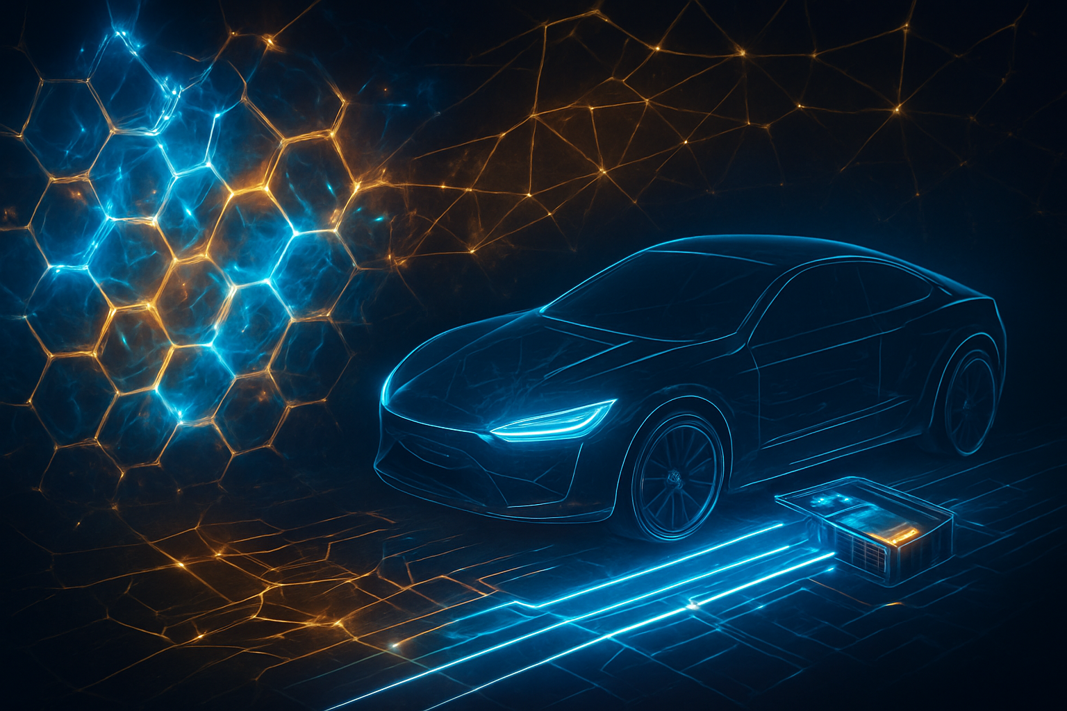
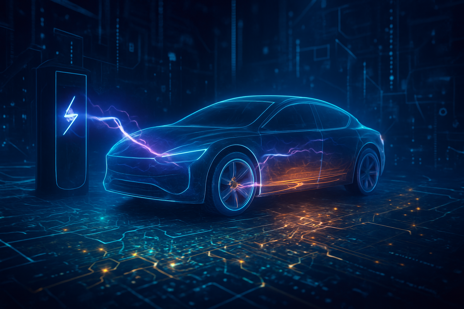
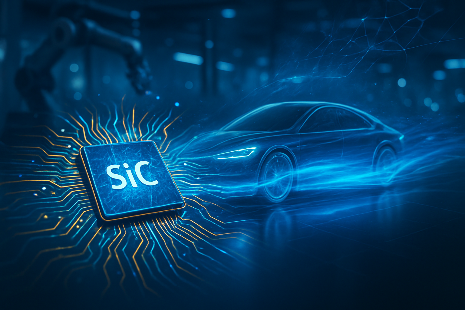
    As of late January 2026, the automotive landscape has reached a definitive turning point, moving away from the charging bottlenecks and range limitations of the early 2020s. The driving force behind this transformation is the rapid, global expansion of Silicon Carbide (SiC) semiconductors. These high-performance chips have officially supplanted traditional silicon as the backbone of the electric vehicle (EV) industry, enabling a widespread transition to 800V powertrain architectures that are redefining consumer expectations for mobility.

    The shift is no longer confined to luxury "halo" cars. In the first few weeks of 2026, major manufacturers have signaled that SiC-based 800V systems are now the standard for mid-range and premium models alike. This transition is crucial because it effectively doubles the voltage of the vehicle's electrical system, allowing for significantly faster charging times and higher efficiency. Industry data shows that SiC chips are now capturing over 80% of the 800V traction inverter market, a milestone that has fundamentally altered the competitive dynamics of the semiconductor industry.

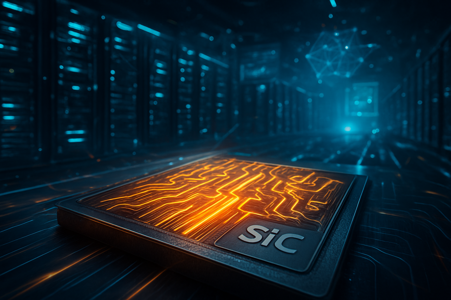
    Technical Superiority and the 200mm Breakthrough

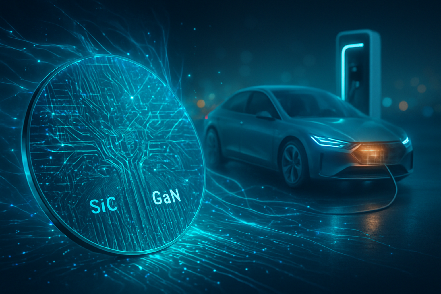
    At the heart of this revolution is the unique physical property of Silicon Carbide as a wide-bandgap (WBG) semiconductor. Unlike traditional Silicon (Si) IGBTs (Insulated-Gate Bipolar Transistors), SiC MOSFETs can operate at much higher temperatures, voltages, and switching frequencies. This allows for power inverters that are not only 10% to 15% smaller and lighter but also significantly more efficient. In 2026, these efficiency gains—typically ranging from 2% to 4%—are being leveraged to offset the massive power draw of the latest AI-driven autonomous driving suites, such as those powered by NVIDIA (NASDAQ: NVDA).

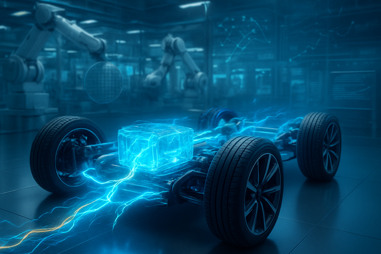
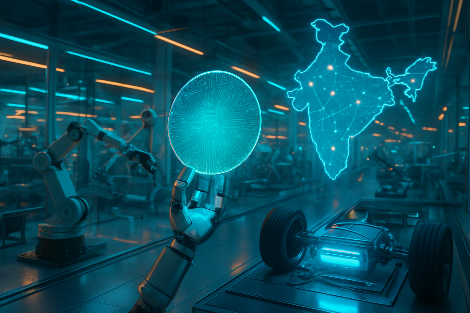
    The technical narrative of 2026 is dominated by the move to 200mm (8-inch) wafer production. For years, the industry struggled with 150mm wafers, which limited supply and kept costs high. However, the operational success of STMicroelectronics (NYSE: STM) and their new Catania "Silicon Carbide Campus" in Italy has changed the math. By achieving high-volume 200mm production this month, STMicroelectronics has drastically improved yields and reduced the cost-per-die, making SiC viable for mass-market vehicles. These chips allow the 2026 BMW (OTC: BMWYY) "Neue Klasse" models to achieve a 10% to 80% charge in just 21 minutes, while the Lucid (NASDAQ: LCID) Gravity is now clocking 200 miles of range in under 11 minutes.

    The Titans of Power: STMicroelectronics and Wolfspeed

    The expansion of SiC has created a new hierarchy among chipmakers. STMicroelectronics (NYSE: STM) has solidified its lead by becoming a vertically integrated powerhouse, controlling everything from raw SiC powder to finished power modules. Their recent expansion of a long-term supply agreement with Geely (OTC: GELYF) illustrates the strategic importance of this integration. By securing a guaranteed pipeline of 800V SiC components, Geely’s brands, including Volvo and Polestar, have gained a critical advantage in the race to offer the fastest-charging vehicles in the Chinese and European markets.

    Meanwhile, Wolfspeed (NYSE: WOLF) has pivoted to become the world's premier substrate supplier. Their John Palmour Manufacturing Center in North Carolina is now the largest SiC wafer fab on the planet, supplying the raw materials that other giants like Infineon and Onsemi (NASDAQ: ON) rely on. Wolfspeed's recent breakthrough in 300mm (12-inch) SiC wafer pilot lines, announced just last quarter, suggests that the cost of these advanced semiconductors will continue to plummet through 2028. This substrate dominance makes Wolfspeed an indispensable partner for nearly every major automotive player, including their ongoing development work with ZF Group to optimize e-axles for commercial trucking.

    Broader Implications for the AI and Energy Landscape

    The expansion of SiC is not just an automotive story; it is a critical component of the broader AI ecosystem. As vehicles transition into "Software-Defined Vehicles" (SDVs), the onboard AI processors required for Level 3 and Level 4 autonomy consume massive amounts of energy. The efficiency gains provided by SiC-based powertrains provide the necessary "power budget" to run these AI systems without sacrificing hundreds of miles of range. In early January 2026, NVIDIA (NASDAQ: NVDA) emphasized this synergy at CES, showcasing how their 800V power blueprints rely on SiC to manage the intense thermal and electrical loads of AI-driven navigation.

    Furthermore, the rise of SiC is easing the strain on global charging infrastructure. Because 800V SiC vehicles can charge at higher speeds (up to 350kW), they spend less time at charging stalls, effectively increasing the "throughput" of existing charging stations. This helps mitigate the "range anxiety" that has historically slowed EV adoption. However, this shift also brings concerns regarding the environmental impact of SiC manufacturing and the intense capital expenditure required to keep pace with the 300mm transition. Critics point out that while SiC makes vehicles more efficient, the energy-intensive process of growing SiC crystals remains a challenge for the industry’s carbon-neutral goals.

    The Horizon: 1200V Systems and Beyond

    Looking ahead to the remainder of 2026 and into 2027, the industry is already eyeing the next frontier: 1200V architectures. While 800V is currently the sweet spot for passenger cars, heavy-duty commercial vehicles and electric aerospace applications are demanding even higher voltages. Experts predict that the lessons learned from the 800V SiC rollout will accelerate the development of 1200V and even 1700V systems, potentially enabling electric long-haul trucking to become a reality by the end of the decade.

    The next 12 to 18 months will also see a push toward "Integrated Power Modules," where the SiC inverter, the motor, and the AI control unit are housed in a single, ultra-compact housing. Companies like Tesla (NASDAQ: TSLA) are expected to unveil further refinements to their proprietary SiC packaging, which could reduce the use of rare-earth materials and further lower the entry price for high-performance EVs. The challenge will remain supply chain resilience, as the world becomes increasingly dependent on a handful of high-tech fabs for its transport energy needs.

    Summary of the SiC Transformation

    The rapid expansion of Silicon Carbide in 2026 marks the end of the "early adopter" phase for high-voltage electric mobility. By solving the dual challenges of charging speed and energy efficiency, SiC has become the enabling technology for a new generation of vehicles that are as convenient as they are sustainable. The dominance of players like STMicroelectronics (NYSE: STM) and Wolfspeed (NYSE: WOLF) highlights the shift in value from traditional mechanical engineering to advanced power electronics.

    In the history of technology, the 2026 SiC boom will likely be viewed as the moment the electric vehicle finally overcame its last major hurdle. As we watch the first 200mm-native vehicle fleets hit the roads this spring, the focus will shift from "will EVs work?" to "how fast can we build them?" The 800V era is here, and it is paved with Silicon Carbide.


    This content is intended for informational purposes only and represents analysis of current AI and semiconductor developments.

    TokenRing AI delivers enterprise-grade solutions for multi-agent AI workflow orchestration, AI-powered development tools, and seamless remote collaboration platforms.
    For more information, visit https://www.tokenring.ai/.

  • The Power Revolution: AI and Wide-Bandgap Semiconductors Pave the Way for the $10B SiC Era

    The Power Revolution: AI and Wide-Bandgap Semiconductors Pave the Way for the $10B SiC Era

    As of January 23, 2026, the automotive industry has reached a pivotal tipping point in its electrification journey, driven by the explosive rise of wide-bandgap (WBG) materials. Silicon Carbide (SiC) and Gallium Nitride (GaN) have transitioned from high-end specialized components to the essential backbone of modern power electronics. This shift is not just a hardware upgrade; it is being accelerated by sophisticated artificial intelligence systems that are optimizing material discovery, manufacturing yields, and real-time power management. The global Silicon Carbide market is now firmly on a trajectory to surpass $10 billion by the end of the decade, as it systematically dismantles the long-standing dominance of traditional silicon-based semiconductors.

    The immediate significance of this development lies in the democratization of the 800V electric vehicle (EV) architecture. While 800V systems were previously reserved for luxury performance vehicles, the integration of SiC and GaN, paired with AI-driven design tools, has brought ultra-fast charging and extended range to mass-market models. For consumers, this means the era of the "15-minute charge" has finally arrived. For the tech industry, it represents the merging of advanced material science with AI-orchestrated manufacturing, creating a more resilient and efficient energy ecosystem.

    Engineering the 800V Standard: The WBG Technical Edge

    The transition from traditional Silicon (Si) Insulated Gate Bipolar Transistors (IGBTs) to Silicon Carbide and Gallium Nitride represents one of the most significant leaps in power electronics history. Unlike traditional silicon, SiC and GaN possess a much wider "bandgap"—the energy range where no electron states can exist. This physical property allows these materials to operate at much higher voltages, temperatures, and frequencies. Specifically, SiC’s thermal conductivity is roughly 3.5 times higher than silicon’s, enabling it to dissipate heat far more effectively and operate at temperatures exceeding 200°C.

    These technical specifications have profound implications for EV design. By moving to an 800V architecture enabled by SiC, automakers can double the voltage and halve the current required for the same power output. This allows for the use of thinner, lighter copper wiring—reducing vehicle weight by upwards of 30 pounds—and slashes internal resistance losses. Efficiency in power conversion has jumped from roughly 94% with silicon to over 99% with SiC and GaN. Furthermore, the high switching speeds of GaN (which can exceed 1 MHz) allow for significantly smaller inductors and capacitors, shrinking the overall size of on-board chargers and DC-DC converters by up to 50%.

    Initial reactions from the semiconductor research community have highlighted that the "yield wall" of WBG materials is finally being scaled. Historically, SiC was difficult to manufacture due to its extreme hardness and the complexity of growing defect-free crystals. However, the introduction of AI-driven predictive modeling in late 2024 and throughout 2025 has revolutionized the growth process. Industry experts at the 2026 Applied Power Electronics Conference (APEC) noted that AI-enhanced defect detection has boosted 200mm (8-inch) wafer yields by nearly 20%, making these materials economically viable for the first time for budget-tier vehicles.

    The Corporate Battlefield: Leaders in the $10B SiC Market

    The shift toward WBG materials has reorganized the competitive landscape for major semiconductor players. STMicroelectronics (NYSE: STM), currently the market leader in SiC device supply, has solidified its position through a massive integrated "SiC Campus" in Italy. By utilizing AI for real-time performance analytics across its global sites, STM has maintained a dominant share of the supply chain for leading EV manufacturers. Meanwhile, Wolfspeed (NYSE: WOLF) has emerged from its 2025 financial restructuring as a leaner, 200mm-focused powerhouse, leveraging AI-driven "Material Informatics" to discover new substrate compositions that improve reliability and lower costs.

    Other tech giants are rapidly positioning themselves to capture the burgeoning market. ON Semiconductor (NASDAQ: ON), also known as Onsemi, has focused on high-density packaging, using AI-simulated thermal models to cram more power into smaller modules. Infineon Technologies (OTC: IFNNY) has successfully launched its CoolSiC Gen2 line, which has become the standard for high-performance OEMs. Even Tesla (NASDAQ: TSLA), which famously announced a 75% reduction in SiC content per vehicle in 2023, has actually deepened the industry's sophistication; they are using custom AI Electronic Design Automation (EDA) tools to perform "chip-to-system co-design," allowing them to extract more performance from fewer, more power-dense SiC chips.

    This development is significantly disrupting existing products. Traditional silicon IGBT manufacturers are seeing their automotive order books evaporate as OEMs switch to WBG for all new platforms. Startups in the "GaN-on-Silicon" space are also benefiting, as they offer a lower-cost entry point for 400V systems and auxiliary power modules, putting pressure on legacy providers to pivot or face obsolescence. The market positioning now favors those who can integrate AI at the manufacturing level to ensure the highest possible reliability.

    Broader Significance: AI Integration and the Sustainability Mandate

    The rise of WBG materials is inextricably linked to the broader AI landscape. We are seeing a "double-ended" AI benefit: AI is used to design and build these chips, and these chips are, in turn, powering the high-voltage infrastructure needed for AI data centers. "Material Informatics"—the application of AI to material science—has cut the time needed for device modeling and Process Design Kit (PDK) development from years to months. This allows for rapid iteration of new chip architectures that can handle the massive energy demands of modern technological society.

    From a sustainability perspective, the impact is immense. Increasing EV efficiency by just 5% through SiC adoption is equivalent to removing millions of tons of CO2 from the atmosphere over the lifecycle of a global fleet. However, the transition is not without concerns. The manufacturing of SiC is significantly more energy-intensive than traditional silicon, leading some to question the "green-ness" of the production phase. Furthermore, the concentration of SiC substrate production in a handful of high-tech facilities has raised supply chain security concerns similar to those seen during the 2021 chip shortage.

    Comparatively, the shift to SiC is being viewed by historians as the "Silicon-to-Gallium" moment for the 21st century—reminiscent of the transition from vacuum tubes to transistors. It represents a fundamental change in the physics of our power systems, moving away from "managing heat" to "eliminating losses."

    The Road Ahead: AI on the Chip and Mass Adoption

    Looking toward 2027 and beyond, the next frontier is "AI on the chip." We are seeing the first generation of AI-driven gate drivers—chips that include embedded machine learning kernels to monitor the thermal health of a transistor in real-time. These smart drivers can predict a component failure before it happens and adjust switching patterns to mitigate damage or optimize efficiency on the fly. This predictive maintenance will be vital for the rollout of autonomous Robotaxis, where vehicle uptime is the most critical metric.

    Experts predict that as the SiC market crosses the $10 billion threshold, we will see a surge in "GaN-on-SiC" and even Diamond-based semiconductors for niche aerospace and extreme-environment applications. The near-term challenge remains the scale-up of 200mm wafer production. While yield rates are improving, the industry must continue to invest in automated, AI-controlled foundries to meet the projected demand of 30 million EVs per year by 2030.

    Summary and Outlook

    The transition to wide-bandgap materials like SiC and GaN, accelerated by AI, marks a definitive end to the "Silicon Age" for automotive power electronics. Key takeaways include the standardization of the 800V architecture, the use of AI to solve complex manufacturing hurdles, and the emergence of a multi-billion-dollar market led by players like STM, Wolfspeed, and Infineon.

    In the history of AI and technology, this development will be remembered as the moment when "Material Informatics" proved its value, turning a difficult-to-handle crystal into the engine of the global energy transition. In the coming weeks and months, watch for major announcements from mass-market automakers regarding 800V platform standardizations and further breakthroughs in AI-integrated power management systems. The power revolution is no longer coming; it is already here.


    This content is intended for informational purposes only and represents analysis of current AI developments.

    TokenRing AI delivers enterprise-grade solutions for multi-agent AI workflow orchestration, AI-powered development tools, and seamless remote collaboration platforms.
    For more information, visit https://www.tokenring.ai/.

  • The 800V Revolution: Silicon Carbide Demand Skyrockets as 2026 Becomes the ‘Year of the High-Voltage EV’

    The 800V Revolution: Silicon Carbide Demand Skyrockets as 2026 Becomes the ‘Year of the High-Voltage EV’

    As of January 2026, the automotive industry has reached a decisive turning point in the electrification race. The shift toward 800-volt (800V) architectures is no longer a luxury hallmark of high-end sports cars but has become the benchmark for the next generation of mass-market electric vehicles (EVs). At the center of this tectonic shift is a surge in demand for Silicon Carbide (SiC) power semiconductors—chips that are more efficient, smaller, and more heat-tolerant than the traditional silicon that powered the first decade of EVs.

    This demand surge has triggered a massive capacity race among global semiconductor leaders. Giants like STMicroelectronics (NYSE: STM) and Infineon Technologies (OTC: IFNNY) are ramping up 200mm (8-inch) wafer production at a record pace to meet the requirements of automotive leaders. These chips are not merely hardware components; they are the critical enabler for the "software-defined vehicle" (SDV), allowing carmakers to offset the massive power consumption of modern AI-driven autonomous driving systems with unprecedented powertrain efficiency.

    The Technical Edge: Efficiency, 200mm Wafers, and AI-Enhanced Yields

    The move to 800V systems is fundamentally a physics solution to the problems of charging speed and range. By doubling the voltage from the traditional 400V standard, automakers can reduce current for the same power delivery, which in turn allows for thinner, lighter copper wiring and significantly faster DC charging. However, traditional silicon IGBTs (Insulated-Gate Bipolar Transistors) struggle at these higher voltages due to energy loss and heat. SiC MOSFETs, with their wider bandgap, achieve inverter efficiencies exceeding 99% and generate up to 50% less heat, permitting 10% smaller and lighter cooling systems.

    The breakthrough for 2026, however, is not just the material but the manufacturing process. The industry is currently in the middle of a high-stakes transition from 150mm to 200mm (8-inch) wafers. This transition increases chip output per substrate by nearly 85%, which is vital for bringing SiC costs down to a level where mid-range EVs can compete with internal combustion engines. Furthermore, manufacturers have integrated advanced AI vision models and deep learning into their fabrication plants. By using Transformer-based vision systems to detect crystal defects during growth, companies like Wolfspeed (NYSE: WOLF) have increased yields to levels once thought impossible for this notoriously difficult material.

    Initial reactions from the semiconductor research community suggest that the 2026 ramp-up of 200mm SiC marks the end of the "supply constraint era" for wide-bandgap materials. Experts note that the ability to grow high-quality SiC crystals at scale—once a bottleneck that held back the entire EV industry—has finally caught up with the aggressive production schedules of the world’s largest automakers.

    Scaling for the Titans: STMicro and Infineon Lead the Capacity Charge

    The competitive landscape for power semiconductors has reshaped itself around massive "mega-fabs." STMicroelectronics is currently leading the charge with its fully integrated Silicon Carbide Campus in Catania, Italy. This €5 billion facility, supported by the EU Chips Act, has officially reached high-volume 200mm production this month. ST’s vertical integration—controlling the process from raw SiC powder to finished power modules—gives it a strategic advantage in supply security for its anchor partners, including Tesla and Geely Auto.

    Infineon Technologies is countering with its "Kulim 3" facility in Malaysia, which has been inaugurated as the world’s largest 200mm SiC power fab. Infineon’s "CoolSiC" technology is currently being deployed in the high-stakes launch of the Rivian (NASDAQ: RIVN) R2 platform and the continued expansion of Xiaomi’s EV lineup. By leveraging a "one virtual fab" strategy across its Malaysia and Villach, Austria locations, Infineon is positioning itself to capture a projected 30% of the global SiC market by the end of the decade.

    Other major players, such as Onsemi (NASDAQ: ON), have focused on the 800V ecosystem through their EliteSiC platform. Onsemi has secured massive multi-year deals with Tier-1 suppliers like Magna, positioning itself as the "energy bridge" between the powertrain and the digital cockpit. Meanwhile, Wolfspeed remains a wildcard; after a 2025 financial restructuring, it has emerged as a leaner, substrate-focused powerhouse, recently announcing a 300mm wafer breakthrough that could leapfrog current 200mm standards by 2028.

    The AI Synergy: Offsetting the 'Energy Tax' of Autonomy

    Perhaps the most significant development in 2026 is the realization that SiC is the "secret weapon" for AI-driven autonomous driving. As vehicles move toward Level 3 and Level 4 autonomy, the power consumption of on-board AI processors—like NVIDIA (NASDAQ: NVDA) DRIVE Thor—and their associated sensors has reached critical levels, often consuming between 1kW and 2.5kW of continuous power. This "energy tax" could historically reduce an EV's range by as much as 20%.

    The efficiency gains of SiC-based 800V powertrains provide a direct solution to this problem. By reclaiming energy typically lost as heat in the inverter, SiC can boost a vehicle's range by roughly 7% to 10% without increasing battery size. In effect, the energy saved by the SiC hardware is what "powers" the AI brains of the car. This synergy has made SiC a non-negotiable component for Software-Defined Vehicles (SDVs), where the cooling budget is increasingly allocated to the high-heat AI computers rather than the motor.

    This trend mirrors the broader evolution of the technology landscape, where hardware efficiency is becoming the primary bottleneck for AI deployment. Just as data centers are turning to liquid cooling and specialized power delivery, the automotive world is using SiC to ensure that "smart" cars do not become "short-range" cars.

    Future Horizons: 300mm Wafers and the Rise of GaN

    Looking toward 2027 and beyond, the industry is already eyeing the next frontier. While 200mm SiC is the standard for 2026, the first pilot lines for 300mm (12-inch) SiC wafers are expected to be announced by year-end. This shift would provide even more dramatic cost reductions, potentially bringing SiC to the $25,000 EV segment. Additionally, researchers are exploring "hybrid" systems that combine SiC for the main traction inverter with Gallium Nitride (GaN) for on-board chargers and DC-DC converters, maximizing efficiency across the entire electrical architecture.

    Experts predict that by 2030, the traditional silicon-based inverter will be entirely phased out of the passenger car market. The primary challenge remains the geopolitical concentration of the SiC supply chain, as both Europe and North America race to reduce reliance on Chinese raw material processing. The coming months will likely see more announcements regarding domestic substrate manufacturing as governments view SiC as a matter of national economic security.

    A New Foundation for Mobility

    The surge in Silicon Carbide demand in 2026 represents more than a simple supply chain update; it is the foundation for the next fifty years of transportation. By solving the dual challenges of charging speed and the energy demands of AI, SiC has cemented its status as the "silicon of the 21st century." The successful scale-up by STMicroelectronics, Infineon, and their peers has effectively decoupled EV performance from its previous limitations.

    As we look toward the remainder of 2026, the focus will shift from capacity to integration. Watch for how carmakers utilize the "weight credit" provided by 800V systems to add more advanced AI features, larger interior displays, and more robust safety systems. The high-voltage era has officially arrived, and it is paved with Silicon Carbide.


    This content is intended for informational purposes only and represents analysis of current AI and semiconductor developments.

    TokenRing AI delivers enterprise-grade solutions for multi-agent AI workflow orchestration, AI-powered development tools, and seamless remote collaboration platforms.
    For more information, visit https://www.tokenring.ai/.

  • The Power Revolution: How GaN and SiC Semiconductors are Electrifying the AI and EV Era

    The Power Revolution: How GaN and SiC Semiconductors are Electrifying the AI and EV Era

    The global technology landscape is currently undergoing its most significant hardware transformation since the invention of the silicon transistor. As of January 21, 2026, the transition from traditional silicon to Wide-Bandgap (WBG) semiconductors—specifically Gallium Nitride (GaN) and Silicon Carbide (SiC)—has reached a fever pitch. This "Power Revolution" is no longer a niche upgrade; it has become the fundamental backbone of the artificial intelligence boom and the mass adoption of 800V electric vehicle (EV) architectures. Without these advanced materials, the massive power demands of next-generation AI data centers and the range requirements of modern EVs would be virtually impossible to sustain.

    The immediate significance of this shift is measurable in raw efficiency and physical scale. In the first few weeks of 2026, we have seen the industry move from 200mm (8-inch) production standards to the long-awaited 300mm (12-inch) wafer milestone. This evolution is slashing the cost of high-performance power chips, bringing them toward price parity with silicon while delivering up to 99% system efficiency. As AI chips like NVIDIA’s latest "Rubin" architecture push past the 1,000-watt-per-chip threshold, the ability of GaN and SiC to handle extreme heat and high voltages in a fraction of the space is the only factor preventing a total energy grid crisis.

    Technical Milestones: Breaking the Silicon Ceiling

    The technical superiority of WBG semiconductors stems from their ability to operate at much higher voltages, temperatures, and frequencies than traditional silicon. Silicon Carbide (SiC) has established itself as the "muscle" for high-voltage traction in EVs, while Gallium Nitride (GaN) has emerged as the high-speed engine for data center power supplies. A major breakthrough announced in early January 2026 involves the widespread commercialization of Vertical GaN architecture. Unlike traditional lateral GaN, vertical structures allow devices to operate at 1200V and above, enabling a 30% increase in efficiency and a 50% reduction in the physical footprint of power supply units (PSUs).

    In the data center, these advancements have manifested in the move toward 800V High-Voltage Direct Current (HVDC) power stacks. By switching from AC to 800V DC, data center operators are minimizing conversion losses that previously plagued large-scale AI clusters. Modern GaN-based PSUs are now achieving record-breaking 97.5% peak efficiency, allowing a standard server rack to quadruple its power density. Where a legacy 3kW module once sat, engineers can now fit a 12kW unit in the same physical space. This miniaturization is further supported by "wire-bondless" packaging and silver sintering techniques that replace old-fashioned copper wiring with high-performance thermal interfaces.

    Initial reactions from the semiconductor research community have been overwhelmingly positive, with experts noting that the transition to 300mm single-crystal SiC wafers—first demonstrated by Wolfspeed early this month—is a "Moore's Law moment" for power electronics. The ability to produce 2.3 times more chips per wafer is expected to drive down costs by nearly 40% over the next 18 months. This technical leap effectively ends the era of silicon dominance in power applications, as the performance-to-cost ratio finally tips in favor of WBG materials.

    Market Impact: The New Power Players

    The shift to WBG semiconductors has sparked a massive realignment among chipmakers and tech giants. Wolfspeed (NYSE: WOLF), having successfully navigated a strategic restructuring in late 2025, has emerged as a vertically integrated leader in 200mm and 300mm SiC production. Their ability to control the supply chain from raw crystal growth to finished chips has given them a significant edge in the EV market. Similarly, STMicroelectronics (NYSE: STM) has ramped up production at its Catania campus to 15,000 wafers per week, securing its position as a primary supplier for European and American automakers.

    Other major beneficiaries include Infineon Technologies (OTC: IFNNY) and ON Semiconductor (NASDAQ: ON), both of whom have forged deep collaborations with NVIDIA (NASDAQ: NVDA). As AI "factories" require unprecedented amounts of electricity, NVIDIA has integrated these WBG-enabled power stacks directly into its reference designs. This "Grid-to-Processor" strategy ensures that the power delivery is as efficient as the computation itself. Startups in the GaN space, such as Navitas Semiconductor, are also seeing increased valuation as they disrupt the consumer electronics and onboard charger (OBC) markets with ultra-compact, high-speed switching solutions.

    This development is creating a strategic disadvantage for companies that have been slow to pivot away from silicon-based Insulated Gate Bipolar Transistors (IGBTs). While legacy silicon still holds the low-end consumer market, the high-margin sectors of AI and EVs are now firmly WBG-territory. Major tech companies are increasingly viewing power efficiency as a competitive "moat"—if a data center can run 20% more AI chips on the same power budget because of SiC and GaN, that company gains a massive lead in the ongoing AI arms race.

    Broader Significance: Sustaining the AI Boom

    The wider significance of the WBG revolution cannot be overstated; it is the "green" solution to a brown-energy problem. The AI industry has faced intense scrutiny over its massive electricity consumption, but the deployment of WBG semiconductors offers a tangible way to mitigate environmental impact. By reducing power conversion losses, these materials could save hundreds of terawatt-hours of electricity globally by the end of the decade. This aligns with the aggressive ESG (Environmental, Social, and Governance) targets set by tech giants who are struggling to balance their AI ambitions with carbon-neutrality goals.

    Historically, this transition is being compared to the shift from vacuum tubes to transistors. While the transistor allowed for the miniaturization of logic, WBG materials are allowing for the miniaturization and "greening" of power. However, concerns remain regarding the supply of raw materials like high-purity carbon and gallium, as well as the geopolitical tensions surrounding the semiconductor supply chain. Ensuring a stable supply of these "power minerals" is now a matter of national security for major economies.

    Furthermore, the impact on the EV industry is transformative. By making 800V architectures the standard, the "range anxiety" that has plagued EV adoption is rapidly disappearing. With SiC-enabled 500kW chargers, vehicles can now add 400km of range in just five minutes—the same time it takes to fill a gas tank. This parity with internal combustion engines is the final hurdle for mass-market EV transition, and it is being cleared by the physical properties of Silicon Carbide.

    The Horizon: From 1200V to Gallium Oxide

    Looking toward the near-term future, we expect the vertical GaN market to mature, potentially displacing SiC in certain mid-voltage EV applications. Researchers are also beginning to look beyond SiC and GaN toward Gallium Oxide (Ga2O3), an Ultra-Wide-Bandgap (UWBG) material that promises even higher breakdown voltages and lower losses. While Ga2O3 is still in the experimental phase, early prototypes suggest it could be the key to 3000V+ industrial power systems and future-generation electric aviation.

    In the long term, we anticipate a complete "power integration" where the power supply is no longer a separate brick but is integrated directly onto the same package as the processor. This "Power-on-Chip" concept, enabled by the high-frequency capabilities of GaN, could eliminate even more efficiency losses and lead to even smaller, more powerful AI devices. The primary challenge remains the cost of manufacturing and the complexity of thermal management at such extreme power densities, but experts predict that the 300mm wafer transition will solve the economics of this problem by 2027.

    Conclusion: A New Era of Efficiency

    The revolution in Wide-Bandgap semiconductors represents a fundamental shift in how the world manages and consumes energy. From the high-voltage demands of a Tesla or BYD to the massive computational clusters of an NVIDIA AI factory, GaN and SiC are the invisible heroes of the modern tech era. The milestones achieved in early 2026—specifically the transition to 300mm wafers and the rise of 800V HVDC data centers—mark the point of no return for traditional silicon in high-performance power applications.

    As we look ahead, the significance of this development in AI history will be seen as the moment hardware efficiency finally began to catch up with algorithmic demand. The "Power Revolution" has provided a lifeline to an industry that was beginning to hit a physical wall. In the coming weeks and months, watch for more automotive OEMs to announce the phase-out of 400V systems in favor of WBG-powered 800V platforms, and for data center operators to report significant energy savings as they upgrade to these next-generation power stacks.


    This content is intended for informational purposes only and represents analysis of current AI and semiconductor developments.

    TokenRing AI delivers enterprise-grade solutions for multi-agent AI workflow orchestration, AI-powered development tools, and seamless remote collaboration platforms.
    For more information, visit https://www.tokenring.ai/.

  • The Great Wide Bandgap Divide: SiC Navigates Oversupply as GaN Charges the AI Boom

    The Great Wide Bandgap Divide: SiC Navigates Oversupply as GaN Charges the AI Boom

    As of January 19, 2026, the global semiconductor landscape is witnessing a dramatic divergence in the fortunes of the two pillars of power electronics: Silicon Carbide (SiC) and Gallium Nitride (GaN). While the SiC sector is currently weathering a painful correction cycle defined by upstream overcapacity and aggressive price wars, GaN has emerged as the breakout star of the generative AI infrastructure gold rush. This "Power Revolution" is effectively decoupling high-performance electronics from traditional silicon, creating a new set of winners and losers in the race to electrify the global economy.

    The immediate significance of this shift cannot be overstated. With AI data centers now demanding power densities that traditional silicon simply cannot provide, and the automotive industry pivoting toward 800V fast-charging architectures, compound semiconductors have transitioned from niche "future tech" to the critical bottleneck of the 21st-century energy grid. The market dynamics of early 2026 reflect an industry in transition, moving away from the "growth at all costs" mentality of the early 2020s toward a more mature, manufacturing-intensive era where yield and efficiency are the primary drivers of stock valuation.

    The 200mm Baseline and the 300mm Horizon

    Technically, 2026 marks the official end of the 150mm (6-inch) era for high-performance applications. The transition to 200mm (8-inch) wafers has become the industry baseline, a move that has stabilized yields and finally achieved the long-awaited "cost-parity" with traditional silicon for mid-market electric vehicles. This shift was largely catalyzed by the operational success of major fabs like Wolfspeed's (NYSE: WOLF) Mohawk Valley facility and STMicroelectronics' (NYSE: STM) Catania campus, which have set new global benchmarks for scale. By increasing the number of chips per wafer by nearly 80%, the move to 200mm has fundamentally lowered the barrier to entry for wide bandgap (WBG) materials.

    However, the technical spotlight has recently shifted to Gallium Nitride, following Infineon's (OTC: IFNNY) announcement late last year regarding the operationalization of the world’s first 300mm power GaN production line. This breakthrough allows for a 2.3x higher chip yield per wafer compared to 200mm, setting a trajectory to make GaN as affordable as traditional silicon by 2027. This is particularly critical as AI GPUs, such as the latest NVIDIA (NASDAQ: NVDA) B300 series, now routinely exceed 1,000 watts per chip. Traditional silicon-based power supply units (PSUs) are too bulky and generate too much waste heat to handle these densities efficiently.

    Initial reactions from the research community emphasize that GaN-based PSUs are now achieving record-breaking 97.5% peak efficiency. This allows data center operators to replace legacy 3.3kW modules with 12kW units of the same physical footprint, effectively quadrupling power density. The industry consensus is that while SiC remains the king of high-voltage automotive traction, GaN is winning the "war of the rack" inside the AI data center, where high-frequency switching and compact form factors are the top priorities.

    Market Glut Meets the AI Data Center Boom

    The current state of the SiC market is one of "necessary correction." Following an unprecedented $20 billion global investment wave between 2019 and 2024, the industry is currently grappling with a significant oversupply. Global utilization rates for SiC upstream processes have dropped to between 50% and 70%, triggering an aggressive price war. Chinese suppliers, having captured over 40% of global wafer capacity, have forced prices for older 150mm wafers below production costs. This has placed immense pressure on Western firms, leading to strategic pivots and restructuring efforts across the board.

    Among the companies navigating this turmoil, onsemi (NASDAQ: ON) has emerged as a financial value play, successfully pivoting away from low-margin segments to focus on its high-performance EliteSiC M3e platform. Meanwhile, Navitas Semiconductor (NASDAQ: NVTS) has seen its stock soar following confirmed partnerships to provide 800V GaN architectures for next-generation AI data centers. Navitas has successfully transitioned from mobile fast-chargers to high-power infrastructure, positioning itself as a specialist in the AI power chain.

    The competitive implications are stark: major AI labs and hyperscalers like Microsoft (NASDAQ: MSFT) and Amazon (NASDAQ: AMZN) are now directly influencing semiconductor roadmaps to ensure they have the power modules necessary to keep their hardware cool and efficient. This shift gives a strategic advantage to vertically integrated players who can control the supply of raw wafers and the finished power modules, mitigating the volatility of the current overcapacity in the merchant wafer market.

    Wider Significance and the Path to Net Zero

    The broader significance of the GaN and SiC evolution lies in its role as a "decarbonization enabler." As the world struggles to meet Net Zero targets, the energy intensity of AI has become a focal point of environmental concern. The transition from silicon to compound semiconductors represents one of the most effective ways to reduce the carbon footprint of digital infrastructure. By cutting power conversion losses by 50% or more, these materials are effectively "finding" energy that would otherwise be wasted as heat, easing the burden on already strained global power grids.

    This milestone is comparable to the transition from vacuum tubes to transistors in the mid-20th century. We are no longer just improving performance; we are fundamentally changing the physics of how electricity is managed. However, potential concerns remain regarding the supply chain for materials like gallium and the geopolitical tensions surrounding the concentration of SiC processing in East Asia. As compound semiconductors become as strategically vital as advanced logic chips, they are increasingly being caught in the crosshairs of global trade policies and export controls.

    In the automotive sector, the SiC glut has paradoxically accelerated the democratization of EVs. With SiC prices falling, the 800V ultra-fast charging standard—once reserved for luxury models—is rapidly becoming the baseline for $35,000 mid-market vehicles. This is expected to drive a second wave of EV adoption as "range anxiety" is replaced by "charging speed confidence."

    Future Developments: Diamond Semiconductors and Beyond

    Looking toward 2027 and 2028, the next frontier is likely the commercialization of "Ultra-Wide Bandgap" materials, such as Diamond and Gallium Oxide. These materials promise even higher thermal conductivity and voltage breakdown limits, though they remain in the early pilot stages. In the near term, we expect to see the maturation of GaN-on-Silicon technology, which would allow GaN chips to be manufactured in standard CMOS fabs, potentially leading to a massive price collapse and the displacement of silicon even in low-power consumer electronics.

    The primary challenge moving forward will be addressing the packaging of these chips. As the chips themselves become smaller and more efficient, the physical wires and plastics surrounding them become the limiting factors in heat dissipation. Experts predict that "integrated power stages," where the gate driver and power switch are combined on a single chip, will become the standard design paradigm by the end of the decade, further driving down costs and complexity.

    A New Chapter in the Semiconductor Saga

    In summary, early 2026 is a period of "creative destruction" for the compound semiconductor industry. The Silicon Carbide sector is learning the hard lessons of cyclicality and overexpansion, while Gallium Nitride is experiencing its "NVIDIA moment," becoming indispensable to the AI revolution. The key takeaway for investors and industry watchers is that manufacturing scale and vertical integration have become the ultimate competitive moats.

    This development will likely be remembered as the moment power electronics became a Tier-1 strategic priority for the tech industry, rather than a secondary consideration. In the coming weeks, market participants should watch for further consolidation among mid-tier SiC players and the potential for a "standardization" of 800V architectures across the global automotive and data center sectors. The silicon age for power is over; the era of compound semiconductors has truly arrived.


    This content is intended for informational purposes only and represents analysis of current AI developments.

    TokenRing AI delivers enterprise-grade solutions for multi-agent AI workflow orchestration, AI-powered development tools, and seamless remote collaboration platforms.
    For more information, visit https://www.tokenring.ai/.

  • The End of the Silicon Age: How GaN and SiC are Electrifying the 2026 Green Energy Revolution

    The End of the Silicon Age: How GaN and SiC are Electrifying the 2026 Green Energy Revolution

    The global transition to sustainable energy has reached a pivotal tipping point this week as the foundational hardware of the electric vehicle (EV) industry undergoes its most significant transformation in decades. On January 14, 2026, Mitsubishi Electric (OTC: MIELY) announced it would begin shipping samples of its newest trench Silicon Carbide (SiC) MOSFET bare dies on January 21, marking a definitive shift away from traditional silicon-based power electronics. This development is not merely a marginal improvement; it represents a fundamental re-engineering of how energy is managed, moving the industry toward "wide-bandgap" (WBG) materials that promise to unlock unprecedented range for EVs and near-instantaneous charging speeds.

    As of early 2026, the era of "Good Enough" silicon is officially over for high-performance applications. The rapid deployment of Gallium Nitride (GaN) and Silicon Carbide (SiC) in everything from 800V vehicle architectures to 500kW ultra-fast chargers is slashing energy waste and enabling a leaner, more efficient "green" grid. With Mitsubishi’s latest shipment of 750V and 1200V trench-gate dies, the industry is witnessing a "50-70-90" shift: a 50% reduction in power loss compared to previous-gen SiC, a 70% reduction compared to traditional silicon, and a push toward 99% total system efficiency in power conversion.

    The Trench Revolution: Technical Leaps in Power Density

    The technical core of this transition lies in the move from "Planar" to "Trench" architectures in SiC MOSFETs. Mitsubishi Electric's new bare dies, including the 750V WF0020P-0750AA series, utilize a proprietary trench structure where gate electrodes are etched vertically into the wafer. This design drastically increases cell density and reduces "on-resistance," the primary culprit behind heat generation and energy loss. Unlike traditional Silicon Insulated-Gate Bipolar Transistors (Si-IGBTs), which have dominated the industry for 30 years, these SiC devices can handle significantly higher voltages and temperatures while maintaining a footprint that is nearly 60% smaller.

    Beyond SiC, Gallium Nitride (GaN) has made its own breakthrough into the 800V EV domain. Historically relegated to consumer electronics and low-power chargers, new "Vertical GaN" architectures launched in late 2025 now allow GaN to operate at 1200V+ levels. While SiC remains the "muscle" for the main traction inverters that drive a car's wheels, GaN has become the "speedster" for onboard chargers (OBC) and DC-DC converters. Because GaN can switch at frequencies in the megahertz range—orders of magnitude faster than silicon—it allows for much smaller passive components, such as transformers and inductors. This "miniaturization" has led to a 40% reduction in the weight of power electronics in 2026 model-year vehicles, directly translating to more miles per kilowatt-hour.

    Initial reactions from the power electronics community have been overwhelmingly positive. Dr. Elena Vance, a senior semiconductor analyst, noted that "the efficiency gains we are seeing with the 2026 trench-gate chips are the equivalent of adding 30-40 miles of range to an EV without increasing the battery size." Furthermore, the use of "Oblique Ion Implantation" in Mitsubishi's process has solved the long-standing trade-off between power loss and short-circuit robustness, a technical hurdle that had previously slowed the adoption of SiC in the most demanding automotive environments.

    A New Hierarchy: Market Leaders and the 300mm Race

    The shift to WBG materials has completely redrawn the competitive map of the semiconductor industry. STMicroelectronics (NYSE: STM) has solidified its lead as the dominant SiC supplier, capturing nearly 45% of the automotive market through its massive vertically integrated production hub in Catania, Italy. However, the most disruptive market move of 2026 came from Infineon Technologies (OTC: IFNNY), which recently operationalized the world’s first 300mm (12-inch) power GaN production line. This allows for a 2.3x higher chip yield per wafer, effectively commoditizing high-efficiency power chips that were once considered luxury components.

    The landscape also features a reborn Wolfspeed (NYSE: WOLF), which emerged from a 2025 restructuring as a "pure-play" SiC powerhouse. Operating the world’s largest fully automated 200mm fab in New York, Wolfspeed is now focusing on the high-end 1200V+ market required for heavy-duty trucking and AI data centers. Meanwhile, specialized players like Navitas Semiconductor (NASDAQ: NVTS) are dominating the "GaNFast" integrated circuit market, pushing the efficiency of 500kW fast chargers to the "Golden 99%" mark. This level of efficiency is critical because it eliminates the need for massive, expensive liquid cooling systems in chargers, allowing for slimmer, more reliable "plug-and-go" infrastructure.

    Strategic partnerships are also shifting. Automakers like Tesla (NASDAQ: TSLA) and BYD (OTC: BYDDF) are increasingly moving away from buying discrete components and are instead co-developing custom "power modules" with companies like onsemi (NASDAQ: ON). This vertical integration allows OEMs to optimize the thermal management of the SiC/GaN chips specifically for their unique chassis designs, further widening the gap between legacy manufacturers and the new "software-and-silicon" defined car companies.

    AI and the Grid: The Brains Behind the Power

    The "Green Energy Transition" is no longer just about better materials; it is increasingly about the intelligence controlling them. In 2026, the integration of Edge AI into power modules has become the standard. Mitsubishi's 1700V modules now feature Real-Time Control (RTC) circuits that use machine learning algorithms to predict and prevent short-circuits within nanoseconds. This "Smart Power" approach allows the system to push the SiC chips to their physical limits while maintaining a safety buffer that was previously impossible.

    This development fits into a broader trend where AI optimizes the entire energy lifecycle. In the 500kW fast chargers appearing at highway hubs this year, AI-driven switching optimization dynamically adjusts the frequency of the GaN/SiC switches based on the vehicle's state-of-charge and the grid's current load. This reduces "switching stress" and extends the lifespan of the charger by up to 30%. Furthermore, Deep Learning is now used in the manufacturing of these chips themselves; companies like Applied Materials use AI to scan SiC crystals for microscopic "killer defects," bringing the yield of high-voltage wafers closer to that of traditional silicon and lowering the cost for the end consumer.

    The wider significance of this shift cannot be overstated. By reducing the heat loss in power conversion, the world is effectively "saving" terawatts of energy that would have otherwise been wasted as heat. In an era where AI data centers are putting unprecedented strain on the electrical grid, the efficiency gains provided by SiC and GaN are becoming a critical pillar of global energy security, ensuring that the transition to EVs does not collapse the existing power infrastructure.

    Looking Ahead: The Road to 1.2MW and Beyond

    As we move deeper into 2026, the next frontier for WBG materials is the Megawatt Charging System (MCS) for commercial shipping and aviation. Experts predict that the 1700V and 3300V SiC MOSFETs currently being sampled by Mitsubishi and its peers will be the backbone of 1.2MW charging stations, capable of refilling a long-haul electric semi-truck in under 20 minutes. These high-voltage systems will require even more advanced "SBD-embedded" MOSFETs, which integrate Schottky Barrier Diodes directly into the chip to maximize power density.

    On the horizon, the industry is already looking toward "Gallium Oxide" (Ga2O3) as a potential successor to SiC in the 2030s, offering even wider bandgaps for ultra-high-voltage applications. However, for the next five years, the focus will remain on the maturation of the GaN-on-Silicon and SiC-on-SiC ecosystems. The primary challenge remains the supply chain of raw materials, particularly the high-purity carbon and silicon required for SiC crystal growth, leading many nations to designate these semiconductors as "critical strategic assets."

    A New Standard for a Greener Future

    The shipment of Mitsubishi Electric’s latest SiC samples this week is more than a corporate milestone; it is a signpost for the end of the Silicon Age in power electronics. The transition to GaN and SiC has enabled a 70% reduction in power losses, a 5-7% increase in EV range, and the birth of 500kW fast-charging networks that finally rival the convenience of gasoline.

    As we look toward the remainder of 2026, the key developments to watch will be the scaling of 300mm GaN production and the integration of these high-efficiency chips into the "smart grid." The significance of this breakthrough in technology history will likely be compared to the transition from vacuum tubes to transistors—a fundamental shift that makes the "impossible" (like a 600-mile range EV that charges in 10 minutes) a standard reality. The green energy transition is now being fueled by the smallest of switches, and they are faster, cooler, and more efficient than ever before.


    This content is intended for informational purposes only and represents analysis of current technology and market developments.

    TokenRing AI delivers enterprise-grade solutions for multi-agent AI workflow orchestration, AI-powered development tools, and seamless remote collaboration platforms.
    For more information, visit https://www.tokenring.ai/.

  • The 1,000,000-Watt Rack: Mitsubishi Electric Breakthrough in Trench SiC MOSFETs Solves AI’s Power Paradox

    The 1,000,000-Watt Rack: Mitsubishi Electric Breakthrough in Trench SiC MOSFETs Solves AI’s Power Paradox

    In a move that signals a paradigm shift for high-density computing and sustainable transport, Mitsubishi Electric Corp (TYO: 6503) has announced a major breakthrough in Wide-Bandgap (WBG) power semiconductors. On January 14, 2026, the company revealed it would begin sample shipments of its next-generation trench Silicon Carbide (SiC) MOSFET bare dies on January 21. These chips, which utilize a revolutionary "trench" architecture, represent a 50% reduction in power loss compared to traditional planar SiC devices, effectively removing one of the primary thermal bottlenecks currently capping the growth of artificial intelligence and electric vehicle performance.

    The announcement comes at a critical juncture as the technology industry grapples with the energy-hungry nature of generative AI. With the latest AI-accelerated server racks now demanding up to 1 megawatt (1MW) of power, traditional silicon-based power conversion has hit a physical "efficiency wall." Mitsubishi Electric's new trench SiC technology is designed to operate in these extreme high-density environments, offering superior heat resistance and efficiency that allows power modules to shrink in size while handling significantly higher voltages. This development is expected to accelerate the deployment of next-generation data centers and extend the range of electric vehicles (EVs) by as much as 7% through more efficient traction inverters.

    Technical Superiority: The Trench Architecture Revolution

    At the heart of Mitsubishi Electric’s breakthrough is the transition from a "planar" gate structure to a "trench" design. In a traditional planar MOSFET, electricity flows horizontally across the surface of the chip before moving vertically, a path that inherently creates higher resistance and limits chip density. Mitsubishi’s new trench SiC-MOSFETs utilize a proprietary "oblique ion implantation" method. By implanting nitrogen in a specific diagonal orientation, the company has created a high-concentration layer that allows electricity to flow more easily through vertical channels. This innovation has resulted in a world-leading specific ON-resistance of approximately 1.84 mΩ·cm², a metric that translates directly into lower heat generation and higher efficiency.

    Technical specifications for the initial four models (WF0020P-0750AA through WF0080P-0750AA) indicate a rated voltage of 750V with ON-resistance ranging from 20 mΩ to 80 mΩ. Beyond mere efficiency, Mitsubishi has solved the "reliability gap" that has long plagued trench SiC devices. Trench structures are notorious for concentrated electric fields at the bottom of the "V" or "U" shape, which can degrade the gate-insulating film over time. To counter this, Mitsubishi engineers developed a unique electric-field-limiting structure by vertically implanting aluminum at the bottom of the trench. This protective layer reduces field stress to levels comparable to older planar devices, ensuring a stable lifecycle even under the high-speed switching demands of AI power supply units (PSUs).

    The industry reaction has been overwhelmingly positive, with power electronics researchers noting that Mitsubishi's focus on bare dies is a strategic masterstroke. By providing the raw chips rather than finished modules, Mitsubishi is allowing companies like NVIDIA Corp (NASDAQ: NVDA) and high-end EV manufacturers to integrate these power-dense components directly into custom liquid-cooled power shelves. Experts suggest that the 50% reduction in switching losses will be the deciding factor for engineers designing the 12kW+ power supplies required for the latest "Rubin" class GPUs, where every milliwatt saved reduces the massive cooling overhead of 1MW data center racks.

    Market Warfare: The Race for 200mm Dominance

    The release of these trench MOSFETs places Mitsubishi Electric in direct competition with a field of energized rivals. STMicroelectronics (NYSE: STM) currently holds the largest market share in the SiC space and is rapidly scaling its own 200mm (8-inch) wafer production in Italy and China. Similarly, Infineon Technologies AG (OTC: IFNNY) has recently brought its massive Kulim, Malaysia fab online, focusing on "CoolSiC" Gen2 trench devices. However, Mitsubishi’s proprietary gate oxide stability and its "bare die first" delivery strategy for early 2026 may give it a temporary edge in the high-performance "boutique" sector of the market, specifically for 800V EV architectures.

    The competitive landscape is also seeing a resurgence from Wolfspeed, Inc. (NYSE: WOLF), which recently emerged from a major restructuring to focus exclusively on its Mohawk Valley 8-inch fab. Meanwhile, ROHM Co., Ltd. (TYO: 6963) has been aggressive in the Japanese and Chinese markets with its 5th-generation trench designs. Mitsubishi’s entry into mass-production sample shipments marks a "normalization" of the 200mm SiC era, where increased yields are finally beginning to lower the "SiC tax"—the premium price that has historically kept Wide-Bandgap materials out of mid-range consumer electronics.

    Strategically, Mitsubishi is positioning itself as the go-to partner for the Open Compute Project (OCP) standards. As hyperscalers like Google and Meta move toward 1MW racks, they are shifting from 48V DC power distribution to high-voltage DC (HVDC) systems of 400V or 800V. Mitsubishi’s 750V-rated trench dies are perfectly positioned for the DC-to-DC conversion stages in these environments. By drastically reducing the footprint of the power infrastructure—sometimes by as much as 75% compared to silicon—Mitsubishi is enabling data center operators to pack more compute into the same physical square footage, a move that is essential for the survival of the current AI boom.

    Beyond the Chips: Solving the AI Sustainability Crisis

    The broader significance of this breakthrough cannot be overstated: it is a direct response to the "AI Power Crisis." The current generation of AI hardware, such as the Advanced Micro Devices, Inc. (NASDAQ: AMD) Instinct MI355X and NVIDIA’s Blackwell systems, has pushed the power density of data centers to a breaking point. A single AI rack in 2026 can consume as much electricity as a small town. Without the efficiency gains provided by Wide-Bandgap materials like SiC, the thermal load would require cooling systems so massive they would negate the economic benefits of the AI models themselves.

    This milestone is being compared to the transition from vacuum tubes to transistors in the mid-20th century. Just as the transistor allowed for the miniaturization of computers, SiC is allowing for the "miniaturization of power." By achieving 98% efficiency in power conversion, Mitsubishi's technology ensures that less energy is wasted as heat. This has profound implications for global sustainability goals; even a 1% increase in efficiency across the global data center fleet could save billions of kilowatt-hours annually.

    However, the rapid shift to SiC is not without concerns. The industry remains wary of supply chain bottlenecks, as the raw material—silicon carbide boules—is significantly harder to grow than standard silicon. Furthermore, the high-speed switching of SiC can create electromagnetic interference (EMI) issues in sensitive AI server environments. Mitsubishi’s unique gate oxide manufacturing process aims to address some of these reliability concerns, but the integration of these high-frequency components into existing legacy infrastructure remains a challenge for the broader engineering community.

    The Horizon: 2kV Chips and the End of Silicon

    Looking toward the late 2020s, the roadmap for trench SiC technology points toward even higher voltages and more extreme integration. Experts predict that Mitsubishi and its competitors will soon debut 2kV and 3.3kV trench MOSFETs, which would revolutionize the electrical grid itself. These devices could lead to "Solid State Transformers" that are a fraction of the size of current neighborhood transformers, enabling a more resilient and efficient smart grid capable of handling the intermittent nature of renewable energy sources like wind and solar.

    In the near term, we can expect to see these trench dies appearing in "Fusion" power modules that combine the best of Silicon and Silicon Carbide to balance cost and performance. Within the next 12 to 18 months, the first consumer EVs featuring these Mitsubishi trench dies are expected to hit the road, likely starting with high-end performance models that require the 20mΩ ultra-low resistance for maximum acceleration and fast-charging capabilities. The challenge for Mitsubishi will be scaling production fast enough to meet the insatiable demand of the "Mag-7" tech giants, who are currently buying every high-efficiency power component they can find.

    The industry is also watching for the potential "GaN-on-SiC" (Gallium Nitride on Silicon Carbide) hybrid chips. While SiC dominates the high-voltage EV and data center market, GaN is making inroads in lower-voltage consumer applications. The ultimate "holy grail" for power electronics would be a unified architecture that utilizes Mitsubishi's trench SiC for the main power stage and GaN for the ultra-high-frequency control stages, a development that researchers believe is only a few years away.

    A New Era for High-Power AI

    In summary, Mitsubishi Electric's announcement of trench SiC-MOSFET sample shipments marks a definitive end to the "Planar Era" of power semiconductors. By achieving a 50% reduction in power loss and solving the thermal reliability issues of trench designs, Mitsubishi has provided the industry with a vital tool to manage the escalating power demands of the AI revolution and the transition to 800V electric vehicle fleets. These chips are not just incremental improvements; they are the enabling hardware for the 1MW data center rack.

    As we move through 2026, the significance of this development will be felt across the entire tech ecosystem. For AI companies, it means more compute per watt. For EV owners, it means faster charging and longer range. And for the planet, it represents a necessary step toward decoupling technological progress from exponential energy waste. Watch for the results of the initial sample evaluations in the coming months; if the 20mΩ dies perform as advertised in real-world "Rubin" GPU clusters, Mitsubishi Electric may find itself at the center of the next great hardware gold rush.


    This content is intended for informational purposes only and represents analysis of current AI developments.

    TokenRing AI delivers enterprise-grade solutions for multi-agent AI workflow orchestration, AI-powered development tools, and seamless remote collaboration platforms.
    For more information, visit https://www.tokenring.ai/.


    Published on January 16, 2026.

  • The Silicon Pulse: How AI-Optimized Silicon Carbide is Reshaping the Global EV Landscape

    The Silicon Pulse: How AI-Optimized Silicon Carbide is Reshaping the Global EV Landscape

    As of January 2026, the global transition to electric vehicles (EVs) has reached a pivotal milestone, driven not just by battery chemistry, but by a revolution in power electronics. The widespread adoption of Silicon Carbide (SiC) has officially ended the era of traditional silicon-based power systems in high-performance and mid-market vehicles. This shift, underpinned by a massive scaling of production from industry leaders and the integration of AI-driven power management, has fundamentally altered the economics of the automotive industry. By enabling 800V architectures to become the standard for vehicles under $40,000, SiC technology has effectively eliminated "range anxiety" and "charging dread," paving the way for the next phase of global electrification.

    The immediate significance of this development lies in the unprecedented convergence of hardware efficiency and software intelligence. While SiC provides the physical ability to handle higher voltages and temperatures with minimal energy loss, new AI-optimized thermal management systems are now capable of predicting load demands in real-time, adjusting switching frequencies to squeeze every possible mile out of a battery pack. For the consumer, this translates to 10-minute charging sessions and an average range increase of 10% compared to previous generations, marking 2026 as the year EVs finally achieved total operational parity with internal combustion engines.

    The technical superiority of Silicon Carbide over traditional Silicon (Si) stems from its wider bandgap, which allows it to operate at significantly higher voltages, temperatures, and switching frequencies. In January 2026, the industry has successfully transitioned to 200mm (8-inch) wafer production as the baseline standard. This move from 150mm wafers has been the "holy grail" of the mid-2020s, providing a 1.8x increase in working chips per wafer and driving down per-unit costs by nearly 40%. Leading the charge, STMicroelectronics (NYSE:STM) has reached full mass-production capacity at its Catania Silicon Carbide Campus in Italy. This facility represents the world’s first fully vertically integrated SiC site, managing the entire lifecycle from raw powder to finished power modules, ensuring a level of quality control and supply chain resilience that was previously impossible.

    Technical specifications for 2026 models highlight the impact of this hardware. New 4th Generation STPOWER SiC MOSFETs feature drastically reduced on-resistance ($R_{DS(on)}$), which minimizes heat generation during the high-speed energy transfers required for 800V charging. This differs from previous Silicon IGBT technology, which suffered from significant "switching losses" and required massive, heavy cooling systems. By contrast, SiC-based inverters are 50% smaller and 30% lighter, allowing engineers to reclaim space for larger cabins or more aerodynamic designs. Industry experts and the power electronics research community have hailed the recent stability of 200mm yields as the "industrialization of a miracle material," noting that the defect rates in SiC crystals—long a hurdle for the industry—have finally reached automotive-grade reliability levels across all major suppliers.

    The shift to SiC has created a new hierarchy among semiconductor giants and automotive OEMs. STMicroelectronics currently holds a dominant market share of approximately 35-40%, largely due to its long-standing partnership with Tesla (NASDAQ:TSLA) and a strategic joint venture with Sanan Optoelectronics in China. This JV has successfully ramped up to 480,000 wafers annually, securing ST’s position in the world’s largest EV market. Meanwhile, Infineon Technologies (ETR:IFX) has asserted its dominance in the manufacturing space with its Kulim Mega-Fab in Malaysia, now the world’s largest 200mm SiC power semiconductor facility. Infineon’s recent demonstration of a 300mm (12-inch) pilot line in Villach, Austria, has sent shockwaves through the market, signaling that even greater cost reductions are on the horizon.

    Other major players like onsemi (NASDAQ:ON) have solidified their standing through multi-year supply agreements with the Volkswagen Group (XETRA:VOW3) and Hyundai-Kia. The strategic advantage now lies with companies that can provide "vertical integration"—owning the substrate production as well as the chip design. This has led to a competitive squeeze for smaller startups and traditional silicon suppliers who failed to pivot early enough. Wolfspeed (NYSE:WOLF), despite a difficult financial restructuring in late 2025, remains a critical lynchpin as a primary supplier of high-quality SiC substrates to the rest of the industry. The disruption is also felt in the charging infrastructure sector, where companies are being forced to upgrade to SiC-based ultra-fast 500kW chargers to support the new 800V vehicle fleets.

    Beyond the technical and corporate maneuvering, the SiC revolution is a cornerstone of the broader "Intelligent Edge" trend in AI and energy. In 2026, we are seeing the emergence of "AI-Power Fusion," where machine learning models are embedded directly into the motor control units. These AI agents use the high-frequency switching capabilities of SiC to perform "micro-optimizations" thousands of times per second, adjusting the power flow based on road conditions, battery health, and driver behavior. This level of granular control was physically impossible with older silicon hardware, which couldn't switch fast enough without overheating.

    This advancement fits into a larger global narrative of sustainable AI. As data centers and EVs both demand more power, the efficiency of SiC becomes an environmental necessity. By reducing the energy wasted as heat, SiC-equipped EVs are effectively reducing the total load on the power grid. However, concerns remain regarding the concentration of the supply chain. With a handful of companies and regions (notably Italy, Malaysia, and China) controlling the bulk of SiC production, geopolitical tensions continue to pose a risk to the "green transition." Comparisons are already being made to the early days of the microprocessor boom; just as silicon defined the 20th century, Silicon Carbide is defining the 21st-century energy landscape.

    Looking forward, the roadmap for Silicon Carbide is focused on the "300mm Frontier." While 200mm is the current standard, the transition to 300mm wafers—led by Infineon—is expected to reach high-volume commercialization by 2028, potentially cutting EV drivetrain costs by another 20-30%. On the horizon, we are also seeing the first pilot programs for 1500V systems, pioneered by BYD Company (HKEX:1211). These ultra-high-voltage systems could enable heavy-duty trucking and even short-haul electric aviation to become commercially viable by the end of the decade.

    The integration of AI into the manufacturing process itself is another key development. Companies are now using generative AI to design the next generation of SiC crystal growth furnaces, aiming to eliminate the remaining lattice defects that can lead to chip failure. The primary challenge remains the raw material supply; as demand for SiC expands into renewable energy grids and industrial automation, the race to secure high-quality carbon and silicon sources will intensify. Experts predict that by 2030, SiC will not just be an "EV chip," but the universal backbone of the global electrical infrastructure.

    The Silicon Carbide revolution represents one of the most significant shifts in the history of power electronics. By successfully scaling production and moving to the 200mm wafer standard, companies like STMicroelectronics and Infineon have removed the final barriers to mass-market EV adoption. The combination of faster charging, longer range, and lower costs has solidified the electric vehicle’s position as the primary mode of transportation for the future.

    As we move through 2026, keep a close watch on the progress of Infineon’s 300mm pilot lines and the expansion of STMicroelectronics' Chinese joint ventures. These developments will dictate the pace of the next wave of price cuts in the EV market. The "Silicon Pulse" is beating faster than ever, and it is powered by a material that was once considered too difficult to manufacture, but is now the very engine of the electric revolution.


    This content is intended for informational purposes only and represents analysis of current AI and technology developments.

    TokenRing AI delivers enterprise-grade solutions for multi-agent AI workflow orchestration, AI-powered development tools, and seamless remote collaboration platforms.
    For more information, visit https://www.tokenring.ai/.

  • The Silicon Carbide Surge: How STMicroelectronics and Infineon Are Powering the 2026 EV Revolution

    The Silicon Carbide Surge: How STMicroelectronics and Infineon Are Powering the 2026 EV Revolution

    The electric vehicle (EV) industry has reached a historic turning point this January 2026, as the "Silicon Carbide (SiC) Revolution" finally moves from luxury experimentation to mass-market reality. While traditional silicon has long been the workhorse of the electronics world, its physical limitations in high-voltage environments have created a bottleneck for EV range and charging speeds. Today, the massive scaling of SiC production by industry titans has effectively shattered those limits, enabling a new generation of vehicles that charge faster than a smartphone and travel further than their internal combustion predecessors.

    The immediate significance of this shift cannot be overstated. By transitioning to 200mm (8-inch) wafer production, leading semiconductor firms have slashed costs and boosted yields, allowing SiC-based power modules to be integrated into mid-market EVs priced under $40,000. This breakthrough is the "invisible engine" behind the 2026 model year's most impressive specs, including the first widespread rollout of 800-volt architectures that allow drivers to add 400 kilometers of range in less than five minutes.

    Technically, Silicon Carbide is a "wide-bandgap" (WBG) semiconductor, meaning it can operate at much higher voltages, temperatures, and frequencies than standard silicon. In the context of an EV, this allows for the creation of power inverters—the components that convert battery DC power to motor AC power—that are significantly more efficient. As of early 2026, the latest Generation-3 SiC MOSFETs from STMicroelectronics (NYSE: STM) and the CoolSiC Gen 2 line from Infineon Technologies (FWB: IFX) have achieved powertrain efficiencies exceeding 99%.

    This efficiency is not just a laboratory metric; it translates directly to thermal management. Because SiC generates up to 50% less heat during power switching than traditional silicon, the cooling systems in 2026 EVs are roughly 10% lighter and smaller. This creates a vicious cycle of weight reduction: a lighter cooling system allows for a lighter chassis, which in turn increases the vehicle's range. Current data shows that SiC-equipped vehicles are achieving an average 7% range increase over 2023 models without any increase in battery size.

    Furthermore, the transition to 200mm wafers has been the industry's "Holy Grail." Previously, most SiC was manufactured on 150mm (6-inch) wafers, which were prone to higher defect rates and lower output. The successful scaling to 200mm in late 2025 has increased usable chips per wafer by nearly 85%. This manufacturing milestone, supported by AI-driven defect detection and predictive fab management, has finally brought the price of SiC modules close to parity with high-end silicon components.

    The competitive landscape of 2026 is dominated by a few key players who moved early to secure their supply chains. STMicroelectronics has solidified its lead through a "Silicon Carbide Campus" in Catania, Italy, which handles the entire production cycle from raw powder to finished modules. Their joint venture with Sanan Optoelectronics in China has also reached full capacity, churning out 480,000 wafers annually to meet the insatiable demand of the Chinese EV market. ST’s early partnership with Tesla and recent major deals with Geely and Hyundai have positioned them as the primary backbone of the global EV fleet.

    Infineon Technologies has countered with its "One Virtual Fab" strategy, leveraging massive expansions in Villach, Austria, and Kulim, Malaysia. Their recent multi-billion dollar agreement with Stellantis (NYSE: STLA) to standardize power modules across 14 brands has effectively locked out smaller competitors from a significant portion of the European market. Infineon's focus on "CoolSiC" technology has also made them the preferred partner for high-performance entrants like Xiaomi (HKG: 1810), whose latest SU7 models utilize Infineon modules to achieve record-breaking acceleration and charging metrics.

    This production surge is causing significant disruption for traditional power semiconductor makers who were late to the SiC transition. Companies that relied on aging silicon-based Insulated-Gate Bipolar Transistors (IGBTs) are finding themselves relegated to the low-end, budget vehicle market. Meanwhile, the strategic advantage has shifted toward vertically integrated companies—those that own everything from the SiC crystal growth to the final module packaging—as they are better insulated from the supply shocks that plagued the industry earlier this decade.

    The broader significance of the SiC surge extends far beyond the driveway. This technology is a critical component of the global push for decarbonization and energy independence. As EV adoption accelerates thanks to SiC-enabled charging convenience, the demand for fossil fuels is seeing its most significant decline in history. Moreover, the high-frequency switching capabilities of SiC are being applied to the "Smart Grid," allowing for more efficient integration of renewable energy sources like solar and wind into the national electricity supply.

    However, the rapid shift has raised concerns regarding material sourcing. Silicon carbide requires high-purity carbon and silicon, and the manufacturing process is incredibly energy-intensive. There are also geopolitical implications, as the race for SiC dominance has led to "semiconductor nationalism," with the US, EU, and China all vying to subsidize local production hubs. This has mirrored previous milestones in the AI chip race, where control over manufacturing capacity has become a matter of national security.

    In terms of market impact, the democratization of 800-volt charging is the most visible breakthrough for the general public. It effectively addresses "range anxiety" and "wait-time anxiety," which were the two largest hurdles for EV adoption in the early 2020s. By early 2026, the infrastructure and the vehicle technology have finally synchronized, creating a user experience that is finally comparable—if not superior—to the traditional gas station model.

    Looking ahead, the next frontier for SiC is the potential transition to 300mm (12-inch) wafers, which would represent another massive leap in production efficiency. While currently in the pilot phase at firms like Infineon, full-scale 300mm production is expected by the late 2020s. We are also beginning to see the integration of SiC with Gallium Nitride (GaN) in "hybrid" power systems, which could lead to even smaller onboard chargers and DC-DC converters for the next generation of software-defined vehicles.

    Experts predict that the lessons learned from scaling SiC will be applied to other advanced materials, potentially accelerating the development of solid-state batteries. The primary challenge remaining is the recycling of these advanced power modules. As the first generation of SiC-heavy vehicles reaches the end of its life toward the end of this decade, the industry will need to develop robust methods for recovering and reusing these specialized materials.

    The Silicon Carbide revolution of 2026 is more than just an incremental upgrade; it is the fundamental technological shift that has made the electric vehicle a viable reality for the global majority. Through the aggressive scaling efforts of STMicroelectronics and Infineon, the industry has successfully moved past the "prototyping" phase of high-performance electrification and into a high-volume, high-efficiency era.

    The key takeaway for 2026 is that the powertrain is no longer a commodity—it is a sophisticated platform for innovation. As we watch the market evolve in the coming months, the focus will likely shift toward software-defined power management, where AI algorithms optimize SiC switching in real-time to squeeze every possible kilometer out of the battery. For now, the "SiC Surge" stands as one of the most significant engineering triumphs of the mid-2020s, forever changing how the world moves.


    This content is intended for informational purposes only and represents analysis of current AI and semiconductor developments.

    TokenRing AI delivers enterprise-grade solutions for multi-agent AI workflow orchestration, AI-powered development tools, and seamless remote collaboration platforms.
    For more information, visit https://www.tokenring.ai/.

  • India’s Silicon Ambition: Tata and ROHM Forge Strategic Alliance as Semiconductor Mission Hits High Gear

    India’s Silicon Ambition: Tata and ROHM Forge Strategic Alliance as Semiconductor Mission Hits High Gear

    As of January 12, 2026, India’s quest to become a global semiconductor powerhouse has reached a critical inflection point. The partnership between Tata Electronics and ROHM Co., Ltd. (TYO: 6963) marks a definitive shift from theoretical policy to high-stakes industrial execution. By focusing on automotive power MOSFETs—the literal workhorses of the electric vehicle (EV) revolution—this collaboration is positioning India not just as a consumer of chips, but as a vital node in the global silicon supply chain.

    This development is the centerpiece of the India Semiconductor Mission (ISM) 2.0, a $20 billion federal initiative designed to insulate the nation from global supply shocks while capturing a significant share of the burgeoning green energy and automotive markets. With the automotive industry rapidly electrifying, the localized production of power semiconductors is no longer a luxury; it is a strategic necessity for India’s economic sovereignty and its goal of becoming a $100 billion semiconductor market by 2030.

    Technical Precision: The Power Behind the EV Revolution

    The initial phase of the Tata-ROHM partnership centers on the production of an automotive-grade N-channel 100V, 300A Silicon (Si) MOSFET. These components are housed in a specialized TO-Leadless (TOLL) package, which offers superior thermal management and a significantly smaller footprint compared to traditional packaging. This technical specification is critical for modern EV architectures, where space is at a premium and heat dissipation is the primary barrier to battery efficiency. By utilizing ROHM’s advanced design and process expertise, Tata Electronics is bypassing the initial "learning curve" that often plagues new entrants in the semiconductor space.

    Beyond standard silicon, the roadmap for this partnership is paved with Wide-Bandgap (WBG) materials, specifically Silicon Carbide (SiC) and Gallium Nitride (GaN). These materials represent the cutting edge of power electronics, allowing for higher voltage operation and up to 50% less energy loss compared to traditional silicon-based chips. The technical transfer from ROHM—a global leader in SiC technology—ensures that India’s manufacturing capabilities will be future-proofed against the next generation of power-hungry applications, from high-speed rail to advanced renewable energy grids.

    The infrastructure supporting this technical leap is equally impressive. Tata Electronics is currently finalizing its $3 billion Outsourced Semiconductor Assembly and Test (OSAT) facility in Jagiroad, Assam. This site is slated for pilot production by mid-2026, serving as the primary hub for the ROHM-designed MOSFETs. Meanwhile, the $11 billion Dholera Fab in Gujarat, a joint venture between Tata and Taiwan’s PSMC, is moving toward its goal of producing 28nm to 110nm nodes, providing the "front-end" fabrication capacity that will eventually complement the backend packaging efforts.

    Disrupting the Global Supply Chain: Market Impacts

    The implications for the global semiconductor market are profound. For years, the industry has looked for a "China+1" alternative, and India is now presenting a credible, large-scale solution. The Tata-ROHM alliance directly benefits Tata Motors Ltd. (NSE: TATAMOTORS), which can now look forward to a vertically integrated supply chain for its EV lineup. This reduces lead times and protects the company from the volatility of the international chip market, providing a significant competitive advantage over global rivals who remain dependent on East Asian foundries.

    Furthermore, the emergence of India as a packaging hub is attracting other major players. Micron Technology, Inc. (NASDAQ: MU) is already nearing commercial production at its Sanand facility, and CG Power & Industrial Solutions (NSE: CGPOWER), in partnership with Renesas, is transitioning from pilot to commercial-scale operations. This cluster effect is creating a competitive ecosystem where startups and established giants alike can find the infrastructure needed to scale. For global chipmakers, the message is clear: India is no longer just a design center for the likes of Intel (NASDAQ: INTC) or NVIDIA (NASDAQ: NVDA); it is becoming a manufacturing destination.

    However, this disruption comes with challenges for existing leaders in the power semiconductor space. Companies like Infineon and STMicroelectronics, which have long dominated the automotive sector, now face a well-funded, state-backed competitor in the Indian market. As Tata scales its OSAT and fab capabilities, the cost-competitiveness of Indian-made chips could pressure global margins, particularly in the mid-range automotive and industrial segments.

    A Geopolitical Milestone in the AI and Silicon Landscape

    The broader significance of the India Semiconductor Mission extends far beyond the factory floor. It is a masterstroke in economic diplomacy and geopolitical de-risking. By securing partnerships with Japanese firms like ROHM and Taiwanese giants like PSMC, India is weaving itself into the security architecture of the democratic tech alliance. This fits into a global trend where nations are treating semiconductor capacity as a pillar of national defense, akin to oil reserves or food security.

    Comparatively, India’s progress mirrors the early stages of China’s semiconductor push, but with a distinct focus on the "back-end" first. By mastering OSAT (packaging and testing) before moving into full-scale leading-edge logic fabrication, India is building a sustainable talent pool and infrastructure. This "packaging-first" strategy, supported by companies like Kaynes Technology India (NSE: KAYNES) and Bharat Electronics Ltd. (NSE: BEL), ensures immediate revenue and job creation while the more complex fab projects mature.

    There are, of course, concerns. The capital-intensive nature of semiconductor manufacturing requires consistent policy support across multiple government terms. Additionally, the environmental impact of large-scale fabs—particularly regarding water usage and chemical waste—remains a point of scrutiny. However, the integration of AI-driven manufacturing processes within these new plants is expected to optimize resource usage, making India’s new fabs some of the most efficient in the world.

    The Horizon: What’s Next for India’s Silicon Valley?

    Looking ahead to the remainder of 2026 and 2027, the focus will shift from construction to yield. The industry will be watching the Jagiroad and Sanand facilities closely to see if they can achieve the high-volume, high-quality yields required by the global automotive industry. Success here will likely trigger a second wave of investment, potentially bringing 14nm or even 7nm logic fabrication to Indian soil as the ecosystem matures.

    We also expect to see a surge in "Fabless" startups within India, incentivized by the government’s Design Linked Incentive (DLI) scheme. With local manufacturing facilities available, these startups can design chips specifically for the Indian market—such as low-cost sensors for agriculture or specialized processors for local telecommunications—and have them manufactured and packaged domestically. This will complete the "design-to-delivery" loop that has been the holy grail of Indian industrial policy for decades.

    A New Era of Industrial Sovereignty

    The partnership between Tata and ROHM is more than a business deal; it is a proof of concept for a nation’s ambition. By the end of 2026, the "Made in India" label on a power MOSFET will signify a major victory for the India Semiconductor Mission. It marks the moment when India successfully bridged the gap between its world-class software capabilities and the physical hardware that powers the modern world.

    As we move forward, the key metrics to watch will be the speed of technology transfer in the SiC space and the ability of the Dholera fab to meet its production milestones. The long-term impact of these developments will likely be felt for decades, as India cements its role as the third pillar of the global semiconductor industry, alongside East Asia and the West. For now, the silicon surge is well and truly underway.


    This content is intended for informational purposes only and represents analysis of current AI and semiconductor developments.

    TokenRing AI delivers enterprise-grade solutions for multi-agent AI workflow orchestration, AI-powered development tools, and seamless remote collaboration platforms.
    For more information, visit https://www.tokenring.ai/.