Tag: EVs

  • The Power Revolution: Onsemi and GlobalFoundries Join Forces to Fuel the AI and EV Era with 650V GaN

    The Power Revolution: Onsemi and GlobalFoundries Join Forces to Fuel the AI and EV Era with 650V GaN

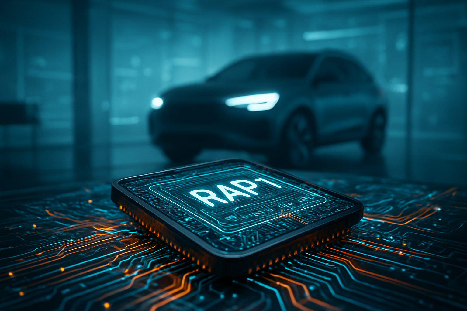
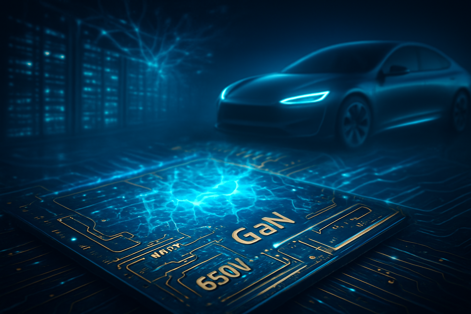
    In a move that signals a tectonic shift in the semiconductor landscape, power electronics giant onsemi (NASDAQ: ON) and contract manufacturing leader GlobalFoundries (NASDAQ: GFS) have announced a strategic partnership to develop and mass-produce 650V Gallium Nitride (GaN) power devices. Announced in late December 2025, this collaboration is designed to tackle the two most pressing energy challenges of 2026: the insatiable power demands of AI-driven data centers and the need for higher efficiency in the rapidly maturing electric vehicle (EV) market.

    The partnership represents a significant leap forward for wide-bandgap (WBG) materials, which are quickly replacing traditional silicon in high-performance applications. By combining onsemi's deep expertise in power systems and packaging with GlobalFoundries’ high-volume, U.S.-based manufacturing capabilities, the two companies aim to provide a resilient and scalable supply of GaN chips. As of January 7, 2026, the industry is already seeing the first ripples of this announcement, with customer sampling scheduled to begin in the first half of this year.

    The technical core of this partnership centers on a 200mm (8-inch) enhancement-mode (eMode) GaN-on-silicon manufacturing process. Historically, GaN production was limited to 150mm wafers, which constrained volume and kept costs high. The transition to 200mm wafers at GlobalFoundries' Malta, New York, facility allows for significantly higher yields and better cost-efficiency, effectively moving GaN from a niche, premium material to a mainstream industrial standard. The 650V rating is particularly strategic, as it serves as the "sweet spot" for devices that interface with standard electrical grids and the 400V battery architectures currently dominant in the automotive sector.

    Unlike traditional silicon transistors, which struggle with heat and efficiency at high frequencies, these 650V GaN devices can switch at much higher speeds with minimal energy loss. This capability allows engineers to use smaller passive components, such as inductors and capacitors, leading to a dramatic reduction in the overall size and weight of power supplies. Furthermore, onsemi is integrating these GaN FETs with its proprietary silicon drivers and controllers in a "system-in-package" (SiP) architecture. This integration reduces electromagnetic interference (EMI) and simplifies the design process for engineers, who previously had to manually tune discrete components from multiple vendors.

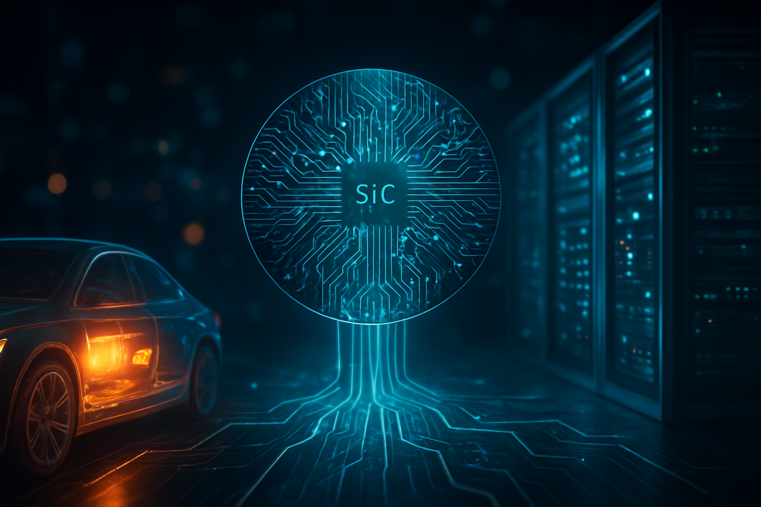
    Initial reactions from the semiconductor research community have been overwhelmingly positive. Analysts note that while Silicon Carbide (SiC) has dominated the high-voltage (1200V+) EV traction inverter market, GaN is proving to be the superior choice for the 650V range. Dr. Aris Silvestros, a leading power electronics researcher, commented that the "integration of gate drivers directly with GaN transistors on a 200mm line is the 'holy grail' for power density, finally breaking the thermal barriers that have plagued high-performance computing for years."

    For the broader tech industry, the implications are profound. AI giants and data center operators stand to be the biggest beneficiaries. As Large Language Models (LLMs) continue to scale, the power density of server racks has become a critical bottleneck. Traditional silicon-based power units are no longer sufficient to feed the latest AI accelerators. The onsemi-GlobalFoundries partnership enables the creation of 12kW power modules that fit into the same physical footprint as older 3kW units. This effectively quadruples the power density of data centers, allowing companies like NVIDIA (NASDAQ: NVDA) and Microsoft (NASDAQ: MSFT) to pack more compute power into existing facilities without requiring massive infrastructure overhauls.

    In the automotive sector, the partnership puts pressure on established players like Wolfspeed (NYSE: WOLF) and STMicroelectronics (NYSE: STM). While these competitors have focused heavily on Silicon Carbide, the onsemi-GF alliance's focus on 650V GaN targets the high-volume "onboard charger" (OBC) and DC-DC converter markets. By making these components smaller and more efficient, automakers can reduce vehicle weight and extend range—or conversely, use smaller, cheaper batteries to achieve the same range. The bidirectional capability of these GaN devices also facilitates "Vehicle-to-Grid" (V2G) technology, allowing EVs to act as mobile batteries for the home or the electrical grid, a feature that is becoming a standard requirement in 2026 model-year vehicles.

    Strategically, the partnership provides a major "Made in America" advantage. By utilizing GlobalFoundries' New York fabrication plants, onsemi can offer its customers a supply chain that is insulated from geopolitical tensions in East Asia. This is a critical selling point for U.S. and European automakers and government-linked data center projects that are increasingly prioritized by domestic content requirements and supply chain security.

    The broader significance of this development lies in the global "AI Power Crisis." As of early 2026, data centers are projected to consume over 1,000 Terawatt-hours of electricity annually. The efficiency gains offered by GaN—reducing heat loss by up to 50% compared to silicon—are no longer just a cost-saving measure; they are a prerequisite for the continued growth of artificial intelligence. If the world is to meet its sustainability goals while expanding AI capabilities, the transition to wide-bandgap materials like GaN is non-negotiable.

    This milestone also marks the end of the "Silicon Era" for high-performance power conversion. Much like the transition from vacuum tubes to transistors in the mid-20th century, the shift from Silicon to GaN and SiC represents a fundamental change in how we manage electrons. The partnership between onsemi and GlobalFoundries is a signal that the manufacturing hurdles that once held GaN back have been cleared. This mirrors previous AI milestones, such as the shift to GPU-accelerated computing; it is an enabling technology that allows the software and AI models to reach their full potential.

    However, the rapid transition is not without concerns. The industry must now address the "talent gap" in power electronics engineering. Designing with GaN requires a different mindset than designing with Silicon, as the high switching speeds can create complex signal integrity issues. Furthermore, while the U.S.-based manufacturing is a boon for security, the global industry must ensure that the raw material supply of Gallium remains stable, as it is often a byproduct of aluminum and zinc mining and is subject to its own set of geopolitical sensitivities.

    Looking ahead, the roadmap for 650V GaN is just the beginning. Experts predict that the success of this partnership will lead to even higher levels of integration, where the power stage and the logic stage are combined on a single chip. This would enable "smart" power systems that can autonomously optimize their efficiency in real-time based on the workload of the AI processor they are feeding. In the near term, we expect to see the first GaN-powered AI server racks hitting the market by late 2026, followed by a wave of 2027 model-year EVs featuring integrated GaN onboard chargers.

    Another horizon for this technology is the expansion into consumer electronics and 5G/6G infrastructure. While 650V is the current focus, the lessons learned from this high-volume 200mm process will likely be applied to lower-voltage GaN for smartphones and laptops, leading to even smaller "brickless" chargers. In the long term, we may see GaN-based power conversion integrated directly into the cooling systems of supercomputers, further blurring the line between electrical and thermal management.

    The primary challenge remaining is the standardization of GaN testing and reliability protocols. Unlike silicon, which has decades of reliability data, GaN is still building its long-term track record. The industry will be watching closely as the first large-scale deployments of the onsemi-GF chips go live this year to see if they hold up to the rigorous 10-to-15-year lifespans required by the automotive and industrial sectors.

    The partnership between onsemi and GlobalFoundries is more than just a business deal; it is a foundational pillar for the next phase of the technological revolution. By scaling 650V GaN to high-volume production, these two companies are providing the "energy backbone" required for both the AI-driven digital world and the electrified physical world. The key takeaways are clear: GaN has arrived as a mainstream technology, U.S. manufacturing is reclaiming a central role in the semiconductor supply chain, and the "power wall" that threatened to stall AI progress is finally being dismantled.

    As we move through 2026, this development will be remembered as the moment when the industry stopped talking about the potential of wide-bandgap materials and started delivering them at the scale the world requires. The long-term impact will be measured in gigawatts of energy saved and miles of EV range gained. For investors and tech enthusiasts alike, the coming weeks and months will be a critical period to watch for the first performance benchmarks from the H1 2026 sampling phase, which will ultimately prove if GaN can live up to its promise as the fuel for the future.


    This content is intended for informational purposes only and represents analysis of current AI developments.

    TokenRing AI delivers enterprise-grade solutions for multi-agent AI workflow orchestration, AI-powered development tools, and seamless remote collaboration platforms.
    For more information, visit https://www.tokenring.ai/.

  • The Wide-Bandgap Tipping Point: How GaN and SiC Are Breaking the Energy Wall for AI and EVs

    The Wide-Bandgap Tipping Point: How GaN and SiC Are Breaking the Energy Wall for AI and EVs

    As of January 6, 2026, the semiconductor industry has officially entered the "Wide-Bandgap (WBG) Era." For decades, traditional silicon was the undisputed king of power electronics, but the dual pressures of the global electric vehicle (EV) transition and the insatiable power hunger of generative AI have pushed silicon to its physical limits. In its place, Gallium Nitride (GaN) and Silicon Carbide (SiC) have emerged as the foundational materials for a new generation of high-efficiency, high-density power systems that are effectively "breaking the energy wall."

    The immediate significance of this shift cannot be overstated. With AI data centers now consuming more electricity than entire mid-sized nations and EV owners demanding charging times comparable to a gas station stop, the efficiency gains provided by WBG semiconductors are no longer a luxury—they are a requirement for survival. By allowing power systems to run hotter, faster, and with significantly less energy loss, GaN and SiC are enabling the next phase of the digital and green revolutions, fundamentally altering the economics of energy consumption across the globe.

    Technically, the transition to WBG materials represents a leap in physics. Unlike traditional silicon, which has a narrow "bandgap" (the energy required to move electrons into a conductive state), GaN and SiC possess much wider bandgaps—3.2 electron volts (eV) for SiC and 3.4 eV for GaN, compared to silicon’s 1.1 eV. This allows these materials to withstand much higher voltages and temperatures. In 2026, the industry has seen a massive move toward "Vertical GaN" (vGaN), a breakthrough that allows GaN to handle the 1200V+ requirements of heavy machinery and long-haul trucking, a domain previously reserved for SiC.

    The most significant manufacturing milestone of the past year was the shipment of the first 300mm (12-inch) GaN-on-Silicon wafers by Infineon Technologies AG (OTC: IFNNY). This transition from 200mm to 300mm wafers has nearly tripled the chip yield per wafer, bringing GaN closer to cost parity with legacy silicon than ever before. Meanwhile, SiC technology has matured through the adoption of "trench" architectures, which increase current density and reduce resistance, allowing for even smaller and more efficient traction inverters in EVs.

    These advancements differ from previous approaches by focusing on "system-level" efficiency rather than just component performance. In the AI sector, this has manifested as "Power-on-Package," where GaN power converters are integrated directly onto the processor substrate. This eliminates the "last inch" of power delivery losses that previously plagued high-performance computing. Initial reactions from the research community have been overwhelmingly positive, with experts noting that these materials have effectively extended the life of Moore’s Law by solving the thermal throttling issues that threatened to stall AI hardware progress.

    The competitive landscape for power semiconductors has been radically reshaped. STMicroelectronics (NYSE: STM) has solidified its leadership in the EV space through its fully integrated SiC production facility in Italy, securing long-term supply agreements with major European and American automakers. onsemi (NASDAQ: ON) has similarly positioned itself as a critical partner for the industrial and energy sectors with its EliteSiC M3e platform, which has set new benchmarks for reliability in harsh environments.

    In the AI infrastructure market, Navitas Semiconductor (NASDAQ: NVTS) has emerged as a powerhouse, partnering with NVIDIA (NASDAQ: NVDA) to provide the 12kW power supply units (PSUs) required for the latest "Vera Rubin" AI architectures. These PSUs achieve 98% efficiency, meeting the rigorous 80 PLUS Titanium standard and allowing data center operators to pack more compute power into existing rack footprints. This has created a strategic advantage for companies like Vertiv Holdings Co (NYSE: VRT), which integrates these WBG-based power modules into their liquid-cooled data center solutions.

    The disruption to existing products is profound. Legacy silicon-based Insulated-Gate Bipolar Transistors (IGBTs) are being rapidly phased out of the high-end EV market. Even Tesla (NASDAQ: TSLA), which famously announced a plan to reduce SiC usage in 2023, has pivoted toward a "hybrid" approach in its mass-market platforms—using high-efficiency SiC for performance-critical components while optimizing die area to manage costs. This shift has forced traditional silicon suppliers to either pivot to WBG or face obsolescence in the high-growth power sectors.

    The wider significance of the WBG revolution lies in its impact on global sustainability and the "Energy Wall." As AI models grow in complexity, the energy required to train and run them has become a primary bottleneck. WBG semiconductors act as a pressure valve, reducing the cooling requirements and energy waste in data centers by up to 40%. This is not just a technical win; it is a geopolitical necessity as governments around the world implement stricter energy consumption mandates for digital infrastructure.

    In the transportation sector, the move to 800V architectures powered by SiC has effectively solved "range anxiety" for many consumers. By enabling 15-minute ultra-fast charging and extending vehicle range by 7-10% through efficiency alone, WBG materials have done more to accelerate EV adoption than almost any battery chemistry breakthrough in the last five years. This transition is comparable to the shift from vacuum tubes to transistors in the mid-20th century, marking a fundamental change in how humanity manages and converts electrical energy.

    However, the rapid transition has raised concerns regarding the supply chain. The "SiC War" of 2025, which saw a surge in demand outstrip supply, led to the dramatic restructuring of Wolfspeed (NYSE: WOLF). After successfully emerging from a mid-2025 financial reorganization, Wolfspeed is now a leaner, 200mm-focused player, highlighting the immense capital intensity and risk involved in scaling these advanced materials. There are also environmental concerns regarding the energy-intensive process of growing SiC crystals, though these are largely offset by the energy saved during the chips' lifetime.

    Looking ahead, the next frontier for WBG semiconductors is the integration of diamond-based materials. While still in the early experimental phases in 2026, "Ultra-Wide-Bandgap" (UWBG) materials like diamond and Gallium Oxide ($Ga_2O_3$) promise thermal conductivity and voltage handling that dwarf even GaN and SiC. In the near term, we expect to see GaN move into the main traction inverters of entry-level EVs, further driving down costs and making high-efficiency electric mobility accessible to the masses.

    Experts predict that by 2028, we will see the first "All-GaN" data centers, where every stage of power conversion—from the grid to the chip—is handled by WBG materials. This would represent a near-total decoupling of compute growth from energy growth. Another area to watch is the integration of WBG into renewable energy grids; SiC-based string inverters are expected to become the standard for utility-scale solar and wind farms, drastically reducing the cost of transmitting green energy over long distances.

    The rise of Gallium Nitride and Silicon Carbide marks a pivotal moment in the history of technology. By overcoming the thermal and electrical limitations of silicon, these materials have provided the "missing link" for the AI and EV revolutions. The key takeaways from the start of 2026 are clear: efficiency is the new currency of the tech industry, and the ability to manage power at scale is the ultimate competitive advantage.

    As we look toward the rest of the decade, the significance of this development will only grow. The "Wide-Bandgap Tipping Point" has passed, and the industry is now in a race to scale. In the coming weeks and months, watch for more announcements regarding 300mm GaN production capacity and the first commercial deployments of Vertical GaN in heavy industry. The era of silicon dominance in power is over; the era of WBG has truly begun.


    This content is intended for informational purposes only and represents analysis of current AI developments.

    TokenRing AI delivers enterprise-grade solutions for multi-agent AI workflow orchestration, AI-powered development tools, and seamless remote collaboration platforms.
    For more information, visit https://www.tokenring.ai/.

  • Rivian Declares Independence: Unveiling the RAP1 AI Chip to Replace NVIDIA in EVs

    Rivian Declares Independence: Unveiling the RAP1 AI Chip to Replace NVIDIA in EVs

    In a move that signals a paradigm shift for the electric vehicle (EV) industry, Rivian Automotive, Inc. (NASDAQ: RIVN) has officially declared its "silicon independence." During its inaugural Autonomy & AI Day on December 11, 2025, the company unveiled the Rivian Autonomy Processor 1 (RAP1), its first in-house AI chip designed specifically to power the next generation of self-driving vehicles. By developing its own custom silicon, Rivian joins an elite tier of technology-first automakers like Tesla, Inc. (NASDAQ: TSLA), moving away from the off-the-shelf hardware that has dominated the industry for years.

    The introduction of the RAP1 chip is more than just a hardware upgrade; it is a strategic maneuver to decouple Rivian’s future from the supply chains and profit margins of external chipmakers. The new processor will serve as the heart of Rivian’s third-generation Autonomous Computing Module (ACM3), replacing the NVIDIA Corporation (NASDAQ: NVDA) DRIVE Orin systems currently found in its second-generation R1T and R1S models. With this transition, Rivian aims to achieve a level of vertical integration that promises not only superior performance but also significantly improved unit economics as it scales production of its upcoming R2 and R3 vehicle platforms.

    Technical Specifications and the Leap to 1,600 TOPS

    The RAP1 is a technical powerhouse, manufactured on the cutting-edge 5nm process node by Taiwan Semiconductor Manufacturing Company (NYSE: TSM). While the previous NVIDIA-based system delivered approximately 500 Trillion Operations Per Second (TOPS), the new ACM3 module, powered by dual RAP1 chips, reaches a staggering 1,600 sparse TOPS. This represents a 4x leap in raw AI processing power, specifically optimized for the complex neural networks required for real-time spatial awareness. The chip architecture utilizes 14 Armv9 Cortex-A720AE cores and a proprietary "RivLink" low-latency interconnect, allowing the system to process over 5 billion pixels per second from the vehicle’s sensor suite.

    This custom architecture differs fundamentally from previous approaches by prioritizing "sparse" computing—a method that ignores irrelevant data in a scene to focus processing power on critical objects like pedestrians and moving vehicles. Unlike the more generalized NVIDIA DRIVE Orin, which is designed to be compatible with a wide range of manufacturers, the RAP1 is "application-specific," meaning every transistor is tuned for Rivian’s specific "Large Driving Model" (LDM). This foundation model utilizes Group-Relative Policy Optimization (GRPO) to distill driving strategies from millions of miles of real-world data, a technique that Rivian claims allows for more human-like decision-making in complex urban environments.

    Initial reactions from the AI research community have been overwhelmingly positive, with many experts noting that Rivian’s move toward custom silicon is the only viable path to achieving Level 4 autonomy. "General-purpose GPUs are excellent for development, but they carry 'silicon tax' in the form of unused features and higher power draw," noted one senior analyst at the Silicon Valley AI Summit. By stripping away the overhead of a multi-client chip like NVIDIA's, Rivian has reportedly reduced its compute-related Bill of Materials (BOM) by 30%, a crucial factor for the company’s path to profitability.

    Market Implications: A Challenge to NVIDIA and Tesla

    The competitive implications of the RAP1 announcement are far-reaching, particularly for NVIDIA. While NVIDIA remains the undisputed king of data center AI, Rivian’s departure highlights a growing trend of "silicon sovereignty" among high-end EV makers. As more manufacturers seek to differentiate through software, NVIDIA faces the risk of losing its foothold in the premium automotive edge-computing market. However, the blow is softened by the fact that Rivian continues to use thousands of NVIDIA H100 and H200 GPUs in its back-end data centers to train the very models that the RAP1 executes on the road.

    For Tesla, the RAP1 represents the first credible threat to its Full Self-Driving (FSD) hardware supremacy. Rivian is positioning its ACM3 as a more robust alternative to Tesla’s vision-only approach by re-integrating high-resolution LiDAR and imaging radar alongside its cameras. This "belt and suspenders" philosophy, powered by the massive throughput of the RAP1, aims to win over safety-conscious consumers who may be skeptical of pure-vision systems. Furthermore, Rivian’s $5.8 billion joint venture with Volkswagen Group (OTC: VWAGY) suggests that this custom silicon could eventually find its way into Porsche or Audi models, giving Rivian a massive strategic advantage as a hardware-and-software supplier to the broader industry.

    The Broader AI Landscape: Vertical Integration as the New Standard

    The emergence of the RAP1 fits into a broader global trend where the line between "car company" and "AI lab" is increasingly blurred. We are entering an era where the value of a vehicle is determined more by its silicon and software stack than by its motor or battery. Rivian’s move mirrors the "Apple-ification" of the automotive industry—a strategy pioneered by Apple Inc. (NASDAQ: AAPL) in the smartphone market—where controlling the hardware, the operating system, and the application layer results in a seamless, highly optimized user experience.

    However, this shift toward custom silicon is not without its risks. The development costs for a 5nm chip are astronomical, often exceeding hundreds of millions of dollars. By taking this in-house, Rivian is betting that its future volume, particularly with the R2 SUV, will be high enough to amortize these costs. There are also concerns regarding the "walled garden" effect; as automakers move to proprietary chips, the industry moves further away from standardization, potentially complicating future regulatory efforts to establish universal safety benchmarks for autonomous driving.

    Future Horizons: The Path to Level 4 Autonomy

    Looking ahead, the first real-world test for the RAP1 will come in late 2026 with the launch of the Rivian R2. This vehicle will be the first to ship with the ACM3 computer as standard equipment, targeting true Level 3 and eventually Level 4 "eyes-off" autonomy on mapped highways. In the near term, Rivian plans to launch an "Autonomy+" subscription service in early 2026, which will offer "Universal Hands-Free" driving to existing second-generation owners, though the full Level 4 capabilities will be reserved for the RAP1-powered Gen 3 hardware.

    The long-term potential for this technology extends beyond passenger vehicles. Experts predict that Rivian could license its ACM3 platform to other industries, such as autonomous delivery robotics or even maritime applications. The primary challenge remaining is the regulatory hurdle; while the hardware is now capable of Level 4 autonomy, the legal framework for "eyes-off" driving in the United States remains a patchwork of state-by-state approvals. Rivian will need to prove through billions of simulated and real-world miles that the RAP1-powered system is significantly safer than a human driver.

    Conclusion: A New Era for Rivian

    Rivian’s unveiling of the RAP1 AI chip marks a definitive moment in the company’s history, transforming it from a niche EV maker into a formidable player in the global AI landscape. By delivering 1,600 TOPS of performance and slashing costs by 30%, Rivian has demonstrated that it has the technical maturity to compete with both legacy tech giants and established automotive leaders. The move secures Rivian’s place in the "Silicon Club," alongside Tesla and Apple, as a company capable of defining its own technological destiny.

    As we move into 2026, the industry will be watching closely to see if the RAP1 can deliver on its promise of Level 4 autonomy. The success of this chip will likely determine the fate of the R2 platform and Rivian’s long-term viability as a profitable, independent automaker. For now, the message is clear: the future of the intelligent vehicle will not be bought off the shelf—it will be built from the silicon up.


    This content is intended for informational purposes only and represents analysis of current AI developments.

    TokenRing AI delivers enterprise-grade solutions for multi-agent AI workflow orchestration, AI-powered development tools, and seamless remote collaboration platforms.
    For more information, visit https://www.tokenring.ai/.

  • Powering the Intelligence Explosion: Navitas Semiconductor’s 800V Revolution Redefines AI Data Centers and Electric Mobility

    Powering the Intelligence Explosion: Navitas Semiconductor’s 800V Revolution Redefines AI Data Centers and Electric Mobility

    As the world grapples with the insatiable power demands of the generative AI era, Navitas Semiconductor (Nasdaq: NVTS) has emerged as a pivotal architect of the infrastructure required to sustain it. By spearheading a transition to 800V high-voltage architectures, the company is effectively dismantling the "energy wall" that threatened to stall the deployment of next-generation AI clusters and the mass adoption of ultra-fast-charging electric vehicles.

    This technological pivot marks a fundamental shift in how electricity is managed at the edge of compute and mobility. As of December 2025, the industry has moved beyond traditional silicon-based power systems, which are increasingly seen as the bottleneck in the race for AI supremacy. Navitas’s integrated approach, combining Gallium Nitride (GaN) and Silicon Carbide (SiC) technologies, is now the gold standard for efficiency, enabling the 120kW+ server racks and 18-minute EV charging cycles that define the current technological landscape.

    The 12kW Breakthrough: Engineering the "AI Factory"

    The technical cornerstone of this revolution is Navitas’s dual-engine strategy, which pairs its GaNSafe™ and GeneSiC™ platforms to achieve unprecedented power density. In May 2025, Navitas unveiled its 12kW power supply unit (PSU), a device roughly the size of a laptop charger that delivers enough energy to power an entire residential block. Utilizing the IntelliWeave™ digital control platform, these units achieve over 97% efficiency, a critical metric when every fraction of a percentage point in energy loss translates into millions of dollars in cooling costs for hyperscale data centers.

    This advancement is a radical departure from the 54V systems that dominated the industry just two years ago. At 54V, delivering the thousands of amps required by modern GPUs like NVIDIA’s (Nasdaq: NVDA) Blackwell and the new Rubin Ultra series resulted in massive "I²R" heat losses and required thick, heavy copper busbars. By moving to an 800V High-Voltage Direct Current (HVDC) architecture—codenamed "Kyber" in Navitas’s latest collaboration with NVIDIA—the system can deliver the same power with significantly lower current. This reduces copper wiring requirements by 45% and eliminates multiple energy-sapping AC-to-DC conversion stages, allowing for more compute density within the same physical footprint.

    Initial reactions from the AI research community have been overwhelmingly positive, with engineers noting that the 800V shift is as much a thermal management breakthrough as it is a power one. By integrating sub-350ns short-circuit protection directly into the GaNSafe chips, Navitas has also addressed the reliability concerns that previously plagued high-voltage wide-bandgap semiconductors, making them viable for the mission-critical "always-on" nature of AI factories.

    Market Positioning: The Pivot to High-Margin Infrastructure

    Navitas’s strategic trajectory throughout 2025 has seen the company aggressively pivot away from low-margin consumer electronics toward the high-stakes sectors of AI, EV, and solar energy. This "Navitas 2.0" strategy has positioned the company as a direct challenger to legacy giants like Infineon Technologies (OTC: IFNNY) and STMicroelectronics (NYSE: STM). While STMicroelectronics continues to hold a strong grip on the Tesla (Nasdaq: TSLA) supply chain, Navitas has carved out a leadership position in the burgeoning 800V AI data center market, which is projected to reach $2.6 billion by 2030.

    The primary beneficiaries of this development are the "Magnificent Seven" tech giants and specialized AI cloud providers. For companies like Microsoft (Nasdaq: MSFT) and Alphabet (Nasdaq: GOOGL), the adoption of Navitas’s 800V technology allows them to pack more GPUs into existing data center shells, deferring billions in capital expenditure for new facility construction. Furthermore, Navitas’s recent partnership with Cyient Semiconductors to build a GaN ecosystem in India suggests a strategic move to diversify the global supply chain, providing a hedge against geopolitical tensions that have historically impacted the semiconductor industry.

    Competitive implications are stark: traditional silicon power chipmakers are finding themselves sidelined in the high-performance tier. As AI chips exceed the 1,000W-per-GPU threshold, the physical properties of silicon simply cannot handle the heat and switching speeds required. This has forced a consolidation in the industry, with companies like Wolfspeed (NYSE: WOLF) and Texas Instruments (Nasdaq: TXN) racing to scale their own 200mm SiC and GaN production lines to match Navitas's specialized "pure-play" efficiency.

    The Wider Significance: Breaking the Energy Wall

    The 800V revolution is more than just a hardware upgrade; it is a necessary evolution in the face of a global energy crisis. As AI compute demand is expected to consume up to 10% of global electricity by 2030, the efficiency gains provided by wide-bandgap materials like GaN and SiC have become a matter of environmental and economic survival. Navitas’s technology directly addresses the "Energy Wall," a point where the cost and heat of power delivery would theoretically cap the growth of AI intelligence.

    Comparisons are being drawn to the transition from vacuum tubes to transistors in the mid-20th century. Just as the transistor allowed for the miniaturization and proliferation of computers, 800V power semiconductors are allowing for the "physicalization" of AI—moving it from massive, centralized warehouses into more compact, efficient, and even mobile forms. However, this shift also raises concerns about the concentration of power (both literal and figurative) within the few companies that control the high-efficiency semiconductor supply chain.

    Sustainability advocates have noted that while the 800V shift saves energy, the sheer scale of AI expansion may still lead to a net increase in carbon emissions. Nevertheless, the ability to reduce copper usage by hundreds of kilograms per rack and improve EV range by 10% through GeneSiC traction inverters represents a significant step toward a more resource-efficient future. The 800V architecture is now the bridge between the digital intelligence of AI and the physical reality of the power grid.

    Future Horizons: From 800V to Grid-Scale Intelligence

    Looking ahead to 2026 and beyond, the industry expects Navitas to push the boundaries even further. The recent announcement of a 2300V/3300V Ultra-High Voltage (UHV) SiC portfolio suggests that the company is looking past the data center and toward the electrical grid itself. These devices could enable solid-state transformers and grid-scale energy storage systems that are smaller and more efficient than current infrastructure, potentially integrating renewable energy sources directly into AI data centers.

    In the near term, the focus remains on the "Rubin Ultra" generation of AI chips. Navitas has already unveiled 100V GaN FETs optimized for the point-of-load power boards that sit directly next to these processors. The challenge will be scaling production to meet the explosive demand while maintaining the rigorous quality standards required for automotive and hyperscale applications. Experts predict that the next frontier will be "Vertical Power Delivery," where power semiconductors are mounted directly beneath the AI chip to further reduce path resistance and maximize performance.

    A New Era of Power Electronics

    Navitas Semiconductor’s 800V revolution represents a definitive chapter in the history of AI development. By solving the physical constraints of power delivery, they have provided the "oxygen" for the AI fire to continue burning. The transition from silicon to GaN and SiC is no longer a future prospect—it is the present reality of 2025, driven by the dual engines of high-performance compute and the electrification of transport.

    The significance of this development cannot be overstated: without the efficiency gains of 800V architectures, the current trajectory of AI scaling would be economically and physically impossible. In the coming weeks and months, industry watchers should look for the first production-scale deployments of the 12kW "Kyber" racks and the expansion of GaNSafe technology into mainstream, affordable electric vehicles. Navitas has successfully positioned itself not just as a component supplier, but as a fundamental enabler of the 21st-century technological stack.


    This content is intended for informational purposes only and represents analysis of current AI developments.

    TokenRing AI delivers enterprise-grade solutions for multi-agent AI workflow orchestration, AI-powered development tools, and seamless remote collaboration platforms.
    For more information, visit https://www.tokenring.ai/.

  • Powering the Future: onsemi Navigates a Pivotal Shift in the EV and Industrial Semiconductor Landscape

    Powering the Future: onsemi Navigates a Pivotal Shift in the EV and Industrial Semiconductor Landscape

    As of December 19, 2025, ON Semiconductor (NASDAQ: ON), commonly known as onsemi, finds itself at a critical juncture in the global semiconductor market. After navigating a challenging 2024 and a transitional 2025, the company is emerging as a stabilizing leader in the power semiconductor space. While the broader automotive and industrial sectors have faced a prolonged "inventory digestion" phase, onsemi's strategic pivot toward high-growth AI data center power solutions and its aggressive vertical integration in Silicon Carbide (SiC) have caught the attention of Wall Street analysts.

    The immediate significance of onsemi’s current position lies in its resilience. Despite a cyclical downturn that saw revenue contract year-over-year, the company has maintained steady gross margins in the high 30% range and recently authorized a massive $6 billion share repurchase program. This move, combined with a flurry of analyst price target adjustments, signals a growing confidence that the company has reached its "trough" and is poised for a significant recovery as it scales its next-generation 200mm SiC manufacturing capabilities.

    Technical Milestones and the 200mm SiC Transition

    The technical narrative for onsemi in late 2025 is dominated by the transition from 150mm to 200mm (8-inch) Silicon Carbide wafers. This shift is not merely a change in size but a fundamental leap in manufacturing efficiency and cost-competitiveness. By moving to larger wafers, onsemi expects to significantly increase the number of chips per wafer, effectively lowering the cost of high-voltage power semiconductors essential for 800V electric vehicle (EV) architectures. The company has confirmed it is on track to begin generating meaningful revenue from 200mm production in early 2026, a milestone that industry experts view as a prerequisite for maintaining its roughly 24% share of the global SiC market.

    In addition to SiC, onsemi has made significant strides in its Field Stop 7 (FS7) IGBT technology. These devices are designed for high-power industrial applications, including solar inverters and energy storage systems. The FS7 platform offers lower switching losses and higher power density compared to previous generations, allowing for more compact and efficient energy infrastructure. Initial reactions from the industrial research community have been positive, noting that these advancements are crucial for the global transition toward renewable energy grids that require robust, high-efficiency power management.

    Furthermore, onsemi’s "Fab Right" strategy—a multi-year effort to consolidate manufacturing into fewer, more efficient, vertically integrated sites—is beginning to pay technical dividends. By controlling the entire supply chain from substrate growth to final module assembly, the company has achieved a level of quality control and supply assurance that few competitors can match. This vertical integration is particularly critical in the SiC market, where material scarcity and processing complexity have historically been major bottlenecks.

    Competitive Dynamics and the AI Data Center Pivot

    While the EV market has seen a slower-than-expected recovery in North America and Europe throughout 2025, onsemi has successfully offset this weakness by aggressively entering the AI data center market. In a landmark collaboration announced earlier this year with NVIDIA (NASDAQ: NVDA), onsemi is now supporting 800VDC power architectures for next-generation AI server racks. These high-voltage systems are designed to minimize energy loss as power moves from the grid to the GPU, a critical factor for data centers that are increasingly constrained by power availability and cooling costs.

    This pivot has placed onsemi in direct competition with other power giants like STMicroelectronics (NYSE: STM) and Infineon Technologies (OTCMKTS: IFNNY). While STMicroelectronics currently leads the SiC market by a small margin, onsemi’s recent deal with GlobalFoundries (NASDAQ: GFS) to develop 650V Gallium Nitride (GaN) power devices suggests a broadening of its portfolio. GaN technology is particularly suited for the ultra-compact power supply units (PSUs) used in AI servers, providing a complementary offering to its high-voltage SiC products.

    The competitive landscape is also being reshaped by onsemi’s focus on the Chinese EV market. Despite geopolitical tensions, onsemi has secured several major design wins with leading Chinese OEMs who are leading the charge in 800V vehicle adoption. By positioning itself as a key supplier for the most technologically advanced vehicles, onsemi is creating a strategic moat that protects its market share against lower-cost competitors who lack the high-voltage expertise and integrated supply chain of the Arizona-based firm.

    Wider Significance for the AI and Energy Landscape

    The evolution of onsemi reflects a broader trend in the technology sector: the convergence of AI and energy efficiency. As AI models become more computationally intensive, the demand for sophisticated power management has shifted from a niche industrial concern to a primary driver of the semiconductor industry. onsemi’s ability to double its AI-related revenue year-over-year in 2025 highlights how critical power semiconductors have become to the "AI Gold Rush." Without the efficiency gains provided by SiC and GaN, the energy requirements of modern data centers would be unsustainable.

    This development also underscores the changing nature of the EV market. The "hype phase" of 2021-2023 has given way to a more mature, performance-oriented market where efficiency is the primary differentiator. onsemi’s focus on 800V systems aligns with the industry’s shift toward faster charging and longer range, proving that the underlying technology is still advancing even if consumer adoption rates have hit a temporary plateau.

    However, the path forward is not without concerns. Analysts have pointed to the risks of overcapacity as onsemi, Wolfspeed (NYSE: WOLF), and others all race to bring massive SiC manufacturing hubs online. The Czech Republic hub and the expansion in Korea represent multi-billion-dollar bets that demand will eventually catch up with supply. If the EV recovery stalls further or if AI power needs are met by alternative technologies, these capital-intensive investments could pressure the company’s balance sheet in the late 2020s.

    Future Developments and Market Outlook

    Looking ahead to 2026 and beyond, the primary catalyst for onsemi will be the full-scale ramp of its 200mm SiC production. This transition is expected to unlock a new level of profitability, allowing the company to compete more aggressively on price while maintaining its premium margins. Experts predict that as the cost of SiC modules drops, we will see a "trickle-down" effect where high-efficiency power electronics move from luxury EVs and high-end AI servers into mid-range consumer vehicles and broader industrial automation.

    Another area to watch is the expansion of the onsemi-GlobalFoundries partnership. The integration of GaN technology into onsemi’s "EliteSiC" ecosystem could create a "one-stop shop" for power management, covering everything from low-power consumer electronics to megawatt-scale industrial grids. Challenges remain, particularly in the yield rates of 200mm SiC and the continued geopolitical complexities of the semiconductor supply chain, but onsemi’s diversified approach across AI, automotive, and industrial sectors provides a robust buffer.

    In the near term, the market will be closely watching onsemi’s Q4 2025 earnings report and its initial guidance for 2026. If the company can demonstrate that its AI revenue continues to scale while its automotive business stabilizes, the consensus price target of $59.00 may prove to be conservative. Many analysts believe that as the "inventory digestion" cycle ends, onsemi could see a rapid re-rating of its stock price, potentially reaching the $80-$85 range as investors price in the 2026 recovery.

    Summary of the Power Semiconductor Landscape

    In conclusion, ON Semiconductor has successfully navigated one of the most volatile periods in recent semiconductor history. By maintaining financial discipline through its $6 billion buyback program and "Fab Right" strategy, the company has prepared itself for the next leg of growth. The shift from a purely automotive-focused story to a diversified power leader serving the AI data center market is a significant milestone that redefines onsemi’s role in the tech ecosystem.

    As we move into 2026, the key takeaways for investors and industry observers are the company’s technical leadership in the 200mm SiC transition and its critical role in enabling the energy-efficient AI infrastructure of the future. While risks regarding global demand and manufacturing yields persist, onsemi’s strategic positioning makes it a bellwether for the broader health of the power semiconductor market. In the coming weeks, all eyes will be on the company’s execution of its manufacturing roadmap, which will ultimately determine its ability to lead the next generation of energy-efficient technology.


    This content is intended for informational purposes only and represents analysis of current AI and semiconductor developments.

    TokenRing AI delivers enterprise-grade solutions for multi-agent AI workflow orchestration, AI-powered development tools, and seamless remote collaboration platforms.
    For more information, visit https://www.tokenring.ai/.

  • Rivian and Volkswagen Forge AI-Powered Future with Groundbreaking SDV Platform

    Rivian and Volkswagen Forge AI-Powered Future with Groundbreaking SDV Platform

    Palo Alto, CA & Wolfsburg, Germany – November 20, 2025 – In a landmark collaboration set to redefine the automotive landscape, electric vehicle innovator Rivian Automotive, Inc. (NASDAQ: RIVN) and global automotive giant Volkswagen AG (XTRA: VOW3) have joined forces to develop a cutting-edge software-defined vehicle (SDV) platform. This strategic alliance, formalized as Rivian and Volkswagen Group Technologies (RV Tech), an equally owned joint venture established in November 2024, is poised to accelerate the integration of advanced AI and machine learning into future vehicles, promising a new era of intelligent mobility and setting a potential industry standard for automotive software. With Volkswagen committing up to $5.8 billion to the venture, the partnership signals a profound shift in how vehicles are designed, built, and experienced, emphasizing a software-first approach that prioritizes continuous innovation and enhanced user capabilities.

    The immediate significance of this collaboration is multi-faceted. For Rivian, the substantial financial injection provides crucial capital for its growth, including the ramp-up of its highly anticipated R2 line. It also validates Rivian's pioneering electrical architecture and software, extending its reach far beyond its own brand. For Volkswagen, the partnership offers a vital shortcut in its race to develop advanced SDVs, addressing previous challenges with in-house software development and positioning it to compete more effectively with tech-forward EV leaders. The broader automotive industry sees this as a clear indicator of the necessity for traditional automakers to embrace external expertise and collaboration to navigate the complex, software-driven future of mobility, with the potential for RV Tech to license its platform to other manufacturers.

    The Technical Backbone: Zonal Architecture and Unified AI

    At the heart of the Rivian-Volkswagen SDV platform lies a state-of-the-art zonal electronic architecture. This design represents a radical departure from traditional automotive electrical/electronic (E/E) architectures, which typically rely on a fragmented network of numerous Electronic Control Units (ECUs) each managing specific functions. Instead, RV Tech’s approach consolidates computing power into powerful, modular central computers that control all vehicle functions within defined zones. Rivian's second-generation (Gen 2) architecture, which forms the basis for this collaboration, aims to reduce the number of in-house developed ECUs from 17 to just seven, a significant decrease compared to the 60+ found in equivalent traditional electric cars. This consolidation drastically simplifies vehicle wiring, potentially cutting harness length by 1.6 miles and reducing weight by 44 pounds per vehicle, leading to a projected 40% cost reduction in the electrical Bill of Materials (BOM).

    The software technology underpinning this platform is built on a software-first philosophy, where a unified software stack runs across all vehicle systems. This integrated approach, leveraging AI and machine learning, is foundational for advanced capabilities such as highly automated driving features and sophisticated infotainment systems. Crucially, the platform supports continuous over-the-air (OTA) updates, allowing for ongoing feature enhancements, performance optimization, and the seamless deployment of new AI-driven functionalities throughout the vehicle’s lifecycle. This differs significantly from previous approaches where software updates were often tied to hardware cycles or required dealership visits. Initial reactions from industry experts have lauded the strategic benefits for Volkswagen, enabling it to "lift-and-shift a ready-made architecture" and accelerate its transition to a pure zonal design, thereby avoiding significant in-house development hurdles. However, some reports from late 2025 indicate integration challenges, with tensions arising from adapting Rivian's EV-centric software stack to Volkswagen's diverse portfolio, potentially delaying some Audi, Porsche, and Volkswagen model launches.

    The RV Tech joint venture has rapidly expanded its international engineering team to over 1,500 employees across the USA, Canada, Sweden, Serbia, and a newly established hub in Berlin, fostering a global approach to SDV development. Since spring 2025, RV Tech has successfully defined the hardware and electronic architecture specifications for reference vehicles from Volkswagen, Audi, and Scout brands. Development work on engineering prototypes commenced in summer 2025 at RV Tech facilities in Palo Alto and Irvine, California, with rigorous winter validation testing scheduled to begin in Q1 2026. This technical foundation is expected to be integrated into Rivian's R2, R3, and R3X product lines, with the R2 slated for launch in the first half of 2026, and the Volkswagen ID.EVERY1 set to be the first production vehicle to feature this SDV architecture in 2027.

    Reshaping the AI and Automotive Landscape

    The Rivian-Volkswagen SDV collaboration carries profound implications for AI companies, tech giants, and startups alike. Companies specializing in robust and scalable AI infrastructure, particularly cloud providers like Amazon Web Services (NASDAQ: AMZN), which Rivian already utilizes, and data management platforms such as Databricks, stand to benefit significantly from the increased demand for underlying computational power and data processing. The joint venture's ambition to create a "standard technology stack" for the wider automotive industry, potentially offering its co-developed electrical architecture and software for licensing, could create new market opportunities for AI companies capable of developing specialized, modular applications that integrate seamlessly with RV Tech's platform. This includes niche solutions for advanced sensor fusion, edge AI optimization, or specific in-car experiences.

    Conversely, AI companies and startups attempting to build entire automotive software stacks or proprietary autonomous driving systems will face heightened competition from RV Tech's well-funded and globally scalable solution. Major tech giants like Alphabet (NASDAQ: GOOGL) (with Android Automotive OS and Waymo) and Microsoft (NASDAQ: MSFT) (with Azure) will also find a formidable competitor in RV Tech, as it aims to become a foundational software layer for vehicles. If successful, this could limit the market share for alternative proprietary automotive software solutions. The collaboration also poses a significant disruption to traditional Tier 1 automotive suppliers, who have historically provided discrete ECUs and fragmented software. These suppliers will need to pivot rapidly towards offering holistic software modules, advanced sensors, or specialized processing units compatible with zonal SDV architectures.

    The partnership also intensifies pressure on other Original Equipment Manufacturers (OEMs), underscoring the challenges of developing complex automotive software in-house. Volkswagen's strategic shift to partner with Rivian, following struggles with its own software arm, Cariad, could serve as a blueprint for other automakers to pursue similar alliances or accelerate their internal AI and software initiatives. By combining Rivian's agile software expertise with Volkswagen's manufacturing might, RV Tech directly challenges EV leaders like Tesla, which, while having its own proprietary stack, is noted to lag in pure zonal architecture integration. The explicit intention to license the SDV platform to other automakers, and potentially even for internal combustion engine (ICE) vehicles, could establish RV Tech as a foundational technology provider, generating new, high-margin revenue and potentially setting a de facto industry standard for automotive software and AI integration, akin to Android in the mobile sector.

    Broader Significance and the AI Evolution

    The Rivian-Volkswagen SDV collaboration is a powerful testament to the broader AI landscape's evolution and its profound impact on the automotive sector. This partnership firmly places the SDV at the center of future mobility, transforming vehicles into dynamic, AI-powered platforms capable of continuous learning and improvement. The emphasis on in-vehicle intelligence, driven by the zonal architecture and powerful central computing, is foundational for developing advanced automated driving features, predictive maintenance, and highly personalized user experiences. This aligns with the global trend predicting that most vehicles will be AI-powered and software-defined by 2035, with the market for AI in automotive projected to exceed $850 billion by 2030.

    This current phase of automotive AI, exemplified by RV Tech, represents a significant leap from earlier milestones. Initial AI applications in vehicles were confined to simpler tasks like engine management or basic ADAS features, relying on rule-based systems. The last decade saw the proliferation of more sophisticated ADAS, leveraging sensors and AI for real-time hazard detection, and enhanced infotainment systems with voice recognition. However, the SDV paradigm shifts AI from being an additive feature to being an integral part of the vehicle's core operating system. This enables holistic "digital driving experiences" that evolve post-purchase through continuous OTA updates, moving beyond siloed AI applications to a foundational transformation of the vehicle's intelligence. Unlike AI breakthroughs in controlled environments, automotive AI operates in dynamic, real-world scenarios with critical safety implications, demanding exceptionally high levels of reliability and ethical consideration in its development.

    Despite the immense promise, the collaboration faces potential concerns. Reports from late 2025 highlight "turbulence" within the joint venture, citing integration difficulties and potential delays for several Volkswagen Group models. Tensions over software customization versus standardization, with Rivian favoring a streamlined system and VW brands seeking more flexibility, pose significant challenges. The adaptation of Rivian's EV-centric software for Volkswagen's diverse portfolio, potentially including ICE vehicles, also presents a complex technical hurdle. Furthermore, ensuring robust cybersecurity and data privacy will be paramount as vehicles become more interconnected and reliant on AI. Nevertheless, the strategic importance of this collaboration in accelerating Volkswagen's SDV capabilities and solidifying Rivian's technological leadership underscores its transformative potential.

    Future Horizons and Expert Predictions

    In the near term, the Rivian-Volkswagen SDV collaboration is set to hit critical milestones. Following the finalization of hardware specifications in spring 2025 and the commencement of engineering prototype development in summer 2025, rigorous winter validation testing of reference vehicles (from Volkswagen, Audi, and Scout brands) is scheduled for Q1 2026. This testing will be crucial for evaluating the SDV architecture's real-world performance under extreme conditions. Rivian's R2 midsize SUV, slated for launch in the first half of 2026, will be an early demonstration of the joint venture's advancements, with Rivian planning to integrate RV Tech's technologies across its R2, R3, and R3X product lines. The Volkswagen ID.EVERY1 is expected to be the first production vehicle from the Volkswagen Group to feature the SDV architecture, with a mass production launch targeted for 2027.

    Looking further ahead, Volkswagen Group intends to sequentially integrate the joint SDV architecture into its next-generation electric vehicles built on the Scalable Systems Platform (SSP). The ambitious long-term goal is to deploy this architecture across an impressive 30 million units by 2030, covering a wide range of segments, price points, and international markets. Potential applications and use cases on the horizon include increasingly sophisticated autonomous driving capabilities, highly personalized and responsive infotainment systems, and advanced predictive maintenance features that leverage AI to anticipate and address issues before they arise. The SDV platform's modularity and OTA capabilities mean vehicles will continuously improve throughout their lifespan, offering new features and enhanced performance to consumers.

    However, several challenges need to be addressed for the collaboration to fully realize its potential. The reported software integration difficulties and cultural differences between Rivian's agile startup culture and Volkswagen's more traditional corporate structure require careful navigation. Experts predict that while the partnership is a vital step for Volkswagen to overcome its legacy software issues and accelerate its SDV transition, the full benefits may take several years to materialize. The ability to effectively standardize key software components while allowing for brand-specific customization will be a delicate balancing act. Nevertheless, analysts widely agree that this collaboration will significantly hasten Volkswagen's SDV capabilities, simplify the implementation of autonomy and AI functions, and lead to substantial cost savings through reduced wiring and ECU counts.

    A New Chapter in AI-Driven Mobility

    The Rivian-Volkswagen SDV collaboration represents a pivotal moment in the history of automotive AI, signaling a definitive shift towards software-defined, AI-powered vehicles as the industry standard. The key takeaways from this venture are the strategic importance of combining agile software expertise with global manufacturing scale, the transformative potential of zonal electronic architectures, and the critical role of continuous OTA updates in delivering an evolving user experience. This partnership is not merely about building better cars; it's about creating intelligent, adaptable mobility platforms that can continuously learn, improve, and offer new functionalities throughout their lifecycle.

    The significance of this development in AI history within the automotive sector cannot be overstated. It underscores the recognition by even the most established automakers that software, AI, and data are now the primary differentiators, moving beyond traditional hardware and engineering prowess. The long-term impact is expected to be transformative, leading to more efficient vehicle development, substantial cost reductions, and an enhanced, personalized driving experience for consumers. Should RV Tech succeed in licensing its platform to other automakers, it could establish a de facto industry standard, profoundly influencing the trajectory of automotive software and AI integration for decades to come.

    In the coming weeks and months, all eyes will be on the Q1 2026 winter testing of the reference vehicles, which will provide crucial insights into the SDV architecture's real-world performance. The launch of Rivian's R2 vehicles in the first half of 2026 will also offer an early glimpse of the joint venture's technological advancements in a production vehicle. Furthermore, it will be critical to monitor how the reported integration challenges and "turbulence" within the joint venture are addressed, and whether any strategic adjustments are made to ensure the timely delivery of Volkswagen Group's upcoming SDV models. The success of this collaboration will not only shape the future of Rivian and Volkswagen but will also serve as a powerful barometer for the entire automotive industry's ability to embrace and leverage the full potential of artificial intelligence.


    This content is intended for informational purposes only and represents analysis of current AI developments.

    TokenRing AI delivers enterprise-grade solutions for multi-agent AI workflow orchestration, AI-powered development tools, and seamless remote collaboration platforms.
    For more information, visit https://www.tokenring.ai/.

  • The Unseen Architects: How Contract Semiconductor Manufacturing Powers the AI, EV, and 5G Revolution

    The Unseen Architects: How Contract Semiconductor Manufacturing Powers the AI, EV, and 5G Revolution

    In the intricate tapestry of modern technology, an often-overlooked yet utterly indispensable force is at play: Contract Semiconductor Manufacturing (CMO). These specialized foundries, acting as the silent titans of the industry, have become the crucial backbone enabling the explosive growth and relentless innovation across Artificial Intelligence (AI), Electric Vehicles (EVs), and 5G connectivity. By decoupling the monumental costs and complexities of chip fabrication from the ingenious act of chip design, CMOs have democratized access to cutting-edge manufacturing capabilities, fundamentally reshaping the global chip supply chain and accelerating the pace of technological advancement.

    The immediate significance of CMO lies in its transformative impact on innovation, scalability, and market growth. It empowers a new generation of "fabless" companies – from nimble AI startups to established tech giants like NVIDIA (NASDAQ: NVDA) and Qualcomm (NASDAQ: QCOM) – to pour their resources into groundbreaking research and development, focusing solely on designing the next generation of intelligent processors, efficient power management units, and high-speed communication chips. This strategic division of labor not only fosters unparalleled creativity but also ensures that the most advanced process technologies, often costing tens of billions of dollars to develop and maintain, are accessible to a wider array of innovators, propelling entire industries forward at an unprecedented rate.

    The Foundry Model: Precision Engineering at Hyperscale

    The core of Contract Semiconductor Manufacturing's technical prowess lies in its hyper-specialization. Foundries like Taiwan Semiconductor Manufacturing Company (TSMC) (TPE: 2330), Samsung Foundry (KRX: 005930), and GlobalFoundries (NASDAQ: GFS) dedicate their entire existence to the art and science of chip fabrication. This singular focus allows them to invest astronomical sums into state-of-the-art facilities, known as fabs, equipped with the most advanced lithography tools, such as Extreme Ultraviolet (EUV) technology, capable of etching features as small as 3 nanometers. These capabilities are far beyond the financial and operational reach of most individual design companies, making CMOs the gatekeepers of leading-edge semiconductor production.

    Technically, CMOs differ from traditional Integrated Device Manufacturers (IDMs) like Intel (NASDAQ: INTC) by not designing their own chips for market sale. Instead, they provide manufacturing services based on client designs. This model has led to the rapid adoption of advanced process nodes, crucial for the performance demands of AI, EVs, and 5G. For instance, the intricate neural network architectures that power generative AI models require billions of transistors packed into a tiny area, demanding the highest precision manufacturing. Similarly, the robust and efficient power semiconductors for EVs, often utilizing Gallium Nitride (GaN) and Silicon Carbide (SiC) wafers, are perfected and scaled within these foundries. For 5G infrastructure and devices, CMOs provide the necessary capacity for high-frequency, high-performance chips that are vital for massive data throughput and low latency.

    The technical specifications and capabilities offered by CMOs are continuously evolving. They are at the forefront of developing new packaging technologies, such as 3D stacking and chiplet architectures, which allow for greater integration and performance density, especially critical for AI accelerators and high-performance computing (HPC). The initial reaction from the AI research community and industry experts has been overwhelmingly positive, recognizing that without the foundry model, the sheer complexity and cost of manufacturing would severely bottleneck innovation. Experts frequently highlight the collaborative co-development of process technologies between fabless companies and foundries as a key driver of current breakthroughs, ensuring designs are optimized for the manufacturing process from conception.

    Reshaping the Competitive Landscape: Beneficiaries and Disruptors

    The contract semiconductor manufacturing model has profoundly reshaped the competitive landscape across the tech industry, creating clear beneficiaries, intensifying competition, and driving strategic shifts. Fabless companies are the primary beneficiaries, as they can bring highly complex and specialized chips to market without the crippling capital expenditure of building and maintaining a fabrication plant. This allows companies like NVIDIA to dominate the AI chip market with their powerful GPUs, AMD (NASDAQ: AMD) to compete effectively in CPUs and GPUs, and a plethora of startups to innovate in niche AI hardware, autonomous driving processors, and specialized 5G components.

    For tech giants, the CMO model offers flexibility and strategic advantage. Companies like Apple (NASDAQ: AAPL) leverage foundries to produce their custom-designed A-series and M-series chips, giving them unparalleled control over hardware-software integration and performance. This allows them to differentiate their products significantly from competitors. The competitive implications are stark: companies that effectively partner with leading foundries gain a significant edge in performance, power efficiency, and time-to-market. Conversely, companies still heavily reliant on in-house manufacturing, like Intel, have faced immense pressure to adapt, leading to multi-billion dollar investments in new fabs and a strategic pivot to offering foundry services themselves.

    Potential disruption to existing products and services is constant. As CMOs push the boundaries of process technology, new chip designs emerge that can render older hardware obsolete faster, driving demand for upgrades in everything from data centers to consumer electronics. This dynamic environment encourages continuous innovation but also puts pressure on companies to stay at the leading edge. Market positioning is heavily influenced by access to the latest process nodes and reliable manufacturing capacity. Strategic advantages are gained not just through superior design, but also through strong, long-term relationships with leading foundries, ensuring preferential access to limited capacity and advanced technologies, which can be a critical differentiator in times of high demand or supply chain disruptions.

    Broader Significance: The Digital Economy's Foundation

    Contract Semiconductor Manufacturing's wider significance extends far beyond individual companies, underpinning the entire global digital economy and fitting squarely into broader AI and technology trends. It represents a fundamental shift towards horizontal specialization in the tech industry, where different entities excel in their core competencies – design, manufacturing, assembly, and testing. This specialization has not only driven efficiency but has also accelerated the pace of technological progress across the board. The impact is evident in the rapid advancements we see in AI, where increasingly complex models demand ever more powerful and efficient processing units; in EVs, where sophisticated power electronics and autonomous driving chips are crucial; and in 5G, where high-performance radio frequency (RF) and baseband chips enable ubiquitous, high-speed connectivity.

    The impact of CMOs is felt in virtually every aspect of modern life. They enable the smartphones in our pockets, the cloud servers that power our digital services, the medical devices that save lives, and the advanced defense systems that protect nations. Without the scalable, high-precision manufacturing provided by foundries, the vision of a fully connected, AI-driven, and electrified future would remain largely theoretical. However, this concentration of manufacturing power, particularly in a few key regions like East Asia, also raises potential concerns regarding geopolitical stability and supply chain resilience, as highlighted by recent global chip shortages.

    Compared to previous AI milestones, such as the development of deep learning or the AlphaGo victory, the role of CMOs is less about a single breakthrough and more about providing the foundational infrastructure that enables all subsequent breakthroughs. It's the silent enabler, the "invisible giant" that translates theoretical designs into tangible, functional hardware. This model has lowered the entry barriers for innovation, allowing a diverse ecosystem of companies to flourish, which in turn fuels further advancements. The global semiconductor market, projected to reach $1.1 trillion by 2029, with the foundry market alone exceeding $200 billion by 2030, is a testament to the indispensable role of CMOs in this exponential growth, driven largely by AI-centric architectures, IoT, and EV semiconductors.

    The Road Ahead: Future Developments and Challenges

    The future of Contract Semiconductor Manufacturing is intrinsically linked to the relentless march of technological progress in AI, EVs, and 5G. Near-term developments will likely focus on pushing the boundaries of process nodes further, with 2nm and even 1.4nm technologies on the horizon, promising even greater transistor density and performance. We can expect continued advancements in specialized packaging solutions like High Bandwidth Memory (HBM) integration and advanced fan-out packaging, crucial for the next generation of AI accelerators that demand massive data throughput. The development of novel materials beyond silicon, such as next-generation GaN and SiC for power electronics and new materials for photonics and quantum computing, will also be a key area of focus for foundries.

    Long-term, the industry faces challenges in sustaining Moore's Law, the historical trend of doubling transistor density every two years. This will necessitate exploring entirely new computing paradigms, such as neuromorphic computing and quantum computing, which will, in turn, require foundries to adapt their manufacturing processes to entirely new architectures and materials. Potential applications are vast, ranging from fully autonomous robotic systems and hyper-personalized AI assistants to smart cities powered by ubiquitous 5G and a fully electric transportation ecosystem.

    However, significant challenges need to be addressed. The escalating cost of developing and building new fabs, now routinely in the tens of billions of dollars, poses a substantial hurdle. Geopolitical tensions and the desire for greater supply chain resilience are driving efforts to diversify manufacturing geographically, with governments investing heavily in domestic semiconductor production. Experts predict a continued arms race in R&D and capital expenditure among leading foundries, alongside increasing strategic partnerships between fabless companies and their manufacturing partners to secure capacity and co-develop future technologies. The demand for highly skilled talent in semiconductor engineering and manufacturing will also intensify, requiring significant investment in education and workforce development.

    A Cornerstone of the Digital Age: Wrapping Up

    In summary, Contract Semiconductor Manufacturing stands as an undisputed cornerstone of the modern digital age, an "invisible giant" whose profound impact is felt across the entire technology landscape. Its model of specialized, high-volume, and cutting-edge fabrication has been instrumental in enabling the rapid innovation and scalable production required by the burgeoning fields of AI, Electric Vehicles, and 5G. By allowing chip designers to focus on their core competencies and providing access to prohibitively expensive manufacturing capabilities, CMOs have significantly lowered barriers to entry, fostered a vibrant ecosystem of innovation, and become the indispensable backbone of the global chip supply chain.

    The significance of this development in AI history, and indeed in the broader history of technology, cannot be overstated. It represents a paradigm shift that has accelerated the pace of progress, making possible the complex, powerful, and efficient chips that drive our increasingly intelligent and connected world. Without the foundry model, many of the AI breakthroughs we celebrate today, the widespread adoption of EVs, and the rollout of 5G networks would simply not be economically or technically feasible on their current scale.

    In the coming weeks and months, we should watch for continued announcements regarding new process node developments from leading foundries, government initiatives aimed at bolstering domestic semiconductor manufacturing, and strategic partnerships between chip designers and manufacturers. The ongoing race for technological supremacy will largely be fought in the advanced fabs of contract manufacturers, making their evolution and expansion critical indicators for the future trajectory of AI, EVs, 5G, and indeed, the entire global economy.


    This content is intended for informational purposes only and represents analysis of current AI developments.

    TokenRing AI delivers enterprise-grade solutions for multi-agent AI workflow orchestration, AI-powered development tools, and seamless remote collaboration platforms.
    For more information, visit https://www.tokenring.ai/.

  • Silicon Carbide Surges: Powering a Greener Future with a 12.5% CAGR to Reach $1.8 Billion by 2027

    Silicon Carbide Surges: Powering a Greener Future with a 12.5% CAGR to Reach $1.8 Billion by 2027

    The global Silicon Carbide (SiC) market is experiencing an unprecedented surge, poised to reach a staggering US$1,810.56 million by 2027, growing at a robust Compound Annual Growth Rate (CAGR) of 12.5%. This rapid expansion is not merely a market trend but a fundamental shift in power electronics, driven primarily by the insatiable demands of the electric vehicle (EV) revolution and the accelerating transition to renewable energy sources. SiC, with its superior material properties, is proving to be the indispensable backbone for next-generation energy-efficient technologies, fundamentally reshaping how power is managed and delivered across industries.

    This significant growth reflects a pivotal moment where traditional silicon-based power electronics are reaching their inherent limitations. SiC, a wide-bandgap semiconductor, offers vastly improved efficiency, power density, and thermal performance, making it the material of choice for applications requiring high power, high voltage, and high-temperature operation. Its immediate significance lies in its ability to extend EV driving ranges, enable faster charging, and maximize the energy yield from solar and wind power, directly contributing to global decarbonization efforts and the broader adoption of sustainable technologies.

    The Technical Edge: Why SiC is the New Gold Standard

    The technical superiority of Silicon Carbide over conventional silicon is the bedrock of its market dominance. SiC boasts a bandgap of approximately 3.2 eV, nearly three times that of silicon (1.12 eV), allowing it to withstand significantly higher electric fields before breakdown. This translates to devices capable of operating at much higher voltages (up to 3.3 kV in commercial MOSFETs) with lower leakage currents and reduced on-resistance. Furthermore, SiC's exceptional thermal conductivity (100–400 W/m·K, more than three times silicon's) enables efficient heat dissipation, allowing devices to operate reliably at elevated temperatures (up to 250°C commercially) and at higher power densities, often negating the need for bulky cooling systems.

    These intrinsic properties yield profound differences in power electronics. SiC devices offer vastly faster switching speeds and lower switching and conduction losses, leading to significantly higher power conversion efficiencies—up to 80% reduction in power loss compared to silicon IGBTs. This efficiency directly translates to tangible benefits in critical applications. In Electric Vehicle (EV) traction inverters, SiC MOSFETs enhance power density and reduce energy loss, potentially increasing an EV's driving range by 5-10%. For instance, a SiC-based inverter can achieve 220 kW output power with a peak efficiency of 99.1%, while reducing weight by approximately 6 kg and volume by 30% compared to a Si IGBT-based solution. SiC is also crucial for the emerging 800V EV architectures, where it can reduce losses by up to 70% compared to silicon.

    For on-board chargers (OBCs), SiC's high switching frequency and low losses enable faster charging times and increased power density, allowing for smaller, lighter, and more compact charger designs with peak system efficiencies of up to 98%. In renewable energy systems, particularly solar inverters, SiC minimizes losses, leading to higher energy conversion efficiencies (often exceeding 98-99%) and enabling more compact, reliable designs. Its ability to handle higher voltages also allows solar farms to increase string voltage, reducing cable size and inverter count, thereby lowering overall project costs. Initial reactions from the research community and industry experts universally hail SiC as a "game-changer" and a "disruptive technology," noting its rapid adoption and continuous R&D efforts focused on improving wafer quality, reducing defects, and enhancing packaging technologies. Despite challenges like initial costs and manufacturing complexities, the long-term outlook remains overwhelmingly positive.

    Corporate Power Plays: Who Benefits from the SiC Boom

    The rapid expansion of the SiC market is creating a new hierarchy of beneficiaries, from material manufacturers to automotive giants and renewable energy innovators. Major SiC manufacturers are strategically positioning themselves for dominance. STMicroelectronics (NYSE: STM), for instance, holds the largest market share in SiC power devices and is investing heavily in a full-process SiC factory in Italy, expected by 2026, alongside an 8-inch SiC joint venture in China. Infineon Technologies AG (FWB: IFX) is expanding its SiC capabilities through product innovation and factory expansions, such as in Kulim, Malaysia. Wolfspeed, Inc. (NYSE: WOLF) stands out as a pioneer and the world's largest supplier of SiC materials, particularly for automotive-grade MOSFET substrates, leveraging a vertically integrated model and a first-mover advantage in 8-inch wafer technology. Onsemi (NASDAQ: ON) has rapidly ascended in market share, largely due to its EliteSiC series and a significant contract with Volkswagen for EV traction inverters. Other key players like ROHM Co., Ltd. (TYO: 6767), Fuji Electric Co., Ltd. (TYO: 6504), Toshiba Electronic Devices & Storage Corporation (TYO: 6502), and Microchip Technology Inc. (NASDAQ: MCHP) are also making substantial investments.

    In the automotive sector, Electric Vehicle (EV) manufacturers are the primary drivers of SiC demand, expected to account for 70% of SiC power device consumption by 2030. Early adopters like Tesla (NASDAQ: TSLA), which integrated SiC into its Model 3 in 2017, have paved the way. Now, major players such as Hyundai (KRX: 005380), Kia (KRX: 000270), BYD (HKG: 1211), Nio (NYSE: NIO), Xpeng (NYSE: XPEV), and Li Auto (NASDAQ: LI) are heavily utilizing SiC to enhance vehicle efficiency, range, and charging speeds. The Volkswagen Group (FWB: VOW) has secured a multi-year contract with Onsemi for EV traction inverters, signaling a broader industry shift. These OEMs are increasingly forming partnerships with SiC manufacturers to secure supply and co-develop optimized solutions.

    In the renewable energy sector, companies like Wolfspeed, Inc. are leading the charge in providing SiC power devices for solar inverters, wind turbines, and battery-based energy storage systems. SiC's ability to handle high power densities reduces energy losses in power conversion, critical for scaling green technologies and integrating smart grids. The competitive landscape is characterized by intense R&D, significant capital investments in manufacturing capacity, and a strategic push towards vertical integration to ensure supply chain control and cost efficiency. The transition to larger 8-inch SiC wafers is a crucial strategy to reduce device costs, with many players investing heavily in this shift. While challenges such as higher initial costs, material defects, and recent market adjustments due to a slowdown in EV demand persist, companies adopting SiC gain significant strategic advantages in efficiency, performance, and system miniaturization, ensuring their competitive edge in an increasingly electrified world.

    A Cornerstone of the Green Revolution: Wider Implications

    The expansion of the Silicon Carbide market is far more than an industrial success story; it represents a fundamental cornerstone of the global electrification and decarbonization trends, deeply embedded in the push for sustainable technology. Valued at approximately $2 billion today, the global SiC device market is projected to surge to between $11 billion and $14 billion by 2030, underscoring its pivotal role in transforming energy systems worldwide.

    SiC is a critical enabler for electrification, particularly in the automotive industry, where EVs are poised to account for 70% or more of future SiC power device demand. Its ability to increase EV range by over 20% with the same battery pack, reduce charging times to under 40 minutes for fast chargers, and enable high-efficiency 800V powertrains is indispensable for widespread EV adoption. Beyond vehicles, SiC is increasingly adopted in industrial automation, telecommunications (including 5G infrastructure), and data centers, where its high-frequency handling reduces energy consumption.

    In decarbonization efforts, SiC is a powerhouse. It is essential in renewable energy sources like solar panel cells and wind turbines, where it efficiently converts and manages large amounts of energy. SiC semiconductors offer potential energy savings of up to 30% compared to traditional silicon chips, significantly contributing to CO2 emission reduction. For data centers, which consume vast amounts of electricity, SiC devices generate less heat, improving energy efficiency and reducing the need for extensive cooling systems. If all global data centers replaced silicon components with SiC, the energy savings could power Manhattan for a year. This aligns perfectly with the broader trend towards sustainable technology, as SiC's superior material properties—including a bandgap nearly three times that of silicon, a 10-fold higher breakdown field strength, and three times better thermal conductivity—enable smaller, more robust, and more reliable electronic systems with a reduced environmental footprint.

    However, the rapid growth also brings potential concerns. High manufacturing costs, complex production processes, and the higher initial environmental impact of SiC wafer production compared to silicon are challenges that need addressing. Supply chain volatility, including a recent "capacity glut" and price erosion for SiC wafers, along with increased competition, demand continuous innovation. Material defects and technical integration issues also require ongoing R&D. Despite these hurdles, the transition from silicon to SiC is widely described as a "once-in-a-generation technological shift," echoing the transformative impact of the Insulated Gate Bipolar Transistor (IGBT) in the 1980s. SiC transistors are now poised to achieve similar, if not greater, impact by further eliminating losses and enabling unprecedented efficiency and miniaturization, where silicon has reached its physical limits. The interplay between SiC and other wide bandgap semiconductors like Gallium Nitride (GaN) further highlights this dynamic evolution in power electronics.

    The Road Ahead: SiC's Future Trajectory

    The future of Silicon Carbide technology is brimming with potential, promising continued advancements and an expanding sphere of influence far beyond its current strongholds in EVs and renewable energy. In the near term (1-3 years), the industry is intensely focused on the widespread transition to 200 mm (8-inch) SiC wafers. This shift, already being spearheaded by companies like Wolfspeed, Inc. (NYSE: WOLF), Infineon Technologies AG (FWB: IFX), and Robert Bosch GmbH (ETR: BOSCH), is critical for enhancing manufacturing efficiency, boosting yields, and significantly reducing costs. Broader deployment and mass production scaling of 200mm wafers are anticipated by 2026. Concurrently, efforts are concentrated on improving wafer quality to eliminate microstructural defects and advancing packaging technologies to fully exploit SiC's capabilities in harsh operating environments. New generations of SiC MOSFETs, promising even greater power density and switching efficiency, are expected to be introduced every 2 to 2.5 years.

    Looking further ahead (beyond 3 years), "radical innovations" in SiC technology are on the horizon, with companies like STMicroelectronics (NYSE: STM) hinting at breakthroughs by 2027. This could include integrated sensing functions within SiC devices, further diversifying their utility. Research into alternative SiC polytypes and the synergy of SiC manufacturing with AI and digital twin technologies are also expected to optimize production processes.

    Beyond its current applications, SiC is poised to revolutionize numerous other high-growth sectors. Its high-frequency and power-handling capabilities make it ideal for 5G and 6G infrastructure, enabling faster data transmission and robust connectivity. In data centers, SiC devices can drastically improve energy efficiency by reducing heat generation in power supplies, crucial for the demands of AI and high-performance computing. Industrial automation and motor drives will benefit from SiC's enhanced durability and efficiency, leading to reduced energy consumption in heavy machinery. Its extreme temperature resilience and radiation resistance position SiC as a key material for aerospace and defense components, including satellites and aircraft. Other emerging applications include railway systems, consumer electronics (for faster charging), medical devices (due to biocompatibility), MEMS, photonics devices, and smart grid infrastructure.

    Despite this promising outlook, challenges remain. The high cost of SiC wafers due to complex and lengthy production processes, along with difficulties arising from SiC's extreme hardness and brittleness during manufacturing, continue to be significant hurdles. Material defects and ensuring a robust, reliable supply chain at scale also require continuous attention. Experts, however, remain optimistic, predicting continued substantial market growth with CAGRs ranging from 10.7% to 25.7% through 2032. SiC is widely expected to soon surpass silicon as the dominant semiconductor for power devices with voltage ratings above 600V. While the automotive sector will remain a key driver, diversification into non-EV applications is essential. The industry will prioritize vertical integration and a relentless focus on cost reduction, particularly through the acceleration of 200mm wafer production, to solidify SiC's role as a critical enabler for a more electrified and sustainable future.

    A Transformative Era: The Lasting Impact of SiC

    The rapid expansion of the Silicon Carbide market marks a transformative era in power electronics, fundamentally reshaping industries and accelerating the global shift towards a sustainable future. The projected growth to US$1,810.56 million by 2027, driven by a 12.5% CAGR, is not just a statistical projection but a testament to SiC's undeniable technological superiority and its critical role in enabling the next generation of energy-efficient solutions.

    Key takeaways underscore SiC's indispensable contribution: its superior wide bandgap properties, high thermal conductivity, and faster switching speeds translate directly into higher efficiency, increased power density, and enhanced reliability across a spectrum of applications. This makes it the cornerstone for extending the range and accelerating the charging of Electric Vehicles, maximizing the energy yield from renewable sources like solar and wind, and revolutionizing power management in data centers, 5G infrastructure, and industrial automation. SiC is effectively breaking the performance barriers that traditional silicon has encountered, propelling industries into a new era of energy optimization.

    This development holds immense significance in AI history and the broader tech industry. While not an AI development itself, SiC's role in powering AI-driven data centers and advanced robotics highlights its foundational importance to the entire technological ecosystem. It represents a "once-in-a-generation technological shift," akin to previous semiconductor breakthroughs that laid the groundwork for entirely new capabilities. Its long-term impact will be profound, enabling a more electrified, efficient, and decarbonized world. By facilitating the development of smaller, lighter, and more powerful electronic systems, SiC is a crucial enabler for achieving global climate goals and fostering a truly sustainable technological landscape.

    In the coming weeks and months, market watchers should pay close attention to several key indicators. Continued investments in SiC production facilities, particularly the acceleration towards 200mm wafer manufacturing by major players like STMicroelectronics (NYSE: STM), Wolfspeed, Inc. (NYSE: WOLF), and Infineon Technologies AG (FWB: IFX), will be crucial for scaling supply and driving down costs. Strategic partnerships between SiC manufacturers and automotive OEMs will also define the competitive landscape. Furthermore, any new breakthroughs in material quality, defect reduction, or advanced packaging technologies will further unlock SiC's full potential. Despite short-term market fluctuations and competitive pressures, the Silicon Carbide market is poised for sustained, impactful growth, solidifying its legacy as a pivotal force in the global energy transition and the advancement of modern technology.


    This content is intended for informational purposes only and represents analysis of current AI developments.

    TokenRing AI delivers enterprise-grade solutions for multi-agent AI workflow orchestration, AI-powered development tools, and seamless remote collaboration platforms.
    For more information, visit https://www.tokenring.ai/.

  • Powering Progress: Analog and Industrial Semiconductors Drive the Next Wave of Innovation

    The foundational components of our increasingly intelligent and electrified world, analog and industrial semiconductors, are undergoing a profound transformation. Far from the spotlight often cast on advanced digital processors, these critical chips are quietly enabling revolutionary advancements across electric vehicles (EVs), artificial intelligence (AI) data centers, the Industrial Internet of Things (IIoT), and renewable energy systems. Recent breakthroughs in materials science, packaging technologies, and novel computing architectures are dramatically enhancing efficiency, power density, and embedded intelligence, setting new benchmarks for performance and sustainability. This continuous wave of innovation is not merely incremental; it is fundamental to unlocking the full potential of next-generation technologies and addressing pressing global challenges like energy consumption and computational demands.

    At the forefront of this evolution, companies like ON Semiconductor (NASDAQ: ON) are driving significant advancements. Their latest offerings, including cutting-edge wide-bandgap (WBG) materials like Silicon Carbide (SiC) and Gallium Nitride (GaN), alongside sophisticated power management and sensing solutions, are crucial for managing power, converting energy, and interpreting real-world data with unprecedented precision and efficiency. The immediate significance of these developments lies in their ability to dramatically reduce energy loss, shrink device footprints, and empower intelligence closer to the data source, thereby accelerating the deployment of sustainable and smart technologies across virtually every industry.

    Technical Deep Dive: SiC, GaN, and the Rise of Analog Intelligence

    The core of the current revolution in analog and industrial semiconductors lies in the strategic shift towards wide-bandgap (WBG) materials, primarily Silicon Carbide (SiC) and Gallium Nitride (GaN). These materials possess superior electrical properties compared to traditional silicon, allowing for operation at higher temperatures, voltages, and frequencies with significantly reduced energy losses and heat generation. This inherent advantage translates directly into more efficient power conversion, faster charging capabilities for EVs, and smaller, lighter power systems across industrial applications.

    Specific details of these advancements are impressive. ON Semiconductor (NASDAQ: ON), for instance, has introduced its M3e EliteSiC MOSFETs, 1200V SiC devices that leverage planar technology to achieve industry-leading specific on-resistance while maintaining robust short-circuit capability. This pushes the boundaries of power density and efficiency, crucial for high-power applications. Similarly, their new Field Stop 7 (FS7) IGBT technology, integrated into 1200V half-bridge QDual3 IGBT modules, boasts a 33% increase in current density. This allows for the design of smaller, lighter, and more cost-effective power systems for demanding applications such as central solar inverters, energy storage, and heavy-duty commercial vehicles. Beyond power, ON Semiconductor's Hyperlux SG image sensors and Hyperlux ID family are revolutionizing indirect Time-of-Flight (iToF) depth sensing, extending accurate distance measurements and providing precise depth data on moving objects, vital for advanced robotics and autonomous systems.

    A groundbreaking development from ON Semiconductor is their vertical GaN (vGaN) power semiconductors, built on novel GaN-on-GaN technology. Unlike traditional lateral GaN devices, vGaN conducts current vertically, setting new benchmarks for power density, efficiency, and ruggedness. This innovation can reduce energy loss by almost 50% and is particularly crucial for the demanding power requirements of AI data centers, EVs, renewable energy infrastructure, and industrial automation. This vertical architecture fundamentally differs from previous lateral approaches by enabling higher operating voltages and faster switching frequencies, overcoming some of the limitations of earlier GaN implementations and offering a direct path to higher performance and greater energy savings. The initial reactions from the industry and research community highlight the transformative potential of these WBG materials and vertical architectures, recognizing them as critical enablers for the next generation of high-power and high-frequency electronics.

    The emergence of novel analog computing architectures, such as Analog Machine Learning (AnalogML), further distinguishes this wave of innovation. Companies like Aspinity are pioneering AnalogML platforms for ultra-low-power edge devices, enabling real-time data processing directly at the sensor level. This drastically reduces the need for extensive digital computation and data transfer, extending battery life and reducing latency in wearables, smart home devices, and industrial sensors. Furthermore, research into new analog processors that perform calculations directly within physical circuits, bypassing energy-intensive data transfers, is showing promise. A notable development from Peking University claims an analog AI chip capable of outperforming high-end GPUs by up to 1,000 times for certain AI tasks, while consuming significantly less energy. This "software programmable analog processor" addresses previous challenges of precision and programmability in analog systems, offering a potentially revolutionary approach to AI model training and future communication networks like 6G. These analog approaches represent a significant departure from purely digital processing, offering inherent advantages in power efficiency and speed for specific computational tasks, particularly at the edge.

    Competitive Landscape and Market Dynamics

    The ongoing advancements in analog and industrial semiconductors are reshaping the competitive landscape, creating new opportunities and challenges for tech giants, specialized AI labs, and burgeoning startups. Companies that heavily invest in and successfully deploy wide-bandgap (WBG) materials, advanced packaging, and novel analog computing solutions stand to gain significant strategic advantages.

    Major players like ON Semiconductor (NASDAQ: ON), Infineon Technologies (ETR: IFX), STMicroelectronics (NYSE: STM), Texas Instruments (NASDAQ: TXN), and Analog Devices (NASDAQ: ADI) are poised to benefit immensely. ON Semiconductor, with its strong portfolio in SiC, vGaN, and sensing solutions, is particularly well-positioned to capitalize on the booming markets for EVs, AI data centers, and industrial automation. Their focus on high-efficiency power management and advanced sensing directly addresses critical needs in these high-growth sectors. Similarly, Infineon's investments in SiC and their collaboration with NVIDIA (NASDAQ: NVDA) on 800V DC power delivery for AI data centers highlight the strategic importance of these foundational technologies. Texas Instruments, a long-standing leader in analog, continues to expand its manufacturing capacity, particularly with new 300mm fabs, to meet the surging demand across industrial and automotive applications.

    This development also has significant competitive implications. Companies that lag in adopting WBG materials or fail to innovate in power management and sensor integration may find their products less competitive in terms of efficiency, size, and cost. The superior performance of SiC and GaN, for instance, can render older silicon-based power solutions less attractive for new designs, potentially disrupting established product lines. For AI labs and tech companies, access to highly efficient power management solutions and innovative analog computing architectures is crucial. The ability to power AI data centers with reduced energy consumption directly impacts operational costs and sustainability goals. Furthermore, the rise of AnalogML and edge AI, enabled by these semiconductors, could shift some processing away from centralized cloud infrastructure, potentially disrupting traditional cloud-centric AI models and empowering a new generation of intelligent edge devices.

    Market positioning is increasingly defined by a company's ability to offer integrated, high-performance, and energy-efficient solutions. Strategic partnerships, like Analog Devices' expanded collaboration with General Motors (NYSE: GM) for EV battery management systems, underscore the importance of deep industry integration. Companies that can provide comprehensive solutions, from power conversion to sensing and processing, will command a stronger position. The increasing complexity and specialization within the semiconductor industry also mean that startups focusing on niche areas, such as advanced analog computing for specific AI tasks or ultra-low-power edge processing, can carve out significant market shares by offering highly specialized and optimized solutions that complement the broader offerings of larger players.

    Wider Significance: Fueling the Intelligent and Electric Future

    The advancements in analog and industrial semiconductors represent more than just incremental improvements; they are foundational to the broader technological landscape and critical enablers for the most significant trends shaping our future. This wave of innovation fits perfectly into the overarching drive towards greater energy efficiency, pervasive intelligence, and sustainable electrification.

    The impact is far-reaching. In the context of the global energy transition, these semiconductors are indispensable. Wide-bandgap materials like SiC and GaN are directly contributing to the efficiency of electric vehicles, making them more practical and accessible by extending range and accelerating charging times. In renewable energy, they optimize power conversion in solar inverters and wind turbines, maximizing energy capture and integration into smart grids. For AI, the ability to power data centers with significantly reduced energy consumption is paramount, addressing a major environmental concern associated with the exponential growth of AI processing. Furthermore, the development of AnalogML and novel analog computing architectures is pushing intelligence to the very edge of networks, enabling real-time decision-making in IIoT devices and autonomous systems without relying on constant cloud connectivity, thereby enhancing responsiveness and data privacy.

    Potential concerns, however, include the complexity and cost associated with transitioning to new materials and manufacturing processes. The supply chain for SiC and GaN, while maturing, still faces challenges in scaling to meet exploding demand. Geopolitical tensions and the increasing strategic importance of semiconductor manufacturing also raise concerns about supply chain resilience and national security. Compared to previous AI milestones, where the focus was often on algorithmic breakthroughs or increases in computational power through traditional silicon, this current wave highlights the critical role of the underlying hardware infrastructure. It underscores that the future of AI is not solely about software; it is deeply intertwined with the physical limitations and capabilities of the chips that power it. These semiconductor innovations are as significant as past breakthroughs in processor architecture, as they unlock entirely new paradigms for power efficiency and localized intelligence, which are essential for the widespread deployment of AI in the real world.

    The Road Ahead: Anticipating Future Developments

    Looking ahead, the trajectory of analog and industrial semiconductors promises continued evolution and groundbreaking applications. Near-term developments are expected to focus on further refinements of wide-bandgap (WBG) materials, with ongoing research aimed at increasing voltage capabilities, reducing manufacturing costs, and improving the reliability and robustness of SiC and GaN devices. We can anticipate more integrated power modules that combine multiple WBG components into compact, highly efficient packages, simplifying design for engineers and accelerating adoption across industries.

    In the long term, the field will likely see a deeper convergence of analog and digital processing, especially at the edge. The promise of fully programmable analog AI chips, moving beyond specialized functions to more general-purpose analog computation, could revolutionize how AI models are trained and deployed, offering unprecedented energy efficiency for inference and even training directly on edge devices. Research into new materials beyond SiC and GaN, and novel device architectures that push the boundaries of quantum effects, may also emerge, offering even greater performance and efficiency gains.

    Potential applications and use cases on the horizon are vast. Beyond current applications, these advancements will enable truly autonomous systems that can operate for extended periods on minimal power, intelligent infrastructure that self-optimizes, and a new generation of medical devices that offer continuous, unobtrusive monitoring. The enhanced precision and reliability of industrial sensors, coupled with edge AI, will drive further automation and predictive maintenance in factories, smart cities, and critical infrastructure. Challenges that need to be addressed include the standardization of new manufacturing processes, the development of robust design tools for complex analog-digital hybrid systems, and the education of a workforce capable of designing and implementing these advanced technologies. Supply chain resilience will remain a critical focus, with continued investments in regional manufacturing capabilities.

    Experts predict that the relentless pursuit of energy efficiency and distributed intelligence will continue to be the primary drivers. The move towards "more than Moore" – integrating diverse functionalities beyond just logic – will see analog, power, and sensing capabilities increasingly co-packaged or integrated onto single chips. What experts predict will happen next is a continued acceleration in the adoption of SiC and GaN across all power-hungry applications, coupled with significant breakthroughs in analog computing that allow AI to become even more pervasive, efficient, and embedded into the fabric of our physical world.

    Comprehensive Wrap-Up: A Foundation for Future Innovation

    The current wave of innovation in analog and industrial semiconductors represents a pivotal moment in technological advancement. Key takeaways include the transformative power of wide-bandgap materials like Silicon Carbide and Gallium Nitride in achieving unprecedented energy efficiency and power density, the critical role of advanced packaging and vertical architectures in miniaturization and performance, and the emerging potential of novel analog computing to bring ultra-low-power intelligence to the edge. Companies such as ON Semiconductor (NASDAQ: ON) are not just participating in this shift; they are actively shaping it with their breakthrough technologies in power management, sensing, and material science.

    This development's significance in AI history, and indeed in the broader history of technology, cannot be overstated. It underscores that the advancements in AI are inextricably linked to the underlying hardware that powers them. Without these efficient and intelligent semiconductor foundations, the ambitious goals of widespread AI deployment, sustainable electrification, and pervasive connectivity would remain largely out of reach. These innovations are not merely supporting existing technologies; they are enabling entirely new paradigms of operation, making previously impossible applications feasible.

    Final thoughts on the long-term impact point to a future where technology is not only more powerful but also significantly more sustainable and integrated into our daily lives. Reduced energy consumption in data centers and EVs will have a tangible positive impact on climate change efforts, while distributed intelligence will lead to safer, more efficient, and more responsive autonomous systems and industrial operations. The continuous push for miniaturization and efficiency will also drive innovation in personal electronics, medical devices, and smart infrastructure, making technology more accessible and less intrusive.

    In the coming weeks and months, we should watch for continued announcements regarding new product launches utilizing SiC and GaN in automotive and industrial sectors, further investments in manufacturing capacity by key players, and the emergence of more concrete applications leveraging analog AI at the edge. The synergy between these semiconductor advancements and the rapidly evolving fields of AI, IoT, and electrification will undoubtedly continue to generate exciting and impactful developments that reshape our technological landscape.


    This content is intended for informational purposes only and represents analysis of current AI developments.

    TokenRing AI delivers enterprise-grade solutions for multi-agent AI workflow orchestration, AI-powered development tools, and seamless remote collaboration platforms.
    For more information, visit https://www.tokenring.ai/.

  • Silicon’s Crucial Ride: How Semiconductors are Redefining the Automotive Future

    Silicon’s Crucial Ride: How Semiconductors are Redefining the Automotive Future

    The automotive industry is in the midst of an unprecedented transformation, with semiconductors emerging as the undisputed architects of modern vehicle technology. As of November 2025, these critical components are driving a revolution in vehicle electrification, autonomous capabilities, connectivity, and intelligent user experiences. The immediate significance of chip advancements and stable supply chains cannot be overstated; they are the foundational elements enabling the next generation of smart, safe, and sustainable mobility. Recent events, including lingering supply chain vulnerabilities and geopolitical export constraints, underscore the industry's delicate reliance on these tiny powerhouses, pushing automakers and tech giants alike to prioritize resilient sourcing and cutting-edge chip development to secure the future of transportation.

    The Brains Behind the Wheel: Advanced AI Chips Drive Automotive Innovation

    The current wave of automotive AI chip advancements represents a significant leap from previous approaches, characterized by a move towards highly integrated, power-efficient, and specialized System-on-Chips (SoCs) and accelerators. This shift fundamentally redefines vehicle electronic architectures.

    NVIDIA (NASDAQ: NVDA), with its Drive Thor superchip, is unifying automated driving, parking, driver monitoring, and infotainment onto a single platform. Drive Thor boasts up to 2,000 teraflops (TOPS) of FP8 performance, a substantial increase from its predecessor, Drive Orin (254 TOPS). It integrates NVIDIA's Hopper Multi-Instance GPU architecture, Grace CPU, and a novel inference transformer engine, accelerating complex AI workloads. This architecture enables multi-domain computing, running multiple operating systems concurrently while maintaining ASIL D functional safety. Expected in 2025 models, Drive Thor signifies a consolidated, high-performance approach to vehicle intelligence.

    Qualcomm (NASDAQ: QCOM) is advancing its Snapdragon Ride Flex SoC family, designed to consolidate digital cockpit and ADAS functionalities. Flex SoCs in testing offer 16-24 TOPS for entry-level systems, with next-gen chips targeting up to 2000 TOPS for higher autonomy levels (L2+ to L4-5). These chips uniquely support mixed-criticality workloads on the same hardware, featuring a dedicated ASIL-D safety island and a pre-integrated software platform for multiple operating systems. Qualcomm's AI200 and AI250 accelerator cards, announced in October 2025, further enhance AI inference with innovative near-memory computing architectures, promising significant bandwidth and power efficiency improvements.

    Intel's (NASDAQ: INTC) Mobileye (NASDAQ: MBLY) continues its focus on vision-based ADAS and autonomous driving with the EyeQ Ultra. Built on a 5-nanometer process, it delivers 176 TOPS of AI acceleration, equivalent to ten EyeQ5s in a single package. This chip aims to provide full Level 4 autonomous driving from a single unit, utilizing proprietary accelerators like XNN and PMA cores for efficient deep learning. Intel's broader automotive initiatives, including the Adaptive Control Unit (ACU) U310 for EV powertrains and zonal controllers, and second-generation Intel Arc B-series Graphics for in-vehicle AI workloads, further cement its commitment. At Auto Shanghai 2025, Intel unveiled its second-generation AI-enhanced SDV SoC, noted as the industry's first multi-process node chiplet architecture.

    Tesla (NASDAQ: TSLA), known for its vertical integration, developed the custom D1 chip for its Dojo supercomputer, designed for training its Full Self-Driving (FSD) models. The D1 chip, manufactured by TSMC (NYSE: TSM) on a 7-nanometer process, features 50 billion transistors and delivers 376 teraflops at BF16 precision. Elon Musk also announced in November 2025 that Tesla completed the design review for its upcoming AI5 chip, claiming it will be 40 times more performant than its predecessor (AI4) and will be produced by both Samsung (KRX: 005930) and TSMC. This move signifies Tesla's aggressive pursuit of in-house silicon for both training and in-car hardware.

    These advancements differ significantly from previous approaches by emphasizing consolidation, specialized AI acceleration, and the use of advanced process nodes (e.g., 5nm, 7nm, with trends towards 3nm/4nm). The shift from distributed ECUs to centralized, software-defined vehicle (SDV) architectures reduces complexity and enables continuous over-the-air (OTA) updates. Initial reactions from the AI research community and industry experts highlight the convergence of automotive chip design with high-performance computing (HPC), the critical role of these chips in enabling SDVs, and the ongoing focus on efficiency and safety. However, concerns about high development costs, complex integration, cybersecurity, and supply chain resilience remain prominent.

    Corporate Chessboard: Navigating the Semiconductor Landscape

    The escalating role of semiconductors in automotive technology is profoundly reshaping the competitive landscape for AI companies, tech giants, and startups. The automotive semiconductor market is projected to exceed $67 billion by the end of 2025, with AI chips alone seeing a nearly 43% CAGR through 2034.

    Leading automotive semiconductor suppliers like Infineon (XTRA: IFX), NXP Semiconductors (NASDAQ: NXPI), STMicroelectronics (NYSE: STM), Texas Instruments (NASDAQ: TXN), and Renesas Electronics (TYO: 6723) are strong beneficiaries. They are investing heavily in next-generation microcontrollers, SoCs, and power semiconductors, particularly for EVs and ADAS. Infineon, for example, is expanding its Dresden plant and collaborating on Silicon Carbide (SiC) power semiconductor packages.

    High-performance AI chip innovators such as NVIDIA (NASDAQ: NVDA), Qualcomm (NASDAQ: QCOM), and AMD (NASDAQ: AMD) are key players. NVIDIA remains a dominant force in AI chips, while Qualcomm's Snapdragon Automotive platform gains significant traction. Foundries like TSMC (NYSE: TSM) and Samsung (KRX: 005930) are indispensable, with sub-16nm automotive capacity fully allocated through 2027, highlighting their critical role. Specialized power management companies like ON Semiconductor (NASDAQ: ON) also benefit from the demand for energy-efficient solutions for AI and EVs.

    The competitive implications are significant. Automakers are increasingly adopting vertical integration, designing chips in-house, challenging traditional Tier 1 and Tier 2 supplier models. This blurs the lines, transforming automakers into technology companies, as exemplified by Tesla (NASDAQ: TSLA) with its AI4 and AI5 chips, and Chinese OEMs like BYD (HKG: 1211) and Nio (NYSE: NIO). Strategic partnerships between carmakers, suppliers, and semiconductor companies are becoming essential for system-level compatibility and OTA updates. Geopolitical rivalry, with governments supporting domestic semiconductor ecosystems, further shapes supply chain decisions, leading to export controls and tariffs.

    Potential disruptions include the obsolescence of hardware-centric product development cycles by the rise of SDVs, which favor a software-first approach and continuous updates. Supply chain disruptions can still lead to delayed vehicle launches and feature rationalization. However, SDVs also open new revenue streams, such as subscription services for advanced features. As of November 2025, while the Nexperia crisis (a dispute involving a Dutch chipmaker owned by China's Wingtech Technology – SSE: 600745) appeared to be de-escalating due to a U.S.-China trade deal, the underlying geopolitical tensions and structural vulnerabilities in the semiconductor supply chain remain a defining characteristic of the market. Companies with diversified supply chains and proactive inventory management are better positioned to weather these disruptions.

    Beyond the Dashboard: Wider Societal and Ethical Implications

    The widespread integration of semiconductors and AI into the automotive industry extends far beyond vehicle performance, deeply impacting society, ethical considerations, and the broader AI landscape. This trend represents a critical phase in the "AI supercycle," where specialized AI chips for edge computing are becoming paramount.

    The automotive sector is a primary driver for edge AI, pushing the boundaries of chip design for real-time inference, low latency, and energy efficiency directly within the vehicle. This aligns with a broader AI trend of moving processing closer to the data source. AI is also revolutionizing automotive design, engineering, supply chains, and manufacturing, streamlining processes and reducing development cycles. The global automotive AI market is projected to grow from an estimated $4.71 billion in 2025 to approximately $48.59 billion by 2034, underscoring the pressing need for intelligent transport systems.

    Societal impacts are profound. Enhanced ADAS and autonomous driving are expected to significantly reduce accidents, leading to safer roads. Autonomous vehicles offer increased independence for individuals unable to drive, and the integration of 5G and V2X communication will support the development of smart cities. However, these advancements also bring potential concerns. Ethical AI presents challenges in programming moral dilemmas for autonomous vehicles in unavoidable accident scenarios, and addressing biases in algorithms is crucial to prevent discriminatory outcomes. The lack of transparency in complex AI algorithms raises questions about accountability, making explainable AI a necessity.

    Data privacy is another critical issue, as connected vehicles generate vast amounts of personal and behavioral data. Regulations like the EU Data Act are essential to ensure fair access and prevent data monopolies, but disparities in global regulations remain a challenge. Cybersecurity is paramount; the increasing connectivity and software-defined nature of vehicles create numerous attack surfaces. In 2024, the automotive and smart mobility ecosystem saw a sharp increase in cyber threats, with over 100 ransomware attacks. There is a strong push for embedded post-quantum cybersecurity to protect against future quantum computer attacks.

    Compared to previous AI milestones like Google's (NASDAQ: GOOGL) BERT (2018), OpenAI's GPT-3 (2020), and ChatGPT (2022), the current state of automotive AI in 2025 represents a move towards scaling AI capabilities, generating real value, and integrating AI into every aspect of operations. The EU AI Act (2024) established a regulatory framework for AI, directly influencing responsible AI development. By 2025, advanced reasoning-capable AI is entering full-scale production, leveraging fine-tuned large language models for domain-specific reasoning in complex decision support. This continuous innovation, powered by specialized semiconductors, creates a virtuous cycle of technological advancement that will continue to reshape the automotive industry and society.

    The Road Ahead: Future Developments and Predictions

    The trajectory of automotive semiconductors and AI points to a future where vehicles are not just transportation but sophisticated, evolving intelligent systems. The automotive semiconductor market is projected to double to $132 billion by 2030, with AI chips within this segment experiencing a CAGR of almost 43% through 2034.

    In the near term (2025-2030), expect the rapid rise of edge AI, with specialized processors like SoCs and NPUs enabling powerful, low-latency inference directly in the vehicle. Software-Defined Vehicles (SDVs) and zonal architectures will dominate, allowing for continuous over-the-air (OTA) updates and flexible functionalities. The widespread adoption of Wide-Bandgap (WBG) semiconductors like Silicon Carbide (SiC) and Gallium Nitride (GaN) will enhance EV efficiency and charging. Level 2 (L2) automation is mainstream, with mass deployment of Level 2+ and Level 3 (L3) vehicles being a key focus. The integration of 5G-capable chipsets will become essential for Vehicle-to-Everything (V2X) communication.

    Longer term (beyond 2030), expect continued advancements in AI chip architectures, emphasizing energy-efficient NPUs and neuromorphic computing for even more sophisticated in-vehicle AI. The push towards Level 4 (L4) and Level 5 (L5) autonomous driving will necessitate exponentially more powerful and reliable AI chips. SDVs are expected to account for 90% of total auto production by 2029 and dominate the market by 2040.

    Potential applications are vast, from advanced ADAS and fully autonomous driving (including robotaxi services) to hyper-personalized in-car experiences with AI-powered voice assistants and augmented reality. AI will optimize EV performance through intelligent battery management and enable predictive maintenance. V2X communication, manufacturing efficiency, and enhanced cybersecurity will also see significant AI integration.

    However, challenges remain. Supply chain resilience, cost optimization of cutting-edge AI chips, and the immense integration complexity of diverse hardware and software stacks are critical hurdles. Functional safety, reliability, and robust regulatory and ethical frameworks for autonomous vehicles and data privacy are paramount. The industry also faces talent shortages and the need for continuous innovation in energy-efficient AI processors and long-term software support.

    Experts predict the automotive semiconductor market to grow at a 10% CAGR to $132 billion by 2030, five times faster than the global automotive market. The average semiconductor content per vehicle will increase by 40% to over $1,400 by 2030. EV production is projected to exceed 40% of total vehicle production by 2030. There will be continued consolidation in the automotive AI chip market, with a few dominant players emerging, and significant investment in AI R&D by both car manufacturers and tech giants. The concept of Software-Defined Vehicles (SDVs) will fully mature, becoming the standard for personal and public transportation.

    The Intelligent Turn: A New Era for Automotive

    The journey of semiconductors in the automotive industry has evolved from humble beginnings to a central, indispensable role, powering the intelligence that defines modern vehicles. As of November 2025, this evolution marks a critical juncture in AI history, underscoring the profound impact of specialized silicon on real-world applications. The automotive AI chip market's explosive growth and the strategic shifts by industry players highlight a fundamental re-architecture of the vehicle itself, transforming it into a sophisticated, software-defined, and intelligent platform.

    The long-term impact will be nothing short of transformative: safer roads due to advanced ADAS, enhanced independence through autonomous driving, and hyper-personalized in-car experiences. Vehicles will become seamless extensions of our digital lives, constantly updated and optimized. However, this promising future is not without its complexities. The industry must navigate persistent supply chain vulnerabilities, the high cost of cutting-edge technology, and the ethical and regulatory quandaries posed by increasingly autonomous and data-rich vehicles. Cybersecurity, in particular, will remain a critical watchpoint as vehicles become more connected and susceptible to sophisticated threats.

    In the coming weeks and months, watch for continued advancements in chiplet technology and NPU integration, driving more sophisticated edge AI. Strategic collaborations between automakers and semiconductor companies will intensify, aimed at fortifying supply chains and co-developing flexible computing platforms. New product launches from major players will offer advanced real-time AI, sensor fusion, and connectivity solutions for SDVs. The adoption of 48V and 800V platforms for EVs will be a dominant trend, and the geopolitical landscape will continue to influence semiconductor supply chains. The full maturation of software-defined vehicles and the consolidation of domain controllers will emerge as significant growth drivers, reshaping how features are delivered and updated. The automotive industry, powered by sophisticated semiconductors and AI, is on the cusp of truly redefining the driving experience, promising a future that is safer, more efficient, and hyper-personalized.


    This content is intended for informational purposes only and represents analysis of current AI developments.

    TokenRing AI delivers enterprise-grade solutions for multi-agent AI workflow orchestration, AI-powered development tools, and seamless remote collaboration platforms.
    For more information, visit https://www.tokenring.ai/.