Tag: Foundry

  • Intel Officially Launches High-Volume Manufacturing for 18A Node, Fulfilling ‘5 Nodes in 4 Years’ Promise

    Intel Officially Launches High-Volume Manufacturing for 18A Node, Fulfilling ‘5 Nodes in 4 Years’ Promise

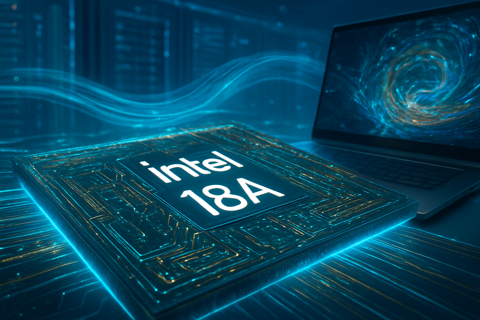
    Intel (NASDAQ: INTC) has officially entered the era of High-Volume Manufacturing (HVM) for its cutting-edge 1.8nm-class process node, known as Intel 18A. Announced on January 30, 2026, this milestone marks the formal completion of CEO Pat Gelsinger’s ambitious "5 Nodes in 4 Years" (5N4Y) strategy. By hitting this target, Intel has successfully transitioned through five distinct process generations—Intel 7, 4, 3, 20A, and 18A—in record time, effectively closing the technological gap that had allowed competitors to lead the semiconductor industry for nearly a decade.

    The launch is punctuated by the full-scale production of two flagship products: "Panther Lake," the next-generation Core Ultra consumer processor, and "Clearwater Forest," a high-efficiency Xeon server chip. With 18A now rolling off the lines at Fab 52 in Arizona, Intel has signaled to the world that it is once again a primary contender for the title of the world’s most advanced chip manufacturer, with yields currently estimated between 65% and 75%—a commercially viable range that rivals the early-stage ramp-ups of its toughest competitors.

    The Engineering Trifecta: RibbonFET, PowerVia, and the Death of FinFET

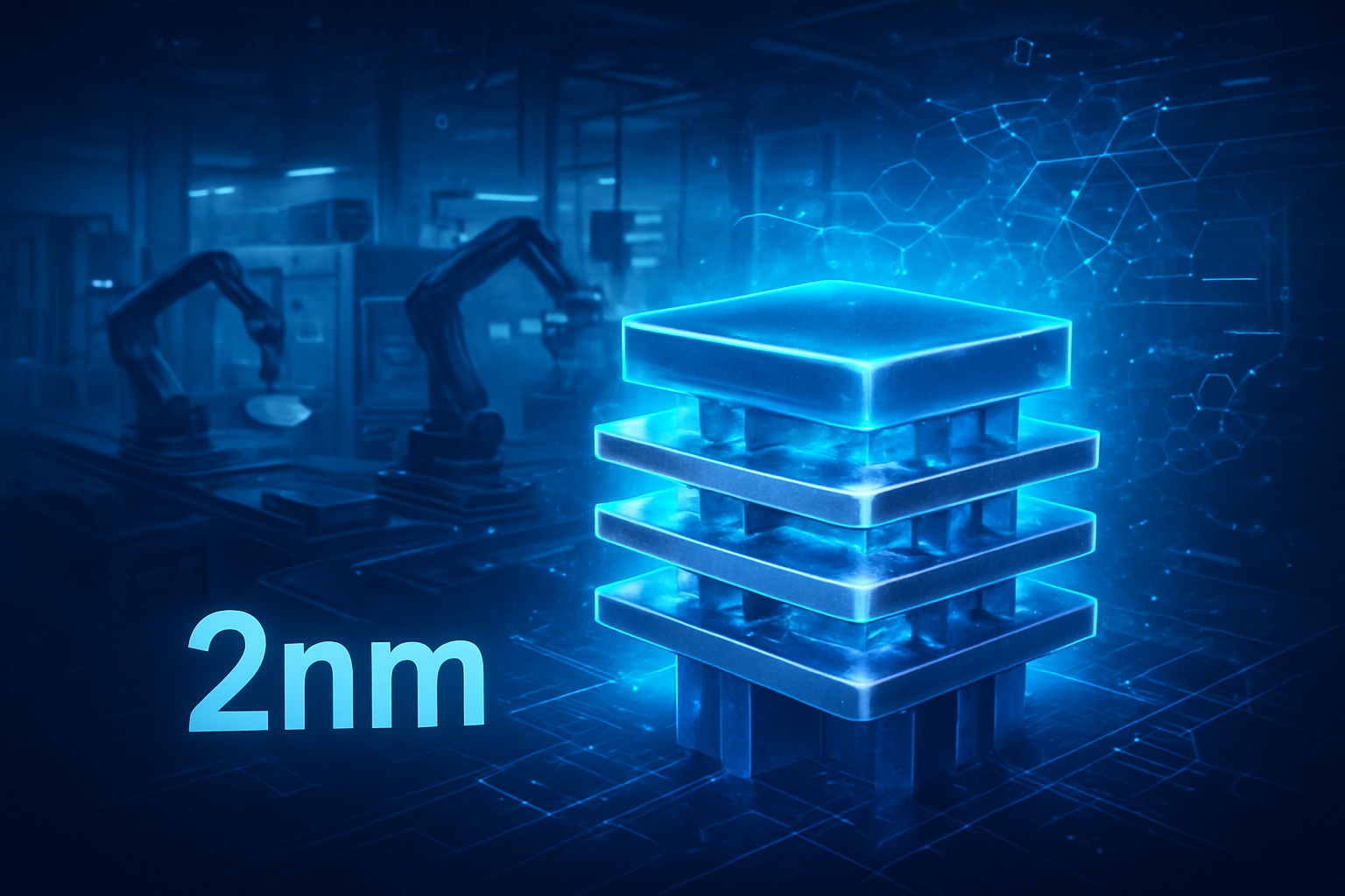
    The Intel 18A node represents the most significant architectural shift in transistor design since the introduction of FinFET over ten years ago. At the heart of this advancement is RibbonFET, Intel’s implementation of Gate-All-Around (GAA) technology. By wrapping the gate entirely around the transistor channel, Intel has achieved superior electrostatic control, drastically reducing current leakage and enabling a reported 15% increase in performance-per-watt over the previous Intel 3 node. This allows AI workloads to run faster while consuming less energy, a critical requirement for the heat-constrained environments of modern data centers.

    Complementing RibbonFET is PowerVia, a first-to-market innovation in backside power delivery. Traditionally, power and signal lines are crowded together on the top of a wafer, leading to interference and "voltage droop." By moving the power delivery to the back of the silicon, Intel has decoupled these functions, reducing voltage droop by as much as 30%. Industry analysts from TechInsights have noted that this "architectural lead" gives Intel a temporary advantage in efficiency over TSMC (NYSE: TSM), which is not expected to implement a similar solution at scale until later in 2026.

    Initial reactions from the semiconductor research community have been overwhelmingly positive, though tempered by the reality of the task ahead. While Intel 18A’s transistor density of roughly 238 MTr/mm² is slightly lower than the projected density of TSMC’s upcoming N2 node, experts agree that the layout efficiencies provided by PowerVia more than compensate for the raw density gap. The consensus among hardware engineers is that Intel has moved from "playing catch-up" to "setting the pace" for power-efficient high-performance computing.

    A New Power Dynamic: Disrupting the Foundry Landscape

    The success of 18A has massive implications for the global foundry market, where Intel is positioning itself as a Western-based alternative to TSMC and Samsung Electronics (KRX: 005930). Intel Foundry has already secured high-profile "design wins" that validate the 18A node's capabilities. Microsoft (NASDAQ: MSFT) has confirmed it will use 18A for its Maia 3 AI accelerators, and Amazon (NASDAQ: AMZN) is leveraging the node for its AWS-specific silicon. Even the U.S. Department of Defense has signed on, utilizing the 18A process to ensure a secure, domestic supply chain for sensitive defense electronics.

    For the "AI PC" market, the arrival of Panther Lake is a strategic masterstroke. Launched officially at CES 2026, these chips feature a next-generation Neural Processing Unit (NPU) and Xe3 graphics, delivering a 77% boost in gaming performance and significantly enhanced local AI processing. This puts Intel in a dominant position to capture a predicted 55% share of the AI PC market by the end of 2026, challenging Apple (NASDAQ: AAPL) and its M-series silicon on both performance and battery life.

    In the data center, Clearwater Forest (Xeon 6+) is designed to fend off the rise of ARM-based competitors. By utilizing "Darkmont" E-cores and the efficiency of the 18A node, Intel is providing hyperscalers with a path to scale their AI and cloud infrastructure without a linear increase in power consumption. This shift poses a direct threat to the market positioning of custom silicon efforts from cloud providers, as Intel can now offer comparable or superior performance-per-watt through its standard server offerings or its foundry services.

    Restoring Moore’s Law in the Age of Artificial Intelligence

    The wider significance of Intel 18A extends beyond mere performance metrics; it represents a fundamental pivot in the broader AI landscape. As AI models grow in complexity, the demand for "compute density" has become the primary bottleneck for innovation. Intel’s ability to deliver a high-volume, power-efficient node like 18A helps alleviate this pressure, potentially lowering the cost of training and deploying large-scale AI models.

    Furthermore, this development marks a geopolitical victory for U.S.-based manufacturing. By successfully executing the 5N4Y roadmap, Intel has proved that leading-edge semiconductor fabrication can still thrive on American soil. This achievement aligns with the goals of the CHIPS and Science Act, providing a domestic safeguard against the supply chain vulnerabilities that have plagued the industry in recent years. Comparisons are already being made to the 2011 transition to 22nm FinFET, with many historians viewing the 18A HVM launch as the moment Intel definitively broke its "stagnation era."

    However, potential concerns remain regarding the long-term profitability of Intel’s foundry business. While the technical milestones have been met, the capital expenditure required to maintain this pace is astronomical. Critics point out that while Intel has closed the process gap, it must now prove it can maintain the high yields and service levels required to steal significant market share from TSMC, which remains the gold standard for foundry operations.

    The Road to 14A and Beyond: What Lies Ahead

    With the 5N4Y roadmap now in the rearview mirror, Intel is looking toward the end of the decade. The company has already detailed its post-18A plans, which focus on Intel 14A (1.4nm) and eventually Intel 10A. These future nodes will likely lean even more heavily into High-NA EUV (Extreme Ultraviolet) lithography, a technology Intel has pioneered ahead of its peers. The near-term focus will be on the 18A-P update, a refined version of the current node designed to wring out even more efficiency for the 2027 product cycle.

    On the horizon, we expect to see 18A applied to an even wider array of use cases, from autonomous vehicle systems to edge-computing AI for industrial robotics. Experts predict that the next two years will be a period of "optimization and expansion," where Intel works to bring more external customers onto its 18A and 14A lines. The challenge will be scaling this technology across multiple fabs globally while keeping costs competitive for smaller startups that are currently priced out of leading-edge silicon.

    A Milestone in Semiconductor History

    The official HVM launch of Intel 18A is more than just a product release; it is the culmination of one of the most aggressive turnaround efforts in industrial history. By delivering five process nodes in four years, Intel has silenced skeptics and re-established its technical credibility. The significance of this achievement in the context of the AI revolution cannot be overstated—AI requires hardware that is not only fast but sustainably efficient, and 18A is the first node designed from the ground up to meet that need.

    In the coming weeks and months, the industry will be watching the initial retail rollout of Panther Lake laptops and the performance benchmarks of Clearwater Forest in live data center environments. If the reported 65-75% yields continue to improve, Intel will have not only met its roadmap but set a new standard for the industry. For now, the "5 Nodes in 4 Years" saga ends on a triumphant note, leaving the semiconductor giant well-positioned to lead the next era of AI-driven computing.


    This content is intended for informational purposes only and represents analysis of current AI developments.

    TokenRing AI delivers enterprise-grade solutions for multi-agent AI workflow orchestration, AI-powered development tools, and seamless remote collaboration platforms.
    For more information, visit https://www.tokenring.ai/.

  • Intel’s 18A Node Secures Interest from Apple and NVIDIA, Reshaping Global Chip Foundries by 2028

    Intel’s 18A Node Secures Interest from Apple and NVIDIA, Reshaping Global Chip Foundries by 2028

    In a historic shift for the semiconductor industry, Intel Corporation (NASDAQ: INTC) has successfully positioned its 18A process node as a viable domestic alternative for the world’s most demanding chip designers. As of February 2, 2026, reports indicate that both Apple Inc. (NASDAQ: AAPL) and NVIDIA (NASDAQ: NVDA) have entered advanced discussions to utilize Intel’s U.S.-based foundries for high-volume production starting in 2028. This development marks a significant milestone in Intel’s "five nodes in four years" strategy, moving the company from a struggling manufacturer to a formidable competitor against the long-standing dominance of TSMC (NYSE: TSM).

    The immediate significance of this announcement cannot be overstated. For years, the global technology supply chain has been precariously reliant on Taiwanese manufacturing. The news that Apple is exploring Intel 18A for its entry-level M-series chips and that NVIDIA is eyeing the node for its next-generation "Feynman" GPU components suggests a major rebalancing of the silicon landscape. By securing interest from these industry titans, Intel Foundry has validated its technical roadmap and provided a strategic "pressure valve" for an industry currently constrained by limited advanced-node capacity.

    The Technical Edge: RibbonFET and PowerVia Come to Life

    Intel’s 18A (1.8nm) process node reached High-Volume Manufacturing (HVM) status in late January 2026, with Fab 52 in Arizona now operational and producing roughly 40,000 wafers per month. The technical superiority of 18A lies in two foundational innovations: RibbonFET and PowerVia. RibbonFET is Intel’s implementation of Gate-All-Around (GAA) transistor architecture, which allows for finer control over the channel current, reducing leakage and boosting performance-per-watt. PowerVia, the industry’s first backside power delivery solution, moves power routing to the back of the wafer. This reduces voltage droop and frees up the top layers for signal routing, a leap that analysts suggest gives Intel a six-to-twelve-month lead over TSMC’s implementation of similar technology.

    Initial yields for 18A are currently reported in the 55–65% range, a "predictable ramp" that is expected to hit world-class efficiency of over 75% by early 2027. Unlike previous Intel nodes that suffered from delays, the 18A transition has been buoyed by the successful deployment of internal products like the "Panther Lake" Core Ultra Series 3 and "Clearwater Forest" Xeon processors. Industry experts note that 18A's performance-to-density ratio is now competitive with TSMC’s N2 node, offering a compelling technical alternative for companies that have traditionally been "locked in" to the Taiwanese ecosystem.

    A Strategic Pivot for Apple and NVIDIA

    The interest from Apple and NVIDIA represents a calculated move to diversify supply chains and mitigate risk. Apple is reportedly eyeing the Intel 18A-P (performance-enhanced) variant for its 2028 lineup of entry-level M-series chips, intended for the MacBook Air and iPad. While the flagship "Pro" and "Max" chips will likely remain with TSMC for the time being, utilizing Intel for high-volume, cost-sensitive silicon allows Apple to secure more favorable pricing and guaranteed capacity. Similarly, Apple is exploring Intel’s 14A (1.4nm) node for non-Pro iPhone A-series chips, signaling a long-term commitment to Intel’s foundry services.

    NVIDIA’s engagement is even more transformative. Facing an insatiable demand for AI hardware, NVIDIA has reportedly taken a 5% stake in Intel Foundry, a $5 billion investment aimed at securing domestic capacity for its 2028 "Feynman" GPU architecture. While the primary compute dies may stay with TSMC, NVIDIA plans to outsource the I/O dies and a significant portion of its advanced packaging to Intel. Specifically, Intel’s EMIB (Embedded Multi-die Interconnect Bridge) technology is being positioned as a crucial alternative to TSMC’s CoWoS packaging, which has been a major bottleneck in the AI supply chain throughout 2024 and 2025.

    Geopolitics and the Reshoring Revolution

    The shift toward Intel is driven as much by geopolitics as by nanometers. As of 2026, the concentration of advanced semiconductor manufacturing in Taiwan is viewed as a "single point of failure" by both corporate boards and the U.S. government. The CHIPS Act and subsequent domestic policy initiatives have provided the financial scaffolding for Intel to build its "Silicon Heartland" in Arizona and Ohio. For Apple and NVIDIA, moving a portion of their production to U.S. soil is an insurance policy against regional instability and potential trade tariffs that could penalize offshore manufacturing.

    This movement also aligns with the broader AI boom, which has created a structural shortage of advanced fabrication capacity. As Microsoft (NASDAQ: MSFT) and Amazon (NASDAQ: AMZN) continue to scale their custom AI silicon on Intel’s 18A node, the foundry has proven it can handle the scale required by "hyperscalers." The entry of Apple and NVIDIA into the Intel ecosystem effectively ends the TSMC monopoly on leading-edge logic, creating a healthier, multi-polar foundry market that could accelerate the pace of innovation across the entire tech sector.

    The Roadmap to 14A and Beyond

    Looking forward, the partnership between Intel and these tech giants is expected to deepen as the industry moves toward the 14A (1.4nm) era. The primary challenge remains the "porting" of complex chip designs. Intel is currently rolling out Process Design Kits (PDKs) that are more compatible with industry-standard EDA tools, making it easier for Apple and NVIDIA engineers to transition their designs from TSMC’s libraries to Intel’s. Analysts predict that if the 18A production ramp continues without hitches, Intel could capture up to 20% of the external advanced foundry market by 2030.

    Beyond 2028, we expect to see Intel’s Arizona and Ohio fabs becoming the primary hubs for "secure silicon," with the U.S. Department of Defense and major Western enterprises prioritizing domestic production. The upcoming 14A node, scheduled for 2027-2028, will likely be the stage for the next great performance battle. If Intel can maintain its execution momentum, it may not just be a secondary source for Apple and NVIDIA, but a preferred partner for their most advanced, AI-integrated consumer and data center products.

    A New Era for Silicon

    The convergence of Intel’s technical resurgence and the strategic needs of Apple and NVIDIA marks the beginning of a new era in computing. For Intel, securing these customers is the ultimate validation of CEO Pat Gelsinger’s turnaround plan. It transforms the company from a legacy chipmaker into the cornerstone of a new, geographically diverse semiconductor supply chain. For the tech industry, it provides much-needed competition in a sector that has been dangerously centralized for over a decade.

    In the coming months, all eyes will be on the yield reports from Fab 52 and the finalization of the 2028 production contracts. While TSMC remains the undisputed leader in volume and ecosystem maturity, Intel’s 18A node has officially broken the glass ceiling. The "Silicon Renaissance" is no longer a marketing slogan—it is a $100 billion reality that will define the performance of the iPhones, MacBooks, and AI GPUs of the late 2020s.


    This content is intended for informational purposes only and represents analysis of current AI developments.

    TokenRing AI delivers enterprise-grade solutions for multi-agent AI workflow orchestration, AI-powered development tools, and seamless remote collaboration platforms.
    For more information, visit https://www.tokenring.ai/.

  • Samsung Taylor Fab Commences Risk Production for 2nm Chips

    Samsung Taylor Fab Commences Risk Production for 2nm Chips

    In a move that signals a seismic shift in the global semiconductor landscape, Samsung Electronics (KRX: 005930) has officially commenced risk production for its 2nm (SF2) process node at its $44 billion facility in Taylor, Texas. This milestone marks the first time that cutting-edge 2nm-class silicon has been manufactured on U.S. soil, representing a critical victory for Samsung in its bid to challenge the dominance of Taiwan Semiconductor Manufacturing Company (TPE: 2330).

    The Taylor facility, which has transitioned from its original 4nm mandate to a "2nm-first" strategy, is now operating its first batch of advanced lithography systems. This development is not merely a technical achievement; it is a foundational pillar of the U.S. strategy to secure domestic leading-edge chip production. Supported by $6.4 billion in subsidies from the CHIPS and Science Act, Samsung’s Texas operations are now the epicenter of a "Turnkey" manufacturing ecosystem designed to provide the world’s most advanced AI hardware under one roof.

    Technical Prowess: Third-Generation GAA and CNT Pellicles

    The 2nm process, designated as SF2 by Samsung Foundry, utilizes the third generation of the company’s proprietary Gate-All-Around (GAA) architecture, branded as Multi-Bridge Channel FET (MBCFET). While competitors like TSMC are just beginning their transition to GAA at the 2nm level, Samsung is leveraging nearly four years of telemetry data from its early 3nm GAA production. The SF2 node delivers a 12% increase in performance and a 25% reduction in power consumption compared to the previous 3nm generation. This efficiency is critical for the next wave of hyperscale AI accelerators and mobile processors that are pushing the limits of thermal management.

    A key differentiator in the Taylor fab’s 2nm line is the large-scale implementation of advanced Extreme Ultraviolet (EUV) pellicles. Samsung has adopted Carbon Nanotube (CNT) pellicle technology, which boasts a light transmittance rate exceeding 97%. This is a significant upgrade over traditional silicon-based pellicles, which often suffer from lower transparency and thermal degradation under the high-power EUV beams required for 2nm patterning. By reducing "stochastic" defects and increasing wafer throughput, these CNT pellicles are expected to help Samsung achieve a target yield of 60-70%—a figure that would make it highly competitive with TSMC’s N2 node.

    Furthermore, Samsung is preparing its SF2P (Performance) variant for high-end data center applications, which features specialized channel strain engineering to reduce parasitic capacitance. Initial reactions from the industry have been cautiously optimistic; while Samsung struggled with early 3nm yields, the stabilization of its 2nm process in Taylor suggests that the company has finally overcome the learning curve associated with GAA structures.

    Market Dynamics: Courting AMD, Qualcomm, and Tesla

    Samsung’s strategic pivot to the United States is already paying dividends in terms of customer acquisition. Advanced Micro Devices (NASDAQ: AMD) and Qualcomm (NASDAQ: QCOM) are reportedly in deep negotiations to secure 2nm capacity at the Taylor fab. For Qualcomm, the attraction lies in Samsung’s ability to offer a "dual-sourcing" alternative to TSMC, where Apple has reportedly reserved the lion's share of initial 2nm capacity. Industry insiders suggest that Samsung’s 2nm wafers could be priced as much as 33% lower than TSMC’s, providing a vital margin cushion for chip designers facing rising manufacturing costs.

    The Taylor fab has also secured a cornerstone client in Tesla (NASDAQ: TSLA). The electric vehicle giant is expected to use the facility for its next-generation AI6 autonomous driving chips. By fabbing these chips in Texas, Tesla gains a localized supply chain that minimizes geopolitical risk and logistical overhead. This "Made in USA" advantage is becoming a primary selling point as tech giants look to diversify their manufacturing footprint away from East Asia.

    The competitive landscape is further complicated by Intel (NASDAQ: INTC), which has recently ramped up its 18A node. While Intel currently holds a lead in backside power delivery technology, Samsung’s "Turnkey Strategy"—which integrates 2nm logic, HBM4 memory, and advanced 3D packaging (SAINT)—offers a comprehensive solution that Intel and TSMC struggle to match individually. This holistic approach is particularly attractive to AI startups and hyperscalers that require high-bandwidth memory to be stacked directly onto 2nm logic dies.

    Geopolitics and the AI Hardware Explosion

    The commencement of 2nm risk production in Taylor is a landmark moment in the broader AI landscape. As the demand for NVIDIA (NASDAQ: NVDA) GPUs and custom AI ASICs continues to outpace supply, the addition of a major 2nm hub in the United States provides a necessary safety valve for the industry. It aligns perfectly with the current trend toward sovereign AI, where nations and corporations seek to control their hardware destiny.

    This development also underscores the success of the CHIPS Act in incentivizing leading-edge manufacturing within the U.S. The Taylor campus, now a $44 billion investment, represents one of the largest foreign direct investments in U.S. history. By fostering a "K-Semiconductor Cluster" in Central Texas—including specialized suppliers for EUV pellicles and materials—Samsung is building an ecosystem that will likely influence semiconductor trends for the next decade.

    However, concerns remain regarding the speed of the yield ramp. While 60% yield is a strong start for 2nm, the industry standard for high-volume profitability typically requires upwards of 70-80%. Comparisons to previous milestones, such as the move from 7nm to 5nm, show that the transition to 2nm is orders of magnitude more complex due to the extreme precision required in lithography and the fragility of nanosheet structures.

    The Horizon: From Risk Production to 1.4nm

    Looking ahead, Samsung plans to transition from risk production to full-scale mass production at the Taylor fab by the second half of 2026. This timeline puts them in a neck-and-neck race with TSMC’s Arizona facility. In the near term, we can expect to see the first 2nm-powered consumer devices, likely headlined by Samsung's own Galaxy S27 series and potentially a refreshed line of AI-capable laptops from various OEMs.

    Beyond 2nm, Samsung has already laid out a roadmap for its 1.4nm (SF1.4) node, which is slated for development by late 2027. The Taylor fab is designed to be future-proof, with the infrastructure already in place to support the move to "High-NA" EUV systems from ASML (NASDAQ: ASML) as they become commercially viable. The primary challenge moving forward will be the integration of Backside Power Delivery (BSPDN) in the SF2Z variant, which experts predict will be the next major battleground in semiconductor architecture.

    A Final Assessment of the Taylor Milestone

    The commencement of 2nm risk production at Samsung’s Taylor fab is a definitive "coming of age" moment for the U.S. semiconductor industry and a bold statement of intent from Samsung. By combining its 3rd-generation GAA technology with a multi-billion dollar commitment to American manufacturing, Samsung is not just building a factory; it is attempting to rewrite the rules of the foundry market.

    The significance of this development in AI history cannot be overstated. As AI models become more complex, the hardware that powers them must become more efficient and accessible. The Taylor facility provides the capacity and the cutting-edge tech to meet that demand. In the coming weeks and months, the industry will be watching Samsung’s yield reports and customer announcements closely. If the company can maintain its current momentum, the "Silicon Hills" of Texas may soon become the most important real estate in the global AI economy.


    This content is intended for informational purposes only and represents analysis of current AI developments.

    TokenRing AI delivers enterprise-grade solutions for multi-agent AI workflow orchestration, AI-powered development tools, and seamless remote collaboration platforms.
    For more information, visit https://www.tokenring.ai/.

  • Intel Reclaims the Silicon Throne: 18A Enters High-Volume Production, Completing the ‘5 Nodes in 4 Years’ Odyssey

    Intel Reclaims the Silicon Throne: 18A Enters High-Volume Production, Completing the ‘5 Nodes in 4 Years’ Odyssey

    Intel (NASDAQ: INTC) has officially declared victory in its most ambitious engineering campaign to date, announcing today, January 30, 2026, that its Intel 18A process node has entered high-volume manufacturing (HVM). This milestone marks the formal completion of the company’s "5 Nodes in 4 Years" (5N4Y) roadmap, a high-stakes strategy initiated by CEO Pat Gelsinger in 2021 to restore the company to the vanguard of semiconductor manufacturing. With the commencement of HVM for the "Panther Lake" mobile processors and "Clearwater Forest" server chips, Intel has not only met its self-imposed deadline but has also effectively leapfrogged its rivals in several key architectural transitions.

    The successful ramp of 18A represents a seismic shift for the global technology sector. By reaching this stage, Intel has validated its move toward a "foundry-first" business model, aimed at challenging the dominance of Taiwan Semiconductor Manufacturing Company (NYSE: TSM). The transition is already bearing fruit, with the company securing significant design wins from hyperscale giants and defense agencies. As the industry grapples with the escalating demands of generative AI, the 18A node provides the dense, power-efficient foundation required for the next generation of neural processing units (NPUs) and massive multi-core data center architectures.

    The Technical Triumph of 18A: RibbonFET and PowerVia

    The Intel 18A node is more than just a reduction in feature size; it introduces two fundamental architectural changes that the industry has not seen in over a decade. The first is RibbonFET, Intel’s implementation of Gate-All-Around (GAA) transistor technology. Unlike the FinFET transistors used since 2011, RibbonFET wraps the gate entirely around the transistor channel on all four sides. This allows for superior electrical control, significantly reducing current leakage while enabling higher drive currents. In practical terms, 18A offers approximately a 15% improvement in performance-per-watt over the preceding Intel 3 node, allowing chips to run faster without exceeding thermal limits.

    Equally revolutionary is PowerVia, Intel's proprietary backside power delivery system. Historically, power and signal wires were layered together on top of the silicon, creating a "spaghetti" of interconnects that led to electrical interference and power loss. PowerVia moves the power delivery circuitry to the reverse side of the wafer, separating it entirely from the signal lines. This architectural shift reduces "voltage droop" (IR drop) by up to 30%, which translates directly into a 6% boost in clock frequency or a significant reduction in power consumption. By clearing the congestion on the top of the die, Intel has also managed to increase transistor density by nearly 10% compared to traditional routing methods.

    The dual-pronged launch of Panther Lake and Clearwater Forest showcases these technologies in action. Panther Lake, the new flagship for the Core Ultra Series 3, features the "Cougar Cove" performance cores and the "Darkmont" efficiency cores, alongside a third-generation Xe3 integrated GPU. Notably, it includes an NPU 5 capable of delivering over 50 TOPS (Trillions of Operations Per Second), setting a new bar for on-device AI in thin-and-light laptops. Meanwhile, Clearwater Forest targets the cloud, featuring up to 288 E-cores per socket. It utilizes 18A compute dies stacked onto Intel 3 base tiles using Foveros Direct 3D packaging, a testament to Intel's growing prowess in advanced heterogeneous integration.

    A New Competitive Reality for Foundry Giants

    The success of 18A has fundamentally altered the competitive landscape between Intel, TSMC, and Samsung (KRX: 005930). While TSMC still maintains a slight edge in raw transistor density, Intel has claimed a significant "first-mover" advantage in backside power delivery. TSMC’s equivalent technology, known as Super Power Rail, is not expected to reach high-volume production until its A16 node in late 2026. This window of technical leadership has allowed Intel to secure "whale" customers that previously relied solely on Asian foundries.

    The immediate beneficiaries are tech giants looking to reduce their dependence on a single source of supply. Microsoft (NASDAQ: MSFT) has confirmed that its next-generation Maia AI accelerators will be built on 18A, while Amazon (NASDAQ: AMZN) is utilizing the node for its custom AI fabric chips. Other confirmed partners include Ericsson for 5G infrastructure and Faraday Technology for a 64-core Arm-based SoC. Even companies like NVIDIA (NASDAQ: NVDA) and Broadcom (NASDAQ: AVGO), which have traditionally been loyal to TSMC, are reportedly in active testing phases with 18A. Though Broadcom expressed initial concerns regarding yields in 2025, Intel’s report of 55–75% yield rates in early 2026 suggests the process has matured enough to support high-volume commercial contracts.

    For the broader market, Intel’s resurgence provides a much-needed strategic alternative. The concentration of leading-edge logic manufacturing in Taiwan has long been a point of geopolitical concern. With Intel's 18A reaching maturity in its Oregon and Arizona facilities, the "silicon shield" is effectively expanding to North America. This geographic diversification is a strategic advantage for firms like Apple (NASDAQ: AAPL), which is rumored to be qualifying an enhanced 18A-P variant for its 2027 product lineup.

    Geopolitical and Historical Significance in the AI Era

    The completion of the "5 Nodes in 4 Years" plan is likely to be remembered as one of the most significant turnarounds in industrial history. It marks the end of an era where Intel was often viewed as a "stumbling giant" that had lost its way during the transition to Extreme Ultraviolet (EUV) lithography. By successfully navigating the technical hurdles of 18A, Intel has validated that Moore's Law is not dead but has simply moved into a more complex, three-dimensional phase. This milestone is comparable to the 2011 introduction of the FinFET, which sustained the industry for the last 15 years.

    Furthermore, the 18A launch is intrinsically tied to the "AI Gold Rush." As generative AI shifts from massive data centers to local "Edge AI" devices, the performance-per-watt gains of RibbonFET and PowerVia become critical. Without these architectural improvements, the power requirements for running large language models (LLMs) on mobile devices would be prohibitive. Intel’s ability to mass-produce these chips domestically also aligns with the goals of the U.S. CHIPS and Science Act, providing a secure, leading-edge manufacturing base for the U.S. Department of Defense (DoD), which is already a confirmed 18A customer through the RAMP-C program.

    However, challenges remain. The massive capital expenditure required to build these "Mega-Fabs" has put significant pressure on Intel’s margins. While the technology is a success, the financial sustainability of the foundry business depends on maintaining high utilization rates from external customers. The industry is watching closely to see if Intel can sustain this momentum without the "heroic" engineering efforts that defined the 5N4Y sprint.

    The Road Ahead: 14A and High-NA EUV

    Looking toward the future, Intel is already preparing its next major leap: the Intel 14A node. While 18A is the current state-of-the-art, 14A is being designed as the "war node" that Intel hopes will secure undisputed leadership through the end of the decade. This upcoming process will be the first to fully integrate High-NA EUV (High Numerical Aperture) lithography, utilizing the advanced ASML (NASDAQ: ASML) systems that Intel was the first in the industry to acquire.

    Near-term developments include the release of the Process Design Kit (PDK) 0.5 for 14A in early 2026, allowing designers to begin mapping out 1.4nm-class chips. We can also expect to see the introduction of PowerDirect, an evolutionary step beyond PowerVia that further optimizes power delivery. Intel has signaled a more disciplined "customer-first" approach for 14A, stating it will only expand capacity once firm commitments are signed, a move meant to appease investors worried about over-expansion.

    A Defining Moment for the Semiconductor Industry

    The successful launch of 18A and the completion of the 5N4Y roadmap represent a pivotal "mission accomplished" moment for Intel. The company has moved from a position of technical obsolescence to a position where it is defining the industry’s architectural standards for the next decade. The immediate rollout of Panther Lake and Clearwater Forest provides a tangible proof of concept that the technology is ready for prime time.

    As we look toward the rest of 2026, the key metrics to watch will be the "foundry ramp"—specifically, whether more high-volume customers like MediaTek or Apple formally commit to 18A production. The technical victory is won; the commercial victory is the next frontier. Intel has successfully rebuilt its engine while flying the plane, and for the first time in years, the company is no longer chasing the leaders of the semiconductor world—it is standing right beside them.


    This content is intended for informational purposes only and represents analysis of current AI developments.

    TokenRing AI delivers enterprise-grade solutions for multi-agent AI workflow orchestration, AI-powered development tools, and seamless remote collaboration platforms.
    For more information, visit https://www.tokenring.ai/.

  • Samsung Hits 70% Yield on 2nm GAA (SF2P): A Turning Point for the AI Chip Supply Chain

    Samsung Hits 70% Yield on 2nm GAA (SF2P): A Turning Point for the AI Chip Supply Chain

    As of January 30, 2026, the global semiconductor landscape is undergoing a tectonic shift. Samsung Electronics (KRX: 005930) has officially reached a critical performance and yield milestone for its 2nm (SF2P) production process, signaling a major challenge to the long-standing dominance of Taiwan Semiconductor Manufacturing Company (NYSE: TSM). Following its Q4 2025 earnings report, Samsung confirmed that its performance-optimized 2nm node, known as SF2P, has successfully hit the 70% yield threshold required for stable mass production—a feat that many industry skeptics thought would take years to master.

    This development is more than just a technical victory; it is a strategic lifeline for the world’s largest chip designers. With TSMC’s 2nm capacity currently overwhelmed by exclusive orders from high-priority clients, the emergence of a viable, high-yield alternative from Samsung provides a release valve for a supply chain that has been dangerously bottlenecked. By mastering the intricate Gate-All-Around (GAA) architecture ahead of its rivals, Samsung is positioning itself as the primary destination for the next generation of high-performance AI and mobile processors.

    Engineering the Future: The Maturity of 3rd-Gen GAA

    The SF2P node represents the second generation of Samsung’s 2nm platform, specifically optimized for high-performance computing (HPC) and premium mobile devices. Unlike traditional FinFET transistors, which hit physical scaling limits years ago, Samsung’s 2nm utilizes its proprietary Multi-Bridge Channel FET (MBCFET) architecture—a 3rd-generation evolution of GAA technology. This approach allows for a "nanosheet" design where the width of the channel can be adjusted to optimize for either extreme power efficiency or maximum performance. Compared to the first-generation SF2 node, the 2026-era SF2P delivers a 12% boost in clock speeds, a 25% improvement in power efficiency, and an 8% reduction in total die area.

    Technical experts note that Samsung’s early gamble on GAA—which it first introduced at the 3nm node while TSMC stuck with FinFET—is finally paying dividends. While competitors are only now navigating the "learning curve" of nanosheet production, Samsung has accumulated four years of telemetry data on GAA manufacturing. This experience has allowed the foundry to refine its extreme ultraviolet (EUV) lithography processes and address the "stochastic" defects that typically plague sub-3nm nodes. The result is a more uniform transistor structure that significantly reduces leakage current, a critical requirement for the power-hungry AI workloads of 2026.

    A Strategic Pivot: Qualcomm and AMD Secure Capacity

    The immediate beneficiaries of Samsung’s yield breakthrough are Qualcomm (NASDAQ: QCOM) and AMD (NASDAQ: AMD). As of late January 2026, both companies are reportedly in final negotiations to shift significant portions of their 2nm roadmap to Samsung Foundry. The move is driven by a stark reality: TSMC’s 2nm (N2) capacity is nearly 50% reserved by a single customer, leaving other tech giants fighting for leftovers and paying a "wafer premium" that has risen 50% over previous generations. Qualcomm is expected to utilize SF2P for its next-generation Snapdragon series, while AMD is eyeing the node for its "Venice" EPYC server CPUs to ensure supply stability in the face of skyrocketing enterprise demand.

    This shift represents a significant competitive disruption. For years, TSMC’s "foundry-only" model gave it a reputation for neutrality and reliability that Samsung, a conglomerate that also makes its own consumer products, struggled to match. However, the sheer scale of the AI boom has forced a "dual-sourcing" strategy among major chip designers. By offering competitive yields and more favorable pricing than TSMC, Samsung is transforming the foundry market from a monopoly into a true duopoly. Furthermore, Samsung’s massive $16.5 billion contract with Tesla (NASDAQ: TSLA) for its AI6 autonomous driving chips has served as a powerful "seal of approval," encouraging other automotive and data center players to reconsider their reliance on a single supplier.

    The "One-Stop" AI Solution and the Taylor, Texas Factor

    Samsung’s 2nm success is part of a broader "total solution" strategy that integrates logic, memory, and packaging. In January 2026, Samsung began large-scale shipments of its 12-layer HBM4 (High Bandwidth Memory), a key component for AI accelerators used by NVIDIA (NASDAQ: NVDA) and others. By offering 2nm logic manufacturing alongside HBM4 and advanced X-Cube 3D packaging, Samsung provides a vertically integrated stack that reduces latency and power consumption. This "one-stop shop" capability is something neither TSMC nor Intel (NASDAQ: INTC) can currently match with the same level of internal synchronization, making Samsung an attractive partner for startups building custom "Agentic AI" silicon.

    The geopolitical dimension of this ramp-up cannot be ignored. Samsung’s Taylor, Texas facility is now 93% complete and is transitioning to a "2nm-first" factory. With trial runs of ASML EUV lithography tools scheduled for March 2026, the Taylor fab is set to become a cornerstone of the "Made in USA" advanced chip initiative. This domestic capacity is a major selling point for U.S.-based companies like AMD and Google, who are under increasing pressure to diversify their manufacturing away from the geopolitical sensitivities of the Taiwan Strait. Samsung’s ability to hit 70% yield in its Korean facilities provides the blueprint for a rapid and successful ramp in the United States.

    Looking Ahead: The Road to 1.4nm and Backside Power

    While the industry focuses on the SF2P ramp, Samsung’s R&D teams are already moving toward the next frontier. Near-term developments include the introduction of SF2Z in 2027, which will incorporate Backside Power Delivery Network (BSPDN) technology. This innovation moves the power circuitry to the back of the wafer, freeing up the top side for more transistors and further reducing voltage drops. Beyond 2nm, the roadmap points toward the 1.4nm (SF1.4) node, where Samsung expects to apply lessons from its GAA maturity to achieve even more aggressive density gains.

    The challenge remains in maintaining these yields as the volume scales to hundreds of thousands of wafers per month. Experts predict that the next 12 months will be a "volume war" as Samsung attempts to match the total output capacity of TSMC’s sprawling "GigaFabs." Additionally, as AI models move from data centers to "on-device" edge environments, the demand for SF2P-class chips will expand into a wider variety of form factors, including wearable AR glasses and advanced robotics. The primary hurdle will be the continued availability of high-NA EUV tools and the specialized gases required for sub-2nm etching.

    A New Era for the Semiconductor Industry

    Samsung’s achievement of 70% yield on the SF2P node marks a historic comeback for the South Korean giant. After years of trailing TSMC in the transition from 7nm to 5nm and 4nm, Samsung has utilized the radical architecture shift of Gate-All-Around to leapfrog its competition in terms of manufacturing maturity. This development effectively breaks the "TSMC bottleneck," providing the global AI industry with the diversified supply chain it desperately needs to sustain its current pace of innovation.

    In the coming weeks, the industry will be watching for the official "tape-out" announcements from Qualcomm and AMD, which will confirm the first commercial products to use this new technology. The successful integration of SF2P into the global supply chain will not only redefine Samsung’s financial trajectory but will also serve as a catalyst for more affordable and efficient AI hardware worldwide. As we move deeper into 2026, the foundry race has officially been reset, and for the first time in a decade, the lead is up for grabs.


    This content is intended for informational purposes only and represents analysis of current AI and semiconductor developments.

    TokenRing AI delivers enterprise-grade solutions for multi-agent AI workflow orchestration, AI-powered development tools, and seamless remote collaboration platforms.
    For more information, visit https://www.tokenring.ai/.

  • Intel Reclaims the Silicon Throne: 18A Node Hits High-Volume Production, Ending a Five-Year Marathon

    Intel Reclaims the Silicon Throne: 18A Node Hits High-Volume Production, Ending a Five-Year Marathon

    In a historic turning point for the American semiconductor industry, Intel (NASDAQ: INTC) officially announced this month that its 18A process node has reached high-volume manufacturing (HVM) status. This milestone marks the formal completion of the company’s "five nodes in four years" (5N4Y) roadmap, a high-stakes engineering sprint initiated in 2021 that many industry skeptics once deemed impossible. As of January 30, 2026, Intel has not only met its self-imposed deadline but has also successfully transitioned its first wave of 18A-based products, including the "Panther Lake" consumer chips and "Clearwater Forest" Xeon processors, into mass production.

    The achievement is being hailed as the most significant shift in the global foundry landscape in over a decade. By reaching HVM ahead of its primary competitors' equivalent nodes, Intel has effectively closed the "process gap" that allowed rivals to dominate the high-performance computing market for years. For the first time since the mid-2010s, the Santa Clara giant can plausibly claim the lead in transistor architecture and power delivery, positioning itself as the premier domestic alternative for the world’s most demanding AI and data center workloads.

    The Engineering Trifecta: RibbonFET, PowerVia, and 18A

    The transition to Intel 18A is more than a simple shrink in transistor size; it represents a fundamental overhaul of how semiconductors are built. Central to this leap are two foundational technologies: RibbonFET and PowerVia. RibbonFET is Intel’s implementation of a Gate-All-Around (GAA) transistor architecture, which replaces the long-standing FinFET design. By surrounding the transistor channel on all four sides, RibbonFET provides superior control over electrical leakage and higher drive currents, resulting in a 15% improvement in performance-per-watt over the previous Intel 3 node. This enables chips to run faster while consuming less power—a critical requirement for the energy-hungry AI era.

    Equally transformative is PowerVia, Intel’s proprietary backside power delivery system. Traditionally, power and signal lines are bundled together on the front of a wafer, leading to "wiring congestion" that limits performance. PowerVia moves the power delivery to the back of the silicon, effectively separating it from the signal lines. Technical data from the initial 18A ramp at Fab 52 indicates a staggering 30% reduction in voltage droop and a 6% boost in clock frequencies at identical power levels. This "de-cluttering" of the chip’s front side allows for much higher transistor density—approximately 238 million transistors per square millimeter—setting a new benchmark for computational efficiency.

    The industry response to these technical specs has been overwhelmingly positive. Analysts at major firms have noted that while TSMC (NYSE: TSM) remains a formidable rival with its N2 node, Intel currently holds a nearly one-year lead in the implementation of backside power delivery. This "architectural head start" has allowed Intel to achieve yield stabilities exceeding 60% in early 2026, a figure that is more than sufficient for the commercial viability of high-end server and consumer silicon. Experts suggest that the combination of GAA and PowerVia on a single node has finally broken the thermal and power bottlenecks that had begun to stall Moore’s Law.

    A Shift in the Foundry Power Dynamic

    The arrival of 18A at HVM status has sent ripples through the corporate strategies of the world’s largest technology firms. For years, companies like Apple (NASDAQ: AAPL), NVIDIA (NASDAQ: NVDA), and Microsoft (NASDAQ: MSFT) have been almost entirely dependent on TSMC for their cutting-edge silicon. However, the successful 18A ramp has catalyzed a shift toward a multi-source strategy. In a landmark development for 2026, reports indicate that Apple has qualified Intel 18A-P for its entry-level M-series chips, marking the first time the iPhone maker has utilized Intel’s foundries for its custom silicon.

    Microsoft and Amazon (NASDAQ: AMZN) have also deepened their commitment to Intel Foundry. Microsoft, which had already announced its intention to use 18A for its custom AI accelerators and Maieutic processors, has reportedly expanded its order volume to include next-generation cloud infrastructure chips. This diversification is seen as a strategic necessity, reducing the "geographic risk" associated with the heavy concentration of advanced chip manufacturing in Taiwan. For Intel, these high-profile customer wins provide the massive capital inflows needed to sustain its multi-billion dollar domestic expansion.

    The competitive implications for TSMC and Samsung (KRX: 005930) are stark. While TSMC’s N2 node is expected to offer slightly higher transistor density when it reaches full volume later this year, Intel’s early lead in backside power delivery gives its customers a performance "sweet spot" that is currently unmatched. Samsung, despite being the first to introduce GAA at 3nm, has struggled to match the yield stability of Intel’s 18A. This has allowed Intel to position itself as the "premium, reliable choice" for North American and European tech giants looking to secure their supply chains against geopolitical instability.

    Re-Shoring the Future: The Significance of Fab 52

    The location of this production is as significant as the technology itself. The 18A node is being manufactured at Intel’s Fab 52 in Ocotillo, Arizona. As of early 2026, Fab 52 is the most advanced semiconductor manufacturing facility on U.S. soil, representing a massive win for the U.S. government’s efforts to re-shore critical technology via the CHIPS and Science Act. With a design capacity of 40,000 wafer starts per month, Fab 52 is not just a pilot plant but a massive industrial engine capable of satisfying a significant portion of the global demand for advanced AI chips.

    This development aligns with the growing global trend of "Sovereign AI," where nations seek to build and control their own AI infrastructure. By having 18A production based in Arizona, the United States has secured a domestic source of the world’s most advanced computing power. This reduces the risk of supply chain disruptions caused by trade conflicts or regional instability. Furthermore, it creates a high-tech ecosystem that attracts engineering talent and secondary suppliers, reinforcing the "Silicon Desert" as a primary global hub for hardware innovation.

    However, the rapid advancement of 18A also brings new challenges. The environmental impact of such massive manufacturing operations remains a point of concern, with Intel investing heavily in water reclamation and renewable energy to offset the carbon footprint of Fab 52. Additionally, the sheer complexity of 18A manufacturing requires a highly specialized workforce, putting pressure on educational institutions to produce the next generation of lithography and materials science experts at a faster rate than ever before.

    Beyond 18A: The Roadmap to 14A and Angstrom Era

    Intel is not resting on the laurels of 18A. Even as Fab 52 ramps to full capacity, the company is already looking toward its next major milestone: the 14A node. Expected to enter risk production in 2027, 14A will be the first node to utilize "High-NA" (High Numerical Aperture) EUV lithography at scale. This next-generation equipment, provided by ASML (NASDAQ: ASML), will allow Intel to print even finer features, pushing transistor density even higher and ensuring that the momentum gained with 18A is not lost in the coming years.

    The future of AI hardware will likely be defined by "system-level" integration. Under the leadership of CEO Lip-Bu Tan, who took the helm in 2025, Intel is shifting its focus toward "Intel Foundry" as a standalone service that offers not just wafers, but advanced packaging solutions like Foveros and EMIB. This allows customers to mix and match chiplets from different nodes and even different foundries, creating highly customized AI "systems-on-a-package" that were previously impossible to manufacture efficiently.

    Analysts predict that the next 24 months will see a surge in specialized AI hardware developed specifically for 18A. From edge devices that can run massive language models locally to data center GPUs that operate with 40% better efficiency, the 18A node is the foundation upon which the next era of AI will be built. The primary challenge moving forward will be maintaining this execution pace while managing the astronomical costs associated with 14A and beyond.

    A New Era for Intel and the Industry

    The successful high-volume launch of 18A in January 2026 is a watershed moment. It proves that Intel’s radical transformation into a "foundry-first" company was not just corporate rhetoric, but a viable path to survival and leadership. By hitting the 5N4Y goal, Intel has regained the trust of both Wall Street and the engineering community, demonstrating that it can execute on complex roadmaps with precision and scale.

    The significance of this development in AI history cannot be overstated. We are moving out of an era of chip scarcity and entering an era of architectural innovation. As 18A chips begin to populate the world’s data centers and consumer devices over the coming months, the impact on AI performance, energy efficiency, and sovereign security will become increasingly apparent.

    Watch for the first public benchmarks of Panther Lake in the second quarter of 2026, as well as further announcements regarding major foundry customers during the upcoming spring earnings calls. The semiconductor crown has returned to American soil, and the race for the Angstrom era has officially begun.


    This content is intended for informational purposes only and represents analysis of current AI developments.

    TokenRing AI delivers enterprise-grade solutions for multi-agent AI workflow orchestration, AI-powered development tools, and seamless remote collaboration platforms.
    For more information, visit https://www.tokenring.ai/.

  • Intel’s 18A Era: Reclaiming Silicon Supremacy as Panther Lake Enters High-Volume Manufacturing

    Intel’s 18A Era: Reclaiming Silicon Supremacy as Panther Lake Enters High-Volume Manufacturing

    In a move that signals a seismic shift in the semiconductor industry, Intel (NASDAQ: INTC) has officially transitioned its 18A process node into high-volume manufacturing (HVM) as of January 2026. This milestone marks the culmination of the company’s ambitious "five nodes in four years" strategy, positioning Intel at the vanguard of the 2nm-class era. The launch of the Core Ultra Series 3, codenamed "Panther Lake," serves as the commercial vanguard for this transition, promising a radical leap in AI processing power and energy efficiency that challenges the recent dominance of rival foundry players and chip designers alike.

    The arrival of 18A is not merely a technical upgrade; it is a strategic reclamation of process leadership for the American chipmaker. By achieving HVM status at its Fab 52 facility in Arizona, Intel has effectively shortened the gap with TSMC (NYSE: TSM), delivering the world’s first high-volume chips featuring both Gate-All-Around (GAA) transistors and backside power delivery. As the industry pivot toward the "AI PC" accelerates, Intel’s 18A node provides the hardware foundation for the next generation of local generative AI, enabling massive computational throughput at the edge while simultaneously courting high-profile foundry customers like Microsoft (NASDAQ: MSFT) and Amazon (NASDAQ: AMZN).

    RibbonFET and PowerVia: The Architecture of 2026

    The technical backbone of the 18A node lies in two foundational innovations: RibbonFET and PowerVia. RibbonFET represents Intel’s implementation of the Gate-All-Around (GAA) transistor architecture, which replaces the long-standing FinFET design. By surrounding the transistor channel with the gate on all four sides, RibbonFET provides superior electrostatic control, drastically reducing current leakage and allowing for higher drive currents at lower voltages. This is paired with PowerVia, a pioneering "backside power delivery" technology that moves power routing to the underside of the silicon wafer. This separation of power and signal lines minimizes electrical interference and reduces voltage drop (IR drop) by up to 30%, a critical factor in maintaining performance while shrinking transistor sizes.

    The first product to leverage these technologies is the Core Ultra Series 3 (Panther Lake) processor family, which hit retail shelves in late January 2026. Panther Lake utilizes a sophisticated multi-tile architecture, integrating the new "Cougar Cove" performance cores and "Darkmont" efficiency cores. Early benchmarks suggest a staggering 25% improvement in performance-per-watt compared to the previous Lunar Lake generation. Furthermore, the inclusion of the third-generation Xe3 (Battlemage) integrated graphics and a massive NPU 5 (Neural Processing Unit) capable of 50 TOPS (Tera Operations Per Second) positions Panther Lake as the premier platform for on-device AI applications, such as real-time language translation and advanced generative image editing.

    Industry reactions have been cautiously optimistic, with analysts noting that Intel has successfully navigated the yield challenges that often plague such radical architectural shifts. Initial reports indicate that 18A yields at the Arizona Fab 52 have stabilized above the 60% threshold—a commercially viable figure for a leading-edge ramp. While TSMC (NYSE: TSM) remains a formidable competitor with its N2 node, Intel’s decision to integrate backside power delivery earlier than its rivals has given it a temporary but significant "efficiency lead" in the mobile and ultra-thin laptop segments.

    The AI Arms Race: Why 18A Matters for Microsoft, Amazon, and Beyond

    Intel’s 18A node is more than just a win for its consumer processors; it is the cornerstone of its newly independent Intel Foundry business. The successful HVM of 18A has already secured "whale" customers who are desperate for advanced domestic manufacturing capacity. Microsoft (NASDAQ: MSFT) has confirmed that its next-generation Maia 3 AI accelerators will be built on the 18A and 18A-P nodes, seeking to decouple its AI infrastructure from a total reliance on Taiwanese manufacturing. Similarly, Amazon (NASDAQ: AMZN) Web Services (AWS) is partnering with Intel for a custom 18A "AI fabric" chip designed to enhance data center interconnects, signaling a shift in how hyperscalers view Intel as a manufacturing partner.

    The competitive implications for the broader AI landscape are profound. For years, NVIDIA (NASDAQ: NVDA) and AMD (NASDAQ: AMD) have relied almost exclusively on TSMC for their top-tier AI GPUs. Intel’s 18A provides a viable, high-performance alternative that could disrupt existing supply chain dynamics. If Intel can continue to scale 18A production, it may force a pricing war among foundries, ultimately benefiting AI startups and research labs by lowering the cost of advanced silicon. Furthermore, the enhanced power efficiency of 18A-based chips is a direct challenge to Apple (NASDAQ: AAPL), whose M-series chips have long set the bar for battery life in premium notebooks.

    The rise of the "AI PC" also creates a new battleground for software developers. With Panther Lake’s NPU 5, Intel is pushing a vision where AI workloads are handled locally rather than in the cloud, offering better privacy and lower latency. This move is expected to catalyze a new wave of AI-native applications from Adobe to Microsoft, specifically optimized for the 18A architecture. For the first time in a decade, Intel is not just keeping pace with the industry; it is setting the technical requirements for the next era of personal computing.

    Geopolitics and the Silicon Shield: The Rise of Fab 52

    The strategic significance of Intel 18A extends into the realm of global geopolitics. Fab 52 in Chandler, Arizona, is the first facility in the United States capable of producing 2nm-class logic chips at high volume. This achievement is a major win for the U.S. CHIPS and Science Act, which provided billions in subsidies to bring leading-edge semiconductor manufacturing back to American soil. In an era of heightened geopolitical tensions and supply chain vulnerabilities, the ability to manufacture the world’s most advanced AI chips domestically provides a "silicon shield" for the U.S. economy and national security.

    This domestic pivot also addresses growing concerns within the Department of Defense (DoD), which is utilizing the 18A node for its RAMP-C (Rapid Assured Microelectronics Prototypes – Commercial) program. By ensuring a secure, domestic supply of high-performance chips, the U.S. government is mitigating the risks associated with a potential conflict in the Taiwan Strait. Intel’s success with 18A validates the billions in taxpayer investment and cements the Arizona Ocotillo campus as one of the most technologically advanced manufacturing hubs on the planet.

    Comparatively, the 18A milestone is being viewed by historians as a potential turning point similar to Intel's shift to FinFET in 2011. While the company famously stumbled during the 10nm and 7nm transitions, the 18A era suggests that the "Intel is back" narrative is more than just marketing rhetoric. The integration of PowerVia and RibbonFET represents a "double-jump" in technology that has forced competitors to accelerate their own roadmaps. However, the pressure remains high; maintaining this lead requires Intel to flawlessly execute its next steps without the yield regressions that haunted its past.

    Beyond 18A: The Roadmap to 14A and Autonomous AI Systems

    As 18A reaches its stride, Intel is already looking toward the horizon with its 14A (1.4nm) and 10A nodes. Expected to enter risk production in late 2026 or early 2027, the 14A node will introduce High-NA (Numerical Aperture) EUV lithography, further pushing the limits of Moore's Law. These future nodes are being designed with "Autonomous AI Systems" in mind—chips that can dynamically reconfigure their internal logic gates to optimize for specific AI models, such as Large Language Models (LLMs) or complex vision transformers.

    The long-term vision for Intel Foundry is to create a seamless ecosystem where "chiplets" from different vendors can be integrated onto a single package using Intel’s advanced 3D-stacking technologies (Foveros Direct). We can expect to see future versions of the Core Ultra series featuring 18A logic paired with specialized AI accelerators from third-party partners, all manufactured under one roof in Arizona. The challenge will be the sheer complexity of these designs; as transistors shrink toward the atomic scale, the margin for error becomes nonexistent, and the cost of design and manufacturing continues to skyrocket.

    A New Chapter for the Semiconductor Industry

    The high-volume manufacturing of the Intel 18A node and the launch of Panther Lake represent a pivotal moment in the history of computing. Intel has successfully navigated a high-stakes transition, proving that it can still innovate at the bleeding edge of physics. The combination of RibbonFET and PowerVia has set a new benchmark for power efficiency and performance that will define the hardware landscape for the remainder of the decade.

    Key takeaways from this development include the successful validation of the IDM 2.0 strategy, the emergence of a viable domestic alternative to Asian foundries, and the solidifying of the "AI PC" as the primary driver of consumer hardware sales. In the coming months, the industry will be watching closely to see how TSMC responds with its N2 volume ramp and how quickly Intel can onboard additional foundry customers to its 18A ecosystem. For now, the silicon crown is back in play, and the race for AI supremacy has entered a blistering new phase.


    This content is intended for informational purposes only and represents analysis of current AI developments.

    TokenRing AI delivers enterprise-grade solutions for multi-agent AI workflow orchestration, AI-powered development tools, and seamless remote collaboration platforms.
    For more information, visit https://www.tokenring.ai/.

  • The Silicon Power Shift: How Intel Secured the ‘Golden Ticket’ in the AI Chip Race

    The Silicon Power Shift: How Intel Secured the ‘Golden Ticket’ in the AI Chip Race

    As the global hunger for generative AI compute continues to outpace supply, the semiconductor landscape has reached a historic inflection point in early 2026. Intel (NASDAQ: INTC) has successfully leveraged its "Golden Ticket" opportunity, transforming from a legacy giant in recovery to a pivotal manufacturing partner for the world’s most advanced AI architects. In a move that has sent shockwaves through the industry, NVIDIA (NASDAQ: NVDA), the undisputed king of AI silicon, has reportedly begun shifting significant manufacturing and packaging orders to Intel Foundry, breaking its near-exclusive reliance on the Taiwan Semiconductor Manufacturing Company (NYSE: TSM).

    The catalyst for this shift is a perfect storm of TSMC production bottlenecks and Intel’s technical resurgence. While TSMC’s advanced nodes remain the gold standard, the company has become a victim of its own success, with its Chip-on-Wafer-on-Substrate (CoWoS) packaging capacity sold out through the end of 2026. This supply-side choke point has left AI titans with a stark choice: wait in a multi-quarter queue for TSMC’s limited output or diversify their supply chains. Intel, having finally achieved high-volume manufacturing with its 18A process node, has stepped into the breach, positioning itself as the necessary alternative to stabilize the global AI economy.

    Technical Superiority and the Power of 18A

    The centerpiece of Intel’s comeback is the 18A (1.8nm-class) process node, which officially entered high-volume manufacturing at Intel’s Fab 52 facility in Arizona this month. Surpassing industry expectations, 18A yields are currently reported in the 65% to 75% range, a level of maturity that signals commercial viability for mission-critical AI hardware. Unlike previous nodes, 18A introduces two foundational innovations: RibbonFET (Gate-All-Around transistor architecture) and PowerVia (backside power delivery). PowerVia, in particular, has emerged as Intel's "secret sauce," reducing voltage droop by up to 30% and significantly improving performance-per-watt—a metric that is now more valuable than raw clock speed in the energy-constrained world of AI data centers.

    Beyond the transistor level, Intel’s advanced packaging capabilities—specifically Foveros and EMIB (Embedded Multi-Die Interconnect Bridge)—have become its most immediate competitive advantage. While TSMC's CoWoS packaging has been the primary bottleneck for NVIDIA’s Blackwell and Rubin architectures, Intel has aggressively expanded its New Mexico packaging facilities, increasing Foveros capacity by 150%. This allows companies like NVIDIA to utilize Intel’s packaging "as a service," even for chips where the silicon wafers were produced elsewhere. Industry experts have noted that Intel’s EMIB-T technology allows for a relatively seamless transition from TSMC’s ecosystem, enabling chip designers to hit 2026 shipment targets that would have been impossible under a TSMC-only strategy.

    The initial reactions from the AI research and hardware communities have been cautiously optimistic. While TSMC still maintains a slight edge in raw transistor density with its N2 node, the consensus is that Intel has closed the "process gap" for the first time in a decade. Technical analysts at several top-tier firms have pointed out that Intel’s lead in glass substrate development—slated for even broader adoption in late 2026—will offer superior thermal stability for the next generation of 3D-stacked superchips, potentially leapfrogging TSMC’s traditional organic material approach.

    A Strategic Realignment for Tech Giants

    The ramifications of Intel’s "Golden Ticket" extend far beyond its own balance sheet, altering the strategic positioning of every major player in the AI space. NVIDIA’s decision to utilize Intel Foundry for its non-flagship networking silicon and specialized H-series variants represents a masterful risk mitigation strategy. By diversifying its foundry partners, NVIDIA can bypass the "TSMC premium"—wafer prices that have climbed by double digits annually—while ensuring a steady flow of hardware to enterprise customers who are less dependent on the absolute cutting-edge performance of the upcoming Rubin R100 flagship.

    NVIDIA is not the only giant making the move; the "Foundry War" of 2026 has seen a flurry of new partnerships. Apple (NASDAQ: AAPL) has reportedly qualified Intel’s 18A node for a subset of its entry-level M-series chips, marking the first time the iPhone maker has moved away from TSMC exclusivity in nearly twenty years. Meanwhile, Microsoft (NASDAQ: MSFT) and Amazon (NASDAQ: AMZN) have solidified their roles as anchor customers, with Microsoft’s Maia AI accelerators and Amazon’s custom AI fabric chips now rolling off Intel’s Arizona production lines. This shift provides these companies with greater bargaining power against TSMC and insulates them from the geopolitical vulnerabilities associated with concentrated production in the Taiwan Strait.

    For startups and specialized AI labs, Intel’s emergence provides a lifeline. During the "Compute Crunch" of 2024 and 2025, smaller players were often crowded out of TSMC’s production schedule by the massive orders from the "Magnificent Seven." Intel’s excess capacity and its eagerness to win market share have created a more democratic landscape, allowing second-tier AI chipmakers and custom ASIC vendors to bring their products to market faster. This disruption is expected to accelerate the development of "Sovereign AI" initiatives, where nations and regional clouds seek to build independent compute stacks on domestic soil.

    The Geopolitical and Economic Landscape

    Intel’s resurgence is inextricably linked to the broader trend of "Silicon Nationalism." In late 2025, the U.S. government effectively nationalized the success of Intel, with the administration taking a 9.9% equity stake in the company as part of a $8.9 billion investment. Combined with the $7.86 billion in direct funding from the CHIPS Act, Intel has gained access to nearly $57 billion in early cash, allowing it to accelerate the construction of massive "Silicon Heartland" hubs in Ohio and Arizona. This unprecedented level of state support has positioned Intel as the sole provider for the "Secure Enclave" program, a $3 billion initiative to ensure that the U.S. military and intelligence agencies have a trusted, domestic source of leading-edge AI silicon.

    This shift marks a departure from the globalization-first era of the early 2000s. The "Golden Ticket" isn't just about manufacturing efficiency; it's about supply chain resilience. As the world moves toward 2027, the semiconductor industry is moving away from a single-choke-point model toward a multi-polar foundry system. While TSMC remains the most profitable entity in the ecosystem, it no longer holds the totalizing influence it once did. The transition mirrors previous industry milestones, such as the rise of fabless design in the 1990s, but with a modern twist: the physical location and political alignment of the fab now matter as much as the nanometer count.

    However, this transition is not without concerns. Critics point out that the heavy government involvement in Intel could lead to market distortions or a "too big to fail" mentality that might stifle long-term innovation. Furthermore, while Intel has captured the "Golden Ticket" for now, the environmental impact of such a massive domestic manufacturing ramp-up—particularly regarding water usage in the American Southwest—remains a point of intense public and regulatory scrutiny.

    The Horizon: 14A and the Road to 2027

    Looking ahead, the next 18 to 24 months will be defined by the race toward the 1.4nm threshold. Intel is already teasing its 14A node, which is expected to enter risk production by early 2027. This next step will lean even more heavily on High-NA EUV (Extreme Ultraviolet) lithography, a technology where Intel has secured an early lead in equipment installation. If Intel can maintain its execution momentum, it could feasibly become the primary manufacturer for the next wave of "Edge AI" devices—smartphones and PCs that require massive on-device inference capabilities with minimal power draw.

    The potential applications for this newfound capacity are vast. We are likely to see an explosion in highly specialized AI ASICs (Application-Specific Integrated Circuits) tailored for robotics, autonomous logistics, and real-time medical diagnostics. These chips require the advanced 3D-packaging that Intel has pioneered but at volumes that TSMC previously could not accommodate. Experts predict that by 2028, the "Intel-Inside" brand will be revitalized, not just as a processor in a laptop, but as the foundational infrastructure for the autonomous economy.

    The immediate challenge for Intel remains scaling. Transitioning from successful "High-Volume Manufacturing" to "Global Dominance" requires a flawless logistical execution that the company has struggled with in the past. To maintain its "Golden Ticket," Intel must prove to customers like Broadcom (NASDAQ: AVGO) and AMD (NASDAQ: AMD) that it can sustain high yields consistently across multiple geographic sites, even as it navigates the complexities of integrated device manufacturing and third-party foundry services.

    A New Era of Semiconductor Resilience

    The events of early 2026 have rewritten the playbook for the AI industry. Intel’s ability to capitalize on TSMC’s bottlenecks has not only saved its own business but has provided a critical safety valve for the entire technology sector. The "Golden Ticket" opportunity has successfully turned the "chip famine" into a competitive market, fostering innovation and reducing the systemic risk of a single-source supply chain.

    In the history of AI, this period will likely be remembered as the "Great Re-Invention" of the American foundry. Intel’s transformation into a viable, leading-edge alternative for companies like NVIDIA and Apple is a testament to the power of strategic technical pivots combined with aggressive industrial policy. As the first 18A-powered AI servers begin to ship to data centers this quarter, the industry's eyes will be fixed on the performance data.

    In the coming weeks and months, watchers should look for the first formal performance benchmarks of NVIDIA-Intel hybrid products and any further shifts in Apple’s long-term silicon roadmap. While the "Foundry War" is far from over, for the first time in decades, the competition is truly global, and the stakes have never been higher.


    This content is intended for informational purposes only and represents analysis of current AI developments.

    TokenRing AI delivers enterprise-grade solutions for multi-agent AI workflow orchestration, AI-powered development tools, and seamless remote collaboration platforms. For more information, visit https://www.tokenring.ai/.

  • Intel Hits 18A Mass Production: Panther Lake Leads the Charge into the 1.4nm Era

    Intel Hits 18A Mass Production: Panther Lake Leads the Charge into the 1.4nm Era

    In a definitive moment for the American semiconductor industry, Intel (NASDAQ: INTC) has officially transitioned its 18A (1.8nm-class) process node into high-volume manufacturing (HVM). The announcement, made early this month, signals the culmination of CEO Pat Gelsinger’s ambitious "five nodes in four years" roadmap, positioning Intel at the absolute bleeding edge of transistor density and power efficiency. This milestone is punctuated by the overwhelming critical success of the newly launched Panther Lake processors, which have set a new high-water mark for integrated AI performance and power-to-performance ratios in the mobile and desktop segments.

    The shift represents more than just a technical achievement; it marks Intel’s full-scale re-entry into the foundry race as a formidable peer to Taiwan Semiconductor Manufacturing Company (NYSE: TSM). With 18A yields now stabilized above the 60% threshold—a key metric for commercial profitability—Intel is aggressively pivoting its strategic focus toward the upcoming 14A node and the massive "Silicon Heartland" project in Ohio. This pivot underscores a new era of silicon sovereignty and high-performance computing that aims to redefine the AI landscape for the remainder of the decade.

    Technical Mastery: RibbonFET, PowerVia, and the Panther Lake Powerhouse

    The move to 18A introduces two foundational architectural shifts that differentiate it from any previous Intel manufacturing process. The first is RibbonFET, Intel’s implementation of Gate-All-Around (GAA) transistor architecture. By surrounding the channel with the gate on all four sides, RibbonFET significantly reduces current leakage and improves electrostatic control, allowing for higher drive currents at lower voltages. This is paired with PowerVia, the industry’s first large-scale implementation of backside power delivery. By moving power routing to the back of the wafer and leaving the front exclusively for signal routing, Intel has achieved a 15% improvement in clock frequency and a roughly 25% reduction in power consumption, solving long-standing congestion issues in advanced chip design.

    The real-world manifestation of these technologies is the Core Ultra Series 3, codenamed Panther Lake. Debuted at CES 2026 and set for global retail availability on January 27, Panther Lake has already stunned reviewers with its Xe3 "Célere" graphics architecture and the NPU 5. Initial benchmarks show the integrated Arc B390 GPU delivering up to 77% faster gaming performance than its predecessor, effectively rendering mid-range discrete GPUs obsolete for most users. More importantly for the AI era, the system’s total AI throughput reaches a staggering 120 TOPS (Tera Operations Per Second). This is achieved through a massive expansion of the Neural Processing Unit (NPU), which handles complex generative AI tasks locally with a fraction of the power required by previous generations.

    A New Order in the Foundry Ecosystem

    The successful ramp of 18A is sending ripples through the broader tech industry, specifically targeting the dominance of traditional foundry leaders. While Intel remains its own best customer, the 18A node has already attracted high-profile "anchor" clients. Microsoft (NASDAQ: MSFT) and Amazon (NASDAQ: AMZN) have reportedly finalized designs for custom AI accelerators and server chips built on 18A, seeking to reduce their reliance on external providers and optimize their data center overhead. Even more telling are reports that Apple (NASDAQ: AAPL) has qualified 18A for select future components, signaling a potential diversification of its supply chain away from its exclusive reliance on TSMC.

    This development places Intel in a strategic position to disrupt the existing AI silicon market. By offering a domestic, leading-edge alternative for high-performance chips, Intel Foundry is capitalizing on the global push for supply chain resilience. For startups and smaller AI labs, the availability of 18A design kits means faster access to hardware that can run massive localized models. Intel's ability to integrate PowerVia ahead of its competitors gives it a temporary but significant "power-efficiency moat," making it an attractive partner for companies building the next generation of power-hungry AI edge devices and autonomous systems.

    The Geopolitical and Industrial Significance of the 18A Era

    Intel’s achievement is being viewed by many as a successful validation of the U.S. CHIPS and Science Act. With the Department of Commerce maintaining a vested interest in Intel’s success, the 18A milestone is a point of national pride and economic security. In the broader AI landscape, this move ensures that the hardware layer of the AI stack—which has been a significant bottleneck over the last three years—now has a secondary, highly advanced production lane. This reduces the risk of global shortages that previously hampered the deployment of large language models and real-world AI applications.

    However, the path has not been without its concerns. Critics point to the immense capital expenditure required to maintain this pace, which has strained Intel's balance sheet and necessitated a highly disciplined "foundry-first" corporate restructuring. When compared to previous milestones, such as the transition to FinFET or the introduction of EUV (Extreme Ultraviolet) lithography, 18A stands out because of the simultaneous introduction of two radically new technologies (RibbonFET and PowerVia). This "double-jump" was considered high-risk, but its success confirms that Intel has regained its engineering mojo, providing a necessary counterbalance to the concentrated production power in East Asia.

    The Horizon: 14A and the Ohio Silicon Heartland

    With 18A in mass production, Intel’s leadership has already turned their sights toward the 14A (1.4nm-class) node. Slated for production readiness in 2027, 14A will be the first node to fully utilize High-NA EUV lithography at scale. Intel has already begun distributing early Process Design Kits (PDKs) for 14A to key partners, signaling that the company does not intend to let its momentum stall. Experts predict that 14A will offer yet another 15-20% leap in performance-per-watt, further solidifying the AI PC as the standard for enterprise and consumer computing.

    Parallel to this technical roadmap is the massive infrastructure push in New Albany, Ohio. The "Ohio One" project, often called the Silicon Heartland, is making steady progress. While initial production was delayed from 2025, the latest reports from the site indicate that the first two modules (Mod 1 and Mod 2) are on track for physical completion by late 2026. This facility is expected to become the primary hub for Intel’s 14A and beyond, with full-scale chip production anticipated to begin in the 2028 window. The project has become a massive employment engine, with thousands of construction and engineering professionals currently working to finalize the state-of-the-art cleanrooms required for sub-2nm manufacturing.

    Summary of a Landmark Achievement

    Intel's successful mass production of 18A and the triumph of Panther Lake represent a historic pivot for the semiconductor giant. The company has moved from a period of self-described "stagnation" to reclaiming a seat at the head of the manufacturing table. The key takeaways for the industry are clear: Intel’s RibbonFET and PowerVia are the new benchmarks for efficiency, and the "AI PC" has moved from a marketing buzzword to a high-performance reality with 120 TOPS of local compute power.

    As we move deeper into 2026, the tech world will be watching the delivery of Panther Lake systems to consumers and the first batch of third-party 18A chips. The significance of this development in AI history cannot be overstated—it provides the physical foundation upon which the next decade of software innovation will be built. For Intel, the challenge now lies in maintaining this relentless execution as they break ground on the 14A era and bring the Ohio foundry online to secure the future of global silicon production.


    This content is intended for informational purposes only and represents analysis of current AI developments.

    TokenRing AI delivers enterprise-grade solutions for multi-agent AI workflow orchestration, AI-powered development tools, and seamless remote collaboration platforms.
    For more information, visit https://www.tokenring.ai/.

  • Silicon Renaissance: Intel 18A Enters High-Volume Production as $5 Billion NVIDIA Alliance Reshapes the AI Landscape

    Silicon Renaissance: Intel 18A Enters High-Volume Production as $5 Billion NVIDIA Alliance Reshapes the AI Landscape

    In a historic shift for the American semiconductor industry, Intel (NASDAQ: INTC) has officially transitioned its 18A (1.8nm-class) process node into high-volume manufacturing (HVM) at its massive Fab 52 facility in Chandler, Arizona. The milestone represents the culmination of CEO Pat Gelsinger’s ambitious "five nodes in four years" strategy, positioning Intel as a formidable challenger to the long-standing dominance of Asian foundries. As of January 21, 2026, the first commercial wafers of "Panther Lake" client processors and "Clearwater Forest" server chips are rolling off the line, signaling that Intel has successfully navigated the most complex transition in its 58-year history.

    The momentum is being further bolstered by a seismic strategic alliance with NVIDIA (NASDAQ: NVDA), which recently finalized a $5 billion investment in the blue chip giant. This partnership, which includes a 4.4% equity stake, marks a pivot for the AI titan as it seeks to diversify its supply chain away from geographical bottlenecks. Together, these developments represent a "Sputnik moment" for domestic chipmaking, merging Intel’s manufacturing prowess with NVIDIA’s undisputed leadership in the generative AI era.

    The 18A Breakthrough and the 1.4nm Frontier

    Intel's 18A node is more than just a reduction in transistor size; it is the debut of two foundational technologies that industry experts believe will define the next decade of computing. The first is RibbonFET, Intel’s implementation of Gate-All-Around (GAA) transistors, which allows for faster switching speeds and reduced leakage. The second, and perhaps more significant for AI performance, is PowerVia. This backside power delivery system separates the power wires from the data wires, significantly reducing resistance and allowing for denser, more efficient chip designs. Reports from Arizona indicate that yields for 18A have already crossed the 60% threshold, a critical mark for commercial profitability that many analysts doubted the company could achieve so quickly.

    While 18A handles the current high-volume needs, the technological "north star" has shifted to the 14A (1.4nm) node. Currently in pilot production at Intel’s D1X "Mod 3" facility in Oregon, the 14A node is the world’s first to utilize High-Numerical Aperture (High-NA) Extreme Ultraviolet (EUV) lithography. These $380 million machines, manufactured by ASML (NASDAQ: ASML), allow for 1.7x smaller features compared to standard EUV tools. By being the first to master High-NA EUV, Intel has gained a projected two-year lead in lithographic resolution over rivals like TSMC (NYSE: TSM) and Samsung, who have opted for a more conservative transition to the new hardware.

    The implementation of these ASML Twinscan EXE:5200B tools at the Ohio One "Silicon Heartland" site is currently the focus of Intel’s long-term infrastructure play. While the Ohio site has faced construction headwinds due to its sheer scale, the facility is being designed from the ground up to be the most advanced lithography hub on the planet. By the time Ohio becomes fully operational later this decade, it is expected to host a fleet of High-NA tools dedicated to the 14A-E (Extended) node, ensuring that the United States remains the center of gravity for sub-2nm fabrication.

    The $5 Billion NVIDIA Alliance: A Strategic Guardrail

    The reported $5 billion alliance between Intel and NVIDIA has sent shockwaves through the tech sector, fundamentally altering the competitive dynamics of the AI chip market. Under the terms of the deal, NVIDIA has secured a significant "private placement" of Intel stock, effectively becoming one of its largest strategic shareholders. While NVIDIA continues to rely on TSMC for its flagship Blackwell and Rubin-class GPUs, the $5 billion commitment serves as a "down payment" on future 18A and 14A capacity. This move provides NVIDIA with a vital domestic secondary source, mitigating the geopolitical risks associated with the Taiwan Strait.

    For Intel Foundry, the NVIDIA alliance acts as the ultimate "seal of approval." Capturing a portion of the world's most valuable chip designer's business validates Intel's transition to a pure-play foundry model. Beyond manufacturing, the two companies are reportedly co-developing "super-stack" AI infrastructure. These systems integrate Intel’s x86 Xeon CPUs with NVIDIA GPUs through proprietary high-speed interconnects, optimized specifically for the 18A process. This deep integration is expected to yield AI training clusters that are 30% more power-efficient than previous generations, a critical factor as global data center energy consumption continues to skyrocket.

    Market analysts suggest that this alliance places immense pressure on other fabless giants, such as Apple (NASDAQ: AAPL) and AMD (NASDAQ: AMD), to reconsider their manufacturing footprints. With NVIDIA effectively "camping out" at Intel's Arizona and Ohio sites, the available capacity for leading-edge nodes is becoming a scarce and highly contested resource. This has allowed Intel to demand more favorable terms and long-term volume commitments from new customers, stabilizing its once-volatile balance sheet.

    Geopolitics and the Domestic Supply Chain

    The success of the 18A rollout is being viewed in Washington D.C. as a triumph for the CHIPS and Science Act. As the largest recipient of federal grants and loans, Intel’s progress is inextricably linked to the U.S. government’s goal of producing 20% of the world's leading-edge chips by 2030. The "Arizona-to-Ohio" corridor represents a strategic redundancy in the global supply chain, ensuring that the critical components of the modern economy—from military AI to consumer smartphones—are no longer dependent on a single geographic point of failure.

    However, the wider significance of this milestone extends beyond national security. The transition to 18A and 14A is happening just as the "Scaling Laws" of AI are being tested by the massive energy requirements of trillion-parameter models. By pioneering PowerVia and High-NA EUV, Intel is providing the hardware efficiency necessary for the next generation of generative AI. Without these advancements, the industry might have hit a "power wall" where the cost of electricity would have outpaced the cognitive gains of larger models.

    Comparing this to previous milestones, the 18A launch is being likened to the transition from vacuum tubes to transistors or the introduction of the first microprocessor. It is not merely an incremental improvement; it is a foundational shift in how matter is manipulated at the atomic scale. The precision required to operate ASML’s High-NA tools is equivalent to "hitting a moving coin on the moon with a laser from Earth," a feat that Intel has now proven it can achieve in a high-volume industrial environment.

    The Road to 10A: What Comes Next

    As 18A matures and 14A moves toward HVM in 2027, Intel is already eyeing the "10A" (1nm) node. Future developments are expected to focus on Complementary FET (CFET) architectures, which stack n-type and p-type transistors on top of each other to save even more space. Experts predict that by 2028, the industry will see the first true 1nm chips, likely coming out of the Ohio One facility as it reaches its full operational stride.

    The immediate challenge for Intel remains the "yield ramp." While 60% is a strong start for 18A, reaching the 80-90% yields typical of mature nodes will require months of iterative tuning. Furthermore, the integration of High-NA EUV into a seamless production flow at the Ohio site remains a logistical hurdle of unprecedented scale. The industry will be watching closely to see if Intel can maintain its aggressive cadence without the "execution stumbles" that plagued the company in the mid-2010s.

    Summary and Final Thoughts

    Intel’s manufacturing comeback, marked by the high-volume production of 18A in Arizona and the pioneering use of High-NA EUV for 14A, represents a turning point in the history of semiconductors. The $5 billion NVIDIA alliance further solidifies this resurgence, providing both the capital and the prestige necessary for Intel to reclaim its title as the world's premier chipmaker.

    This development is a clear signal that the era of U.S. semiconductor manufacturing "outsourcing" is coming to an end. For the tech industry, the implications are profound: more competition in the foundry space, a more resilient global supply chain, and the hardware foundation required to sustain the AI revolution. In the coming months, all eyes will be on the performance of "Panther Lake" in the consumer market and the first 14A test wafers in Oregon, as Intel attempts to turn its technical lead into a permanent market advantage.


    This content is intended for informational purposes only and represents analysis of current AI developments.

    TokenRing AI delivers enterprise-grade solutions for multi-agent AI workflow orchestration, AI-powered development tools, and seamless remote collaboration platforms.
    For more information, visit https://www.tokenring.ai/.