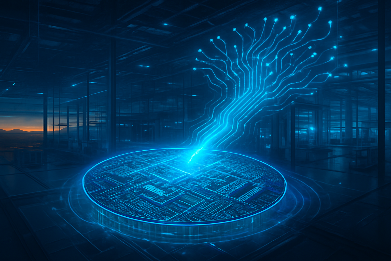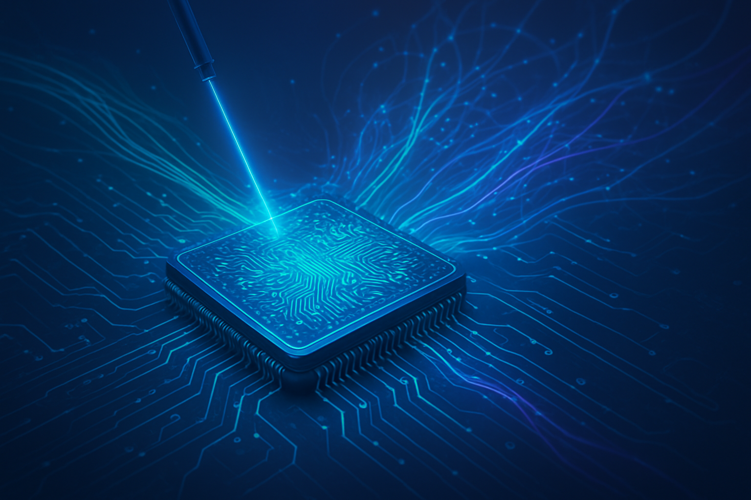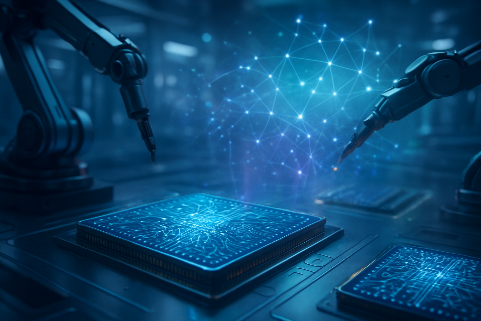
As of January 26, 2026, the semiconductor industry has officially entered a new epoch known as the "Angstrom Era." Taiwan Semiconductor Manufacturing Company (TSM: NYSE) has confirmed that its next-generation 2-nanometer (N2) process technology has successfully moved into high-volume manufacturing, marking a critical milestone for the global technology landscape. With mass production ramping up at the newly completed Hsinchu and Kaohsiung gigafabs, the industry is witnessing the most significant architectural shift in over a decade.
This transition is not merely a routine shrink in transistor size; it represents a fundamental re-engineering of the silicon that powers everything from the smartphones in our pockets to the massive data centers training the next generation of artificial intelligence. With demand for AI compute reaching a fever pitch, TSMC’s N2 node is expected to be the exclusive engine for the world’s most advanced hardware, though industry analysts warn that a massive supply-demand imbalance will likely trigger shortages lasting well into 2027.
The Architecture of the Future: Transitioning to GAA Nanosheets
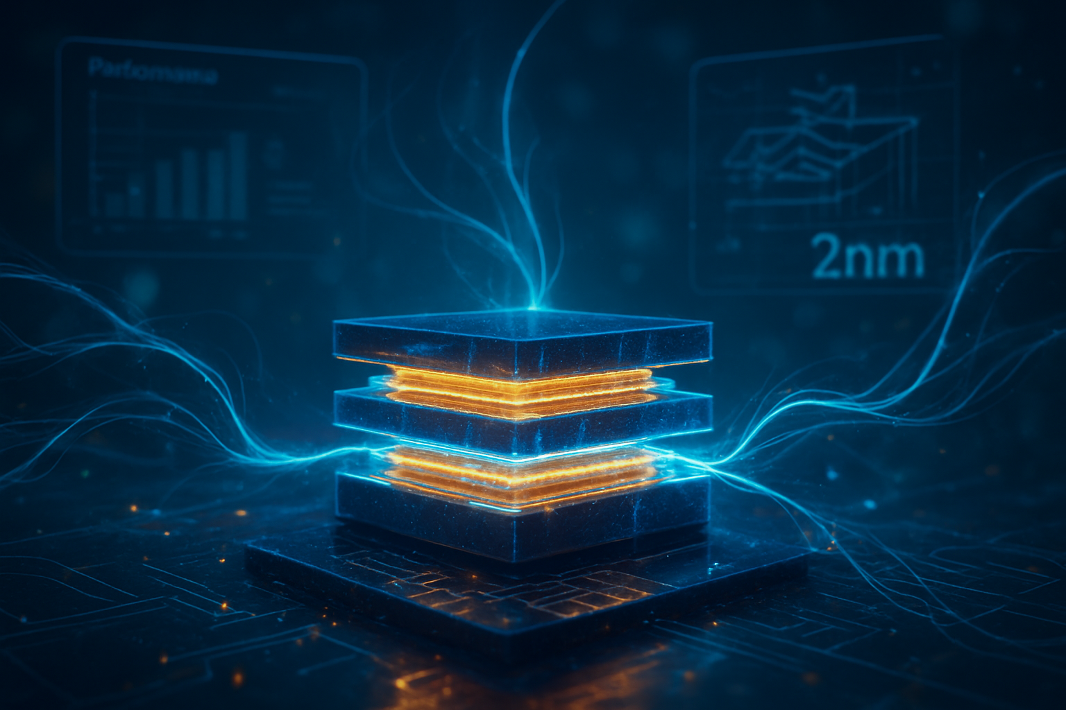
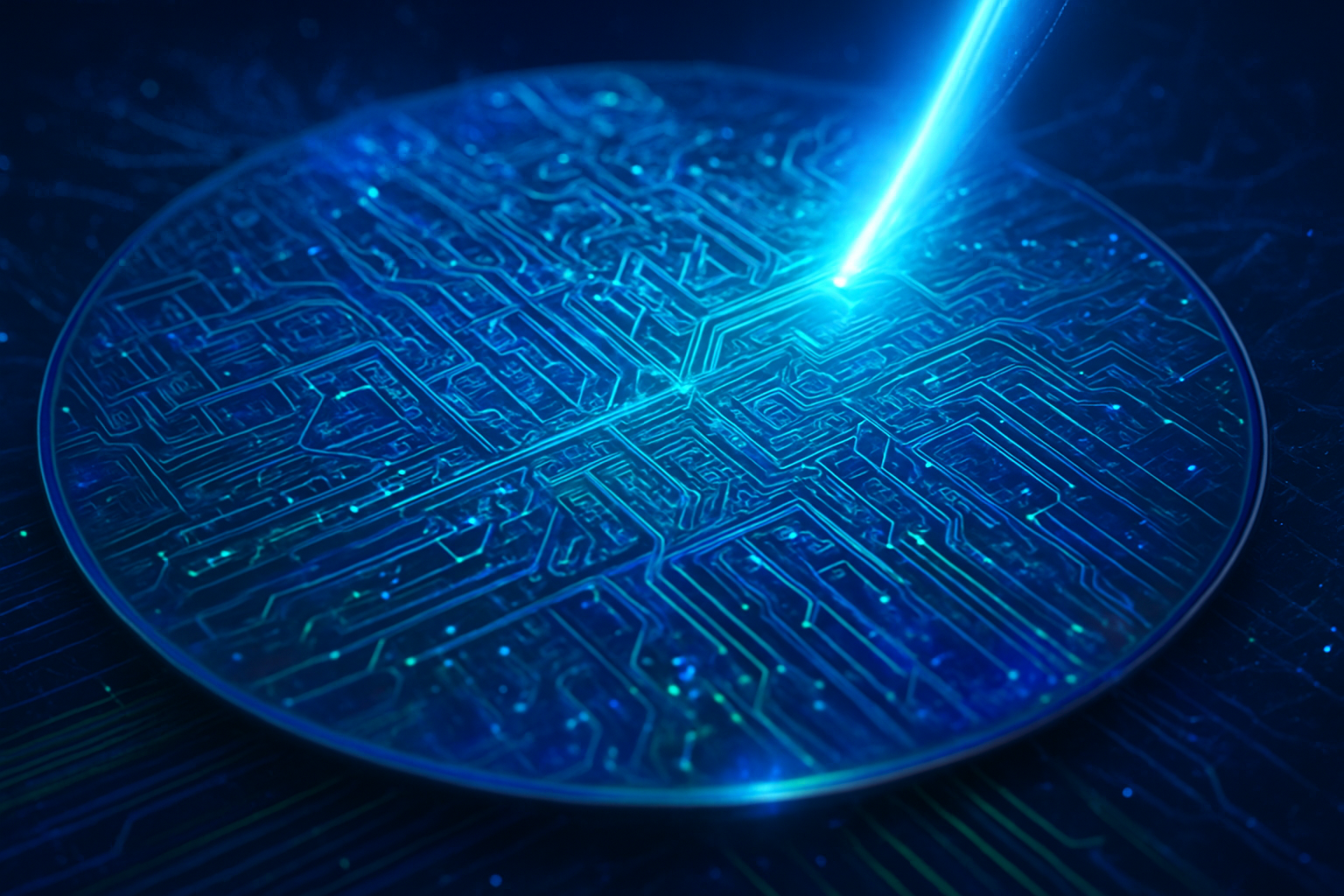
The technical centerpiece of the N2 node is the transition from FinFET (Fin Field-Effect Transistor) architecture to Gate-All-Around (GAA) nanosheet transistors. For the past decade, FinFETs provided the necessary performance gains by using a 3D "fin" structure to control electrical current. However, as transistors approached the physical limits of atomic scales, FinFETs began to suffer from excessive power leakage and diminished efficiency. The new GAA nanosheet design solves this by wrapping the transistor gate entirely around the channel on all four sides, providing superior electrical control and drastically reducing current leakage.
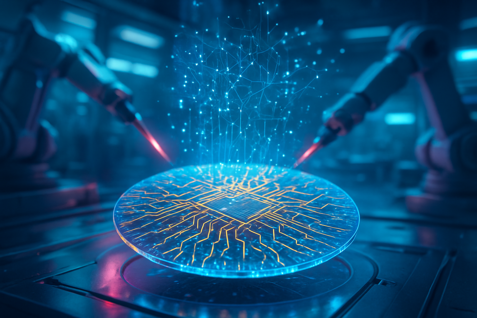
The performance metrics for N2 are formidable. Compared to the previous N3E (3-nanometer) node, the 2nm process offers a 10% to 15% increase in speed at the same power level, or a staggering 25% to 30% reduction in power consumption at the same performance level. Furthermore, the node provides a 15% to 20% increase in logic density. Initial reports from TSMC’s Jan. 15, 2026, earnings call indicate that logic test chip yields for the GAA process have already stabilized between 70% and 80%—a remarkably high figure for a new architecture that suggests TSMC has successfully navigated the "yield valley" that often plagues new process transitions.
Initial reactions from the semiconductor research community have been overwhelmingly positive, with experts noting that the flexibility of nanosheet widths allows designers to optimize specific parts of a chip for either high performance or low power. This level of granular customization was nearly impossible with the fixed-fin heights of the FinFET era, giving chip architects at companies like Apple (AAPL: NASDAQ) and Nvidia (NVDA: NASDAQ) an unprecedented toolkit for the 2026-2027 hardware cycle.
A High-Stakes Race for First-Mover Advantage
The race to secure 2nm capacity has created a strategic divide in the tech industry. Apple remains TSMC’s "alpha" customer, having reportedly booked the lion's share of initial N2 capacity for its upcoming A20 series chips destined for the 2026 iPhone 18 Pro. By being the first to market with GAA-based consumer silicon, Apple aims to maintain its lead in on-device AI and battery efficiency, potentially forcing competitors to wait for second-tier allocations.
Meanwhile, the high-performance computing (HPC) sector is driving even more intense competition. Nvidia’s next-generation "Rubin" (R100) AI architecture is in full production as of early 2026, leveraging N2 to meet the insatiable appetite for Large Language Model (LLM) training. Nvidia has secured over 60% of TSMC’s advanced packaging capacity to support these chips, effectively creating a "moat" that limits the speed at which rivals can scale. Other major players, including Advanced Micro Devices (AMD: NASDAQ) with its Zen 6 architecture and Broadcom (AVGO: NASDAQ), are also in line, though they are grappling with the reality of $30,000-per-wafer price tags—a 50% premium over the 3nm node.
This pricing power solidifies TSMC’s dominance over competitors like Samsung (SSNLF: OTC) and Intel (INTC: NASDAQ). While Intel has made significant strides with its Intel 18A node, TSMC’s proven track record of high-yield volume production has kept the world’s most valuable tech companies within its ecosystem. The sheer cost of 2nm development means that many smaller AI startups may find themselves priced out of the leading edge, potentially leading to a consolidation of AI power among a few "silicon-rich" giants.
The Global Impact: Shortages and the AI Capex Supercycle
The broader significance of the 2nm ramp-up lies in its role as the backbone of the "AI economy." As global data center capacity continues to expand, the efficiency gains of the N2 node are no longer a luxury but a necessity for sustainability. A 30% reduction in power consumption across millions of AI accelerators translates to gigawatts of energy saved, a factor that is becoming increasingly critical as power grids worldwide struggle to support the AI boom.
However, the supply outlook remains precarious. Analysts project that demand for sub-5nm nodes will exceed global capacity by 25% to 30% throughout 2026. This "supply choke" has prompted TSMC to raise its 2026 capital expenditure to a record-breaking $56 billion, specifically to accelerate the expansion of its Baoshan and Kaohsiung facilities. The persistent shortage of 2nm silicon could lead to elongated replacement cycles for smartphones and higher costs for cloud compute services, as the industry enters a period where "performance-per-watt" is the ultimate currency.
The current situation mirrors the semiconductor crunch of 2021, but with a crucial difference: the bottleneck today is not a lack of old-node chips for cars, but a lack of the most advanced silicon for the "brains" of the global economy. This shift underscores a broader trend of technological nationalism, as countries scramble to secure access to the limited 2nm wafers that will dictate the pace of AI innovation for the next three years.
Looking Ahead: The Roadmap to 1.6nm and Backside Power
The N2 node is just the beginning of a multi-year roadmap that TSMC has laid out through 2028. Following the base N2 ramp, the company is preparing for N2P (an enhanced version) and N2X (optimized for extreme performance) to launch in late 2026 and early 2027. The most anticipated advancement, however, is the A16 node—a 1.6nm process scheduled for volume production in late 2026.
A16 will introduce the "Super Power Rail" (SPR), TSMC’s implementation of Backside Power Delivery (BSPDN). By moving the power delivery network to the back of the wafer, designers can free up more space on the front for signal routing, further boosting clock speeds and reducing voltage drop. This technology is expected to be the "holy grail" for AI accelerators, allowing them to push even higher thermal design points without sacrificing stability.
The challenges ahead are primarily thermal and economic. As transistors shrink, managing heat density becomes an existential threat to chip longevity. Experts predict that the move toward 2nm and beyond will necessitate a total rethink of liquid cooling and advanced 3D packaging, which will add further layers of complexity and cost to an already expensive manufacturing process.
Summary of the Angstrom Era
TSMC’s successful ramp of the 2nm N2 node marks a definitive victory in the semiconductor arms race. By successfully transitioning to Gate-All-Around nanosheets and maintaining high yields, the company has secured its position as the indispensable foundry for the AI revolution. Key takeaways from this launch include the massive performance-per-watt gains that will redefine mobile and data center efficiency, and the harsh reality of a "fully booked" supply chain that will keep silicon prices at historic highs.
In the coming months, the industry will be watching for the first 2nm benchmarks from Apple’s A20 and Nvidia’s Rubin architectures. These results will confirm whether the "Angstrom Era" can deliver on its promise to maintain the pace of Moore’s Law or if the physical and economic costs of miniaturization are finally reaching a breaking point. For now, the world’s most advanced AI is being forged in the cleanrooms of Taiwan, and the race to own that silicon has never been more intense.
This content is intended for informational purposes only and represents analysis of current AI developments.
TokenRing AI delivers enterprise-grade solutions for multi-agent AI workflow orchestration, AI-powered development tools, and seamless remote collaboration platforms.
For more information, visit https://www.tokenring.ai/.