Tag: Gallium Nitride

  • Beyond Silicon: How SiC, GaN, and AI are Fueling the 800V Electric Vehicle Revolution

    Beyond Silicon: How SiC, GaN, and AI are Fueling the 800V Electric Vehicle Revolution

    As of January 2026, the electric vehicle (EV) industry has reached a definitive technological tipping point. The era of traditional silicon power electronics is rapidly drawing to a close, replaced by the ascent of Wide-Bandgap (WBG) semiconductors: Silicon Carbide (SiC) and Gallium Nitride (GaN). This transition, once reserved for high-end performance cars, has now moved into the mass market, fundamentally altering the economics of EV ownership by slashing charging times and extending driving ranges to levels previously thought impossible.

    The immediate significance of this shift is being amplified by the integration of artificial intelligence into the semiconductor manufacturing process. In early January 2026, the successful deployment of AI-driven predictive modeling in crystal growth furnaces has allowed manufacturers to scale production to unprecedented levels. These developments are not merely incremental; they represent a total reconfiguration of the EV powertrain, enabling 800-volt architectures to become the new global standard for vehicles priced under $40,000, effectively removing the "range anxiety" and "charging lag" that have historically hindered widespread adoption.

    The 300mm Revolution: Scaling the Wide-Bandgap Frontier

    The technical heart of this revolution lies in the physical properties of SiC and GaN. Unlike traditional silicon, these materials have a wider "energy gap," allowing them to operate at much higher voltages, temperatures, and frequencies. In the traction inverter—the part of the EV that converts DC battery power to AC for the motor—SiC MOSFETs have achieved a staggering 99% efficiency rating in 2026. This efficiency reduces energy loss as heat, allowing for smaller cooling systems and a direct 7% to 10% increase in vehicle range. Meanwhile, GaN has become the dominant material for onboard chargers and DC-DC converters, enabling power densities that allow these components to be reduced in size by nearly 50%.

    The most significant technical milestone of 2026 occurred on January 13, when Wolfspeed (NYSE: WOLF) announced the production of the world’s first 300mm (12-inch) single-crystal SiC wafer. Historically, SiC manufacturing was limited to 150mm or 200mm wafers due to the extreme difficulty of growing large, defect-free crystals. By utilizing AI-enhanced defect detection and thermal gradient control during the growth process, the industry has finally "scaled the yield wall." This 300mm breakthrough is expected to reduce die costs by up to 40%, finally bringing SiC to price parity with legacy silicon components.

    Initial reactions from the research community have been overwhelmingly positive. Analysts at Yole Group have described the 300mm achievement as the "Everest of power electronics," noting that the transition allows for nearly 2.3 times more chips per wafer than the 200mm standard. Industry experts at the Applied Power Electronics Conference (APEC) in January 2026 highlighted that these advancements are no longer just about hardware; they are about "Smart Power." Modern power stages now feature AI-integrated gate drivers that can predict component fatigue months before failure, allowing for predictive maintenance alerts to be delivered directly to the vehicle’s dashboard.

    Market Consolidation and the Strategic AI Pivot

    The semiconductor landscape has undergone significant consolidation to meet the demands of this 800V era. STMicroelectronics (NYSE: STM) has solidified its position as the volume leader, leveraging a fully vertically integrated supply chain. Their Gen-3 SiC MOSFETs are now the standard for mid-market EVs across Europe and Asia. Following a period of financial restructuring in late 2025, Wolfspeed has emerged as a specialized powerhouse, focusing on the high-yield 300mm production that competitors are now racing to emulate.

    The competitive implications are vast for tech giants and startups alike. ON Semiconductor (NASDAQ: ON) has pivoted its strategy toward "EliteSiC" Power Integrated Modules (PIMs), which combine SiC hardware with AI-driven sensing for self-protecting power stages. Meanwhile, Infineon Technologies (OTCMKTS: IFNNY) shocked the market this month by announcing the first high-volume 300mm power GaN production line, a move that positions them to dominate the infrastructure side of the industry, particularly high-speed DC chargers.

    This shift is disrupting the traditional automotive supply chain. Legacy Tier-1 suppliers who failed to pivot to WBG materials are seeing their market share eroded by semiconductor-first companies. Furthermore, the partnership between GaN pioneers and AI leaders like NVIDIA (NASDAQ: NVDA) has created a new category of "AI-Optimized Chargers" that can handle the massive power requirements of both EV fleets and AI data centers, creating a synergistic market that benefits companies at the intersection of energy and computation.

    The Decarbonization Catalyst: From Infrastructure to Grid Intelligence

    Beyond the vehicle itself, the move to SiC and GaN is a critical component of the broader global energy transition. The democratization of 800V systems has paved the way for "Ultra-Fast" charging networks. In 2025, BYD (OTCMKTS: BYDDF) released its Super e-Platform, and by January 2026, it has demonstrated the ability to add 400km of range in just five minutes using SiC-based megawatt chargers. This capability brings the EV refueling experience into direct competition with internal combustion engine (ICE) vehicles, removing the final psychological barrier for many consumers.

    However, this rapid charging capability places immense strain on local electrical grids. This is where AI-driven grid intelligence becomes essential. By using AI to orchestrate the "handshake" between the SiC power modules in the car and the GaN-based power stages in the charger, utility companies can balance loads in real-time. This "Smart Power" landscape allows for bidirectional charging (V2G), where EVs act as a distributed battery for the grid, discharging energy during peak demand and charging when renewable energy is most abundant.

    The impact of this development is comparable to the introduction of the lithium-ion battery itself. While the battery provides the storage, SiC and GaN provide the "vascular system" that allows that energy to flow efficiently. Some concerns remain regarding the environmental impact of SiC wafer production, which is energy-intensive. However, the 20% yield boost provided by AI manufacturing has already begun to lower the carbon footprint per chip, making the entire lifecycle of the EV significantly greener than models from just three years ago.

    The Roadmap to 2030: 1200V Architectures and Beyond

    Looking ahead, the next frontier is already visible on the horizon: 1200V architectures. While 800V is the current benchmark for 2026, high-performance trucks, delivery vans, and heavy-duty equipment are expected to migrate toward 1200V by 2028. This will require even more advanced SiC formulations and potentially the introduction of "Diamond" semiconductors, which offer even wider bandgaps than SiC.

    In the near term, expect to see the "miniaturization" of the drivetrain. As AI continues to optimize switching frequencies, we will likely see "all-in-one" drive units where the motor, inverter, and gearbox are integrated into a single, compact module no larger than a carry-on suitcase. Challenges remain in the global supply of raw materials like high-purity carbon and gallium, but experts predict that the opening of new domestic refining facilities in North America and Europe by 2027 will alleviate these bottlenecks.

    The integration of solid-state batteries, expected to hit the market in limited volumes by late 2027, will further benefit from SiC power electronics. The high thermal stability of SiC is a perfect match for the higher operating temperatures of some solid-state chemistries. Experts predict that the combination of SiC/GaN power stages and solid-state batteries will lead to "thousand-mile" EVs by the end of the decade.

    Conclusion: The New Standard of Electric Mobility

    The shift to Silicon Carbide and Gallium Nitride, supercharged by AI manufacturing and real-time power management, represents the most significant advancement in EV technology this decade. As of January 2026, we have moved past the "early adopter" phase and into an era where electric mobility is defined by efficiency, speed, and intelligence. The 300mm wafer breakthrough and the 800V standard have effectively leveled the playing field between electric and gasoline vehicles.

    For the tech industry and society at large, the key takeaway is that the "silicon" in Silicon Valley is no longer the only game in town. The future of energy is wide-bandgap. In the coming weeks, watch for further announcements from Tesla (NASDAQ: TSLA) regarding their next-generation "Unboxed" manufacturing process, which is rumored to rely heavily on the new AI-optimized SiC modules. The road to 2030 is electric, and it is being paved with SiC and GaN.


    This content is intended for informational purposes only and represents analysis of current AI developments.

    TokenRing AI delivers enterprise-grade solutions for multi-agent AI workflow orchestration, AI-powered development tools, and seamless remote collaboration platforms.
    For more information, visit https://www.tokenring.ai/.
  • The Power Behind the Intelligence: Wide-Bandgap Semiconductors to Top $5 Billion in 2026 as AI and EVs Converge

    The Power Behind the Intelligence: Wide-Bandgap Semiconductors to Top $5 Billion in 2026 as AI and EVs Converge

    The global semiconductor landscape is witnessing a seismic shift as 2026 marks the definitive "Wide-Bandgap (WBG) Era." Driven by the insatiable power demands of AI data centers and the wholesale transition of the automotive industry toward high-voltage architectures, the market for Silicon Carbide (SiC) and Gallium Nitride (GaN) discrete devices is projected to exceed $5.3 billion this year. This milestone represents more than just a fiscal achievement; it signals the end of silicon’s decades-long dominance in high-power applications, where its thermal and electrical limits have finally been reached by the sheer scale of modern computing.

    As of late January 2026, the industry is tracking a massive capacity build-out, with major manufacturers racing to bring new fabrication plants online. This surge is largely fueled by the realization that current AI hardware, despite its logical brilliance, is physically constrained by heat. By replacing traditional silicon with WBG materials, engineers are finding they can manage the immense thermal output of next-generation GPU clusters and EV inverters with unprecedented efficiency, effectively doubling down on the performance-per-watt metrics that now dictate market leadership.

    Technical Superiority and the Rise of the 8-Inch Wafer

    The technical transition at the heart of this growth centers on the physical properties of SiC and GaN compared to traditional Silicon (Si). Silicon Carbide boasts a thermal conductivity nearly 3.3 times higher than silicon, allowing it to dissipate heat far more effectively and operate at temperatures exceeding 200°C. Meanwhile, GaN’s superior electron mobility allows for switching frequencies in the megahertz range—significantly higher than silicon—which enables the use of much smaller passive components like inductors and capacitors. These properties are no longer just "nice-to-have" advantages; they are essential for the 800V Direct Current (DC) architectures now becoming the standard in both high-end electric vehicles and AI server racks.

    A cornerstone of the 2026 market expansion is the massive investment by ROHM Semiconductor ([TYO: 6963]). The company’s new Miyazaki Plant No. 2, a sprawling 230,000 m² facility, has officially entered its high-volume phase this year. This plant is a critical hub for the production of 8-inch (200mm) SiC substrates. Moving from 6-inch to 8-inch wafers is a technical hurdle that has historically plagued the industry, but the successful scaling at the Miyazaki and Chikugo plants has increased chip output per wafer by nearly 1.8x. This efficiency gain has been instrumental in driving down the cost of SiC devices, making them competitive with silicon-based Insulated Gate Bipolar Transistors (IGBTs) for the first time in mid-market applications.

    Initial reactions from the semiconductor research community have highlighted how these advancements solve the "thermal bottleneck" of modern AI. Recent tests of SiC-based power stages in server PSUs (Power Supply Units) have demonstrated peak efficiencies of 98%, a leap from the 94% ceiling typical of silicon. In the world of hyperscale data centers, that 4% difference translates into millions of dollars in saved electricity and cooling costs. Furthermore, NVIDIA ([NASDAQ: NVDA]) has reportedly begun exploring SiC interposers for its newest Blackwell-successor chips, aiming to reduce GPU operating temperatures by up to 20°C, which significantly extends the lifespan of the hardware under 24/7 AI training loads.

    Corporate Maneuvering and Market Positioning

    The surge in WBG demand has created a clear divide between companies that secured their supply chains early and those now scrambling for capacity. STMicroelectronics ([NYSE: STM]) and Infineon Technologies ([ETR: IFX]) continue to hold dominant positions, but the aggressive expansion of ROHM and Wolfspeed ([NYSE: WOLF]) has intensified the competitive landscape. These companies are no longer just component suppliers; they are strategic partners for the world’s largest tech and automotive giants. For instance, BYD ([HKG: 1211]) and Hyundai Motor Company ([KRX: 005380]) have integrated SiC into their 2026 vehicle lineups to achieve a 5-10% range increase without increasing battery size, a move that provides a massive competitive edge in the price-sensitive EV market.

    In the data center space, the impact is equally transformative. Major cloud providers are shifting toward 800V high-voltage direct current architectures to power their AI clusters. This has benefited companies like Lucid Motors ([NASDAQ: LCID]), which has leveraged its expertise in high-voltage power electronics to consult on industrial power management. The strategic advantage now lies in "vertical integration"—those who control the substrate production (the raw SiC or GaN material) are less vulnerable to the price volatility and shortages that defined the early 2020s.

    Wider Significance: Energy, AI, and Global Sustainability

    The transition to WBG semiconductors represents a critical pivot in the global AI landscape. As concerns grow regarding the environmental impact of AI—specifically the massive energy consumption of large language model (LLM) training—SiC and GaN offer a tangible path toward "Greener AI." By reducing switching losses and improving thermal management, these materials are estimated to reduce the carbon footprint of a 10MW data center by nearly 15% annually. This aligns with broader ESG goals while simultaneously allowing companies to pack more compute power into the same physical footprint.

    However, the rapid growth also brings potential concerns, particularly regarding the complexity of the manufacturing process. SiC crystals are notoriously difficult to grow, requiring temperatures near 2,500°C and specialized furnaces. Any disruption in the supply of high-purity graphite or specialized silicon carbide powder could create a bottleneck that slows the deployment of AI infrastructure. Comparisons are already being made to the 2021 chip shortage, with analysts warning that the "Power Gap" might become the next "Memory Gap" in the tech industry’s race toward artificial general intelligence.

    The Horizon: 12-Inch Wafers and Ultra-Fast Charging

    Looking ahead, the industry is already eyeing the next frontier: 12-inch (300mm) SiC production. While 8-inch wafers are the current state-of-the-art in 2026, R&D labs at ROHM and Wolfspeed are reportedly making progress on larger formats that could further slash costs by 2028. We are also seeing the rise of "GaN-on-SiC" and "GaN-on-GaN" technologies, which aim to combine the high-frequency benefits of Gallium Nitride with the superior thermal dissipation of Silicon Carbide for ultra-dense AI power modules.

    On the consumer side, the proliferation of these materials will soon manifest in 350kW+ ultra-fast charging stations, capable of charging an EV to 80% in under 10 minutes without overheating. Experts predict that by 2027, the use of WBG semiconductors will be so pervasive that traditional silicon power devices will be relegated to low-power, "legacy" electronics. The primary challenge remains the development of standardized testing protocols for these materials, as their long-term reliability in the extreme environments of an AI server or a vehicle drivetrain is still being documented in real-time.

    Conclusion: A Fundamental Shift in Power

    The 2026 milestone of a $5 billion market for SiC and GaN discrete devices marks a fundamental shift in how we build the world’s most advanced machines. From the silicon-carbide-powered inverters in our cars to the gallium-nitride-cooled servers processing our queries, WBG materials have moved from a niche laboratory curiosity to the backbone of the global digital and physical infrastructure.

    As we move through the remainder of 2026, the key developments to watch will be the output yield of ROHM’s Miyazaki plant and the potential for a "Power-Efficiency War" between AI labs. In a world where intelligence is limited by the power you can provide and the heat you can remove, the masters of wide-bandgap semiconductors may very well hold the keys to the future of AI development.


    This content is intended for informational purposes only and represents analysis of current AI developments.

    TokenRing AI delivers enterprise-grade solutions for multi-agent AI workflow orchestration, AI-powered development tools, and seamless remote collaboration platforms.
    For more information, visit https://www.tokenring.ai/.

  • The Silent Revolution: How SiC and GaN are Powering the AI Infrastructure and EV Explosion

    The Silent Revolution: How SiC and GaN are Powering the AI Infrastructure and EV Explosion

    As of December 24, 2025, the semiconductor industry has reached a historic inflection point. The "Energy Wall"—a term coined by researchers to describe the physical limits of traditional silicon in high-power applications—has finally been breached. In its place, Wide-Bandgap (WBG) semiconductors, specifically Silicon Carbide (SiC) and Gallium Nitride (GaN), have emerged as the foundational pillars of the modern digital and automotive economy. These materials are no longer niche technologies for specialized hardware; they are now the essential components enabling the massive power demands of generative AI data centers and the 800-volt charging speeds of the latest electric vehicles (EVs).

    The significance of this transition cannot be overstated. With next-generation AI accelerators now drawing upwards of 2 kilowatts per package, the efficiency losses associated with legacy silicon-based power systems have become unsustainable. By leveraging the superior physical properties of SiC and GaN, engineers have managed to shrink power supply units by 50% while simultaneously slashing energy waste. This shift is effectively decoupling the growth of AI compute from the exponential rise in energy consumption, providing a critical lifeline for a power-hungry industry.

    Breaking the Silicon Ceiling: The Rise of 200mm and 300mm WBG

    The technical superiority of WBG materials lies in their "bandgap"—the energy required for electrons to move from the valence band to the conduction band. Traditional silicon has a bandgap of approximately 1.1 electron volts (eV), whereas SiC and GaN boast bandgaps of 3.2 eV and 3.4 eV, respectively. This allows these materials to operate at much higher voltages, temperatures, and frequencies without breaking down. In late 2025, the industry has successfully transitioned to 200mm (8-inch) SiC wafers, a move led by STMicroelectronics (NYSE: STM) at its Catania "Silicon Carbide Campus." This transition has increased chip yield per wafer by over 50%, finally bringing the cost of SiC closer to that of high-end silicon.

    Furthermore, 2025 has seen the commercial debut of Vertical GaN (vGaN), a breakthrough spearheaded by onsemi (NASDAQ: ON). Unlike traditional lateral GaN, which conducts current across the surface of the chip, vGaN conducts current through the substrate. This allows GaN to compete directly with SiC in the 1200V range, making it suitable for the heavy-duty traction inverters found in electric trucks and industrial machinery. Meanwhile, Infineon Technologies (OTC: IFNNY) has begun sampling the world’s first 300mm GaN-on-Silicon wafers, a feat that promises to revolutionize the economics of power electronics by leveraging existing high-volume silicon manufacturing lines.

    These advancements differ from previous technologies by offering a "triple threat" of benefits: higher switching frequencies, lower on-resistance, and superior thermal conductivity. In practical terms, this means that power converters can use smaller capacitors and inductors, leading to more compact and lightweight designs. Industry experts have lauded these developments as the most significant change in power electronics since the invention of the MOSFET in the 1960s, noting that the "Silicon-only" era of power management is effectively over.

    Market Dominance and the AI Power Supply Gold Rush

    The shift toward WBG materials has triggered a massive realignment among semiconductor giants. STMicroelectronics (NYSE: STM) currently holds a commanding 29% share of the SiC market, largely due to its long-standing partnership with major EV manufacturers and its early investment in 200mm production. However, onsemi (NASDAQ: ON) has rapidly closed the gap, securing multi-billion dollar long-term supply agreements with automotive OEMs and emerging as the leader in the newly formed vGaN segment.

    The AI data center market has become the new primary battleground for these companies. As hyperscalers like Amazon and Google deploy 12kW Power Supply Units (PSUs) to support the latest AI clusters, the demand for GaN has skyrocketed. These PSUs, which utilize SiC for high-voltage AC-DC conversion and GaN for high-frequency DC-DC switching, achieve 98% efficiency. This is a critical metric for data center operators, as every 1% increase in efficiency can save millions of dollars in electricity and cooling costs annually.

    The competitive landscape has also seen dramatic shifts for legacy players. Wolfspeed (NYSE: WOLF), once the pure-play leader in SiC, emerged from a successful Chapter 11 restructuring in September 2025. With its Mohawk Valley Fab finally reaching 30% utilization, the company is stabilizing its supply chain and refocusing on high-purity SiC substrates, where it still holds a 33% global market share. This restructuring has allowed Wolfspeed to remain a vital supplier to other chipmakers while shedding the debt that hampered its growth during the 2024 downturn.

    Societal Impact: Efficiency as the New Sustainability

    The broader significance of the WBG revolution extends far beyond corporate balance sheets; it is a critical component of global sustainability efforts. In the EV sector, the adoption of 800V architectures enabled by SiC has virtually eliminated "range anxiety" for the average consumer. By allowing for 15-minute "flash charging" and increasing vehicle range by 7-10% without increasing battery size, WBG materials are making EVs more practical and affordable for the mass market.

    In the realm of AI, WBG semiconductors are solving the "PUE Crisis" (Power Usage Effectiveness). By reducing the heat generated during power conversion, these materials have lowered the energy demand of data center cooling systems by an estimated 40%. This allows AI companies to pack more compute density into existing facilities, delaying the need for costly new grid connections and reducing the environmental footprint of large language model training.

    However, the rapid transition has not been without concerns. The concentration of SiC substrate production remains a geopolitical flashpoint, with Chinese players like SICC and Tankeblue aggressively gaining market share and undercutting Western prices. This has led to increased calls for "local-for-local" supply chains to ensure that the critical infrastructure of the AI era is not vulnerable to trade disruptions.

    The Horizon: Ultra-Wide Bandgap and AI-Optimized Power

    Looking ahead to 2026 and beyond, the industry is already eyeing the next frontier: Ultra-Wide Bandgap (UWBG) materials. Research into Gallium Oxide and Diamond-based semiconductors is accelerating, with the goal of creating chips that can handle even higher voltages and temperatures than SiC. These materials could eventually power the next generation of orbital satellites and deep-sea exploration equipment, where environmental conditions are too extreme for current technology.

    Another burgeoning field is "Cognitive Power Electronics." Tesla recently revealed a system that uses real-time AI to adjust SiC switching frequencies based on driving conditions and battery state-of-health. This software-defined approach to power management allows for a 75% reduction in SiC content while maintaining the same level of performance, potentially lowering the cost of entry-level EVs. Experts predict that this marriage of AI and WBG hardware will become the standard for all high-performance energy systems by the end of the decade.

    A New Era for Energy and Intelligence

    The transition to Silicon Carbide and Gallium Nitride represents a fundamental shift in how humanity manages energy. By moving past the physical limitations of silicon, the semiconductor industry has provided the necessary infrastructure to support the dual revolutions of artificial intelligence and electrified transportation. The developments of 2025 have proven that efficiency is not just a secondary goal, but a primary enabler of technological progress.

    As we move into 2026, the key metrics to watch will be the continued scaling of 300mm GaN production and the integration of AI-driven material discovery to further enhance chip reliability. The "Silent Revolution" of WBG semiconductors may not always capture the headlines like the latest AI model, but it is the indispensable engine driving the future of innovation.


    This content is intended for informational purposes only and represents analysis of current AI developments.

    TokenRing AI delivers enterprise-grade solutions for multi-agent AI workflow orchestration, AI-powered development tools, and seamless remote collaboration platforms.
    For more information, visit https://www.tokenring.ai/.

  • The Efficiency Frontier: How AI-Driven Silicon Carbide and Gallium Nitride are Redefining the Electric Vehicle

    The Efficiency Frontier: How AI-Driven Silicon Carbide and Gallium Nitride are Redefining the Electric Vehicle

    The global automotive industry has reached a pivotal inflection point as of late 2025, driven by a fundamental shift in the materials that power our vehicles. The era of traditional silicon-based power electronics is rapidly drawing to a close, replaced by a new generation of "wide-bandgap" (WBG) semiconductors: Silicon Carbide (SiC) and Gallium Nitride (GaN). This transition is not merely a hardware upgrade; it is a sophisticated marriage of advanced material science and artificial intelligence that is enabling the 800-volt architectures and 500-mile ranges once thought impossible for mass-market electric vehicles (EVs).

    This technological leap comes at a critical time. As of December 22, 2025, the EV market has shifted its focus from raw battery capacity to "efficiency-first" engineering. By utilizing AI-optimized SiC and GaN components, automakers are achieving up to 99% inverter efficiency, effectively adding 30 to 50 miles of range to vehicles without increasing the size—or the weight—of the battery pack. This "silent revolution" in the drivetrain is what finally allows EVs to achieve price and performance parity with internal combustion engines across all vehicle segments.

    The Physics of Performance: Breaking the Silicon Ceiling

    The technical superiority of SiC and GaN stems from their wide bandgap—a physical property that allows these materials to operate at much higher voltages, temperatures, and frequencies than standard silicon. While traditional silicon has a bandgap of approximately 1.1 electron volts (eV), SiC sits at 3.3 eV and GaN at 3.4 eV. In practical terms, this means these semiconductors can withstand electric fields ten times stronger than silicon, allowing for thinner device layers and significantly lower internal resistance.

    In late 2025, the industry has standardized around 800V architectures, a move made possible by these materials. High-voltage systems allow for thinner wiring—reducing vehicle weight—and enable "ultra-fast" charging sessions that can replenish 80% of a battery in under 15 minutes. Furthermore, the higher switching frequencies of GaN, which can now reach the megahertz range in traction inverters, allow for much smaller passive components like inductors and capacitors. This has led to the "shrinking" of the power electronics block; a 2025-model traction inverter is roughly 40% smaller and 50% lighter than its 2021 predecessor.

    The integration of AI has been the "secret sauce" in mastering these difficult-to-manufacture materials. Throughout 2025, companies like Infineon Technologies (OTCMKTS: IFNNY) have utilized Convolutional Neural Networks (CNNs) to achieve a breakthrough in 300mm GaN-on-Silicon manufacturing. By using AI-driven defect classification, Infineon has reached 99% accuracy in identifying nanoscale lattice mismatches during the epitaxy process, a feat that was previously the primary bottleneck to mass-market GaN adoption. Initial reactions from the research community suggest that this 300mm milestone will drop the cost of GaN power chips by nearly 50% by the end of 2026.

    Market Dynamics: A New Hierarchy of Power

    The shift to WBG semiconductors has fundamentally reshaped the competitive landscape for chipmakers and OEMs alike. STMicroelectronics (NYSE: STM) currently maintains the largest market share in the SiC space, largely due to its long-standing partnership with Tesla (NASDAQ: TSLA). However, the market saw a massive shakeup in mid-2025 when Wolfspeed (NYSE: WOLF) emerged from a strategic Chapter 11 restructuring. Now operating as a "pure-play" SiC powerhouse, Wolfspeed has pivoted its focus toward 200mm wafer production at its Mohawk Valley fab, recently securing a massive multi-year supply agreement with Toyota for their next-generation e-mobility platforms.

    Meanwhile, ON Semiconductor (NASDAQ: ON), under its EliteSiC brand, has aggressively captured the Asian market. Their recent partnership with Xiaomi for the YU7 SUV highlights a growing trend: the "Vertical GaN" (vGaN) breakthrough. By using AI to optimize the vertical structure of GaN crystals, ON Semi has created chips that handle the high-power loads of heavy SUVs—a domain previously reserved exclusively for SiC. This creates a new competitive front between SiC and GaN, potentially disrupting the established product roadmaps of major power electronics suppliers.

    Tesla, ever the industry disruptor, has taken a different strategic path. In late 2025, the company revealed it has successfully reduced the SiC content in its "Next-Gen" platform by 75% without sacrificing performance. This was achieved through "Cognitive Power Electronics"—an AI-driven gate driver system that uses real-time machine learning to adjust switching frequencies based on driving conditions. This software-centric approach allows Tesla to use fewer, smaller chips, giving them a significant cost advantage over legacy manufacturers who are still reliant on high volumes of raw WBG material.

    The AI Connection: From Material Discovery to Real-Time Management

    The significance of the SiC and GaN transition extends far beyond the hardware itself; it represents the first major success of AI-driven material science. Throughout 2024 and 2025, researchers have utilized Neural Network Potentials (NNPs), such as the PreFerred Potential (PFP) model, to simulate atomic interactions in semiconductor substrates. This AI-led approach accelerated the discovery of new high-k dielectrics for SiC MOSFETs, a process that would have taken decades using traditional trial-and-error laboratory methods.

    Beyond the factory floor, AI is now embedded directly into the vehicle's power management system. Modern Battery Management Systems (BMS), such as those found in the 2025 Hyundai (OTCMKTS: HYMTF) IONIQ 5, use Recurrent Neural Networks (RNNs) to monitor the "State of Health" (SOH) of individual power transistors. These systems can predict a semiconductor failure up to three months in advance by analyzing subtle deviations in thermal signatures and switching transients. This "predictive maintenance" for the drivetrain is a milestone that mirrors the evolution of jet engine monitoring in the aerospace industry.

    However, this transition is not without concerns. The reliance on complex AI models to manage high-voltage power electronics introduces new cybersecurity risks. Industry experts have warned that a "malicious firmware update" targeting the AI-driven gate drivers could theoretically cause a catastrophic failure of the inverter. As a result, 2025 has seen a surge in "Secure-BMS" startups focusing on hardware-level encryption for the data streams flowing between the battery cells and the WBG power modules.

    The Road Ahead: 2026 and Beyond

    Looking toward 2026, the industry expects the "GaN-ification" of the on-board charger (OBC) and DC-DC converter to be nearly 100% complete in new EV models. The next frontier is the integration of WBG materials into wireless charging pads. AI models are currently being trained to manage the complex electromagnetic fields required for high-efficiency wireless power transfer, with initial 11kW systems expected to debut in premium German EVs by late next year.

    The primary challenge remaining is the scaling of 300mm manufacturing. While Infineon has proven the concept, the capital expenditure required to transition the entire industry away from 150mm and 200mm lines is immense. Experts predict a "two-tier" market for the next few years: premium vehicles utilizing AI-optimized 300mm GaN and SiC for maximum efficiency, and budget EVs utilizing "hybrid inverters" that mix traditional silicon IGBTs with small amounts of SiC to balance cost.

    Furthermore, as AI compute loads within the vehicle increase—driven by Level 4 autonomous driving systems—the power demand of the "AI brain" itself is becoming a factor. In late 2025, NVIDIA (NASDAQ: NVDA) and MediaTek announced a joint venture to develop WBG-based power delivery modules specifically for AI chips, ensuring that the energy saved by the SiC drivetrain isn't immediately consumed by the car's self-driving computer.

    A New Foundation for Electrification

    The transition to Silicon Carbide and Gallium Nitride marks the end of the "experimental" phase of electric mobility. By leveraging the unique physical properties of these wide-bandgap materials and the predictive power of artificial intelligence, the automotive industry has solved the twin problems of range anxiety and slow charging. The developments of 2025 have proven that the future of the EV is not just about bigger batteries, but about smarter, more efficient power conversion.

    In the history of AI, this period will likely be remembered as the moment when artificial intelligence moved from the "cloud" to the "core" of physical infrastructure. The ability to design, manufacture, and manage power at the atomic level using machine learning has fundamentally changed our relationship with energy. As we move into 2026, the industry will be watching closely to see if the cost reductions promised by 300mm manufacturing can finally bring $25,000 high-performance EVs to the global mass market.

    For now, the message is clear: the silicon age of the automobile is over. The WBG era, powered by AI, has begun.


    This content is intended for informational purposes only and represents analysis of current AI developments.

    TokenRing AI delivers enterprise-grade solutions for multi-agent AI workflow orchestration, AI-powered development tools, and seamless remote collaboration platforms.
    For more information, visit https://www.tokenring.ai/.

  • The Power Behind the Pulse: How SiC and GaN Are Breaking AI’s ‘Energy Wall’ in 2025

    The Power Behind the Pulse: How SiC and GaN Are Breaking AI’s ‘Energy Wall’ in 2025

    As we close out 2025, the semiconductor industry has reached a critical inflection point where the limitations of traditional silicon are no longer just a technical hurdle—they are a threat to the scaling of artificial intelligence. To keep pace with the massive energy demands of next-generation AI clusters and 800V electric vehicle (EV) architectures, the market has decisively shifted toward Wide Bandgap (WBG) materials. Silicon Carbide (SiC) and Gallium Nitride (GaN) have transitioned from niche "specialty" components to the foundational infrastructure of the modern digital economy, enabling power densities that were thought impossible just three years ago.

    The significance of this development cannot be overstated: by late 2025, the "energy wall"—the point at which power delivery and heat dissipation limit AI performance—has been breached. This breakthrough is driven by the massive industrial pivot toward 200mm (8-inch) SiC manufacturing and the emergence of 300mm (12-inch) GaN-on-Silicon technologies. These advancements have slashed costs and boosted yields, allowing hyperscalers and automotive giants to integrate high-efficiency power stages directly into their most advanced hardware.

    The Technical Frontier: 200mm Wafers and Vertical GaN

    The technical narrative of 2025 is dominated by the industry-wide transition to 200mm SiC wafers. This shift has provided a roughly 20% reduction in die cost while increasing the number of chips per wafer by 80%. Leading the charge in technical specifications, the industry has moved beyond 150mm legacy lines to support 12kW Power Supply Units (PSUs) for AI data centers. These units, which leverage a combination of SiC for high-voltage AC-DC conversion and GaN for high-frequency DC-DC switching, now achieve the "80 PLUS Titanium" efficiency standard, reaching 96-98% efficiency. This reduces heat waste by nearly 50% compared to the silicon-based units of 2022.

    Perhaps the most significant technical advancement of the year is the commercial launch of Vertical GaN (vGaN). Pioneered by companies like onsemi (NASDAQ:ON), vGaN differs from traditional lateral GaN by conducting current through the substrate. This allows it to compete directly with SiC in the 800V to 1200V range, offering the high switching speeds of GaN with the ruggedness of SiC. Meanwhile, Infineon Technologies (OTC:IFNNY) has stunned the research community by successfully shipping the first 300mm GaN-on-Silicon wafers, which yield 2.3 times more chips than the 200mm standard, effectively bringing GaN closer to cost parity with traditional silicon.

    Market Dynamics: Restructuring and Global Expansion

    The business landscape for WBG semiconductors has undergone a dramatic transformation in 2025. Wolfspeed (NYSE:WOLF), once struggling with debt and manufacturing delays, emerged from Chapter 11 bankruptcy in September 2025 as a leaner, restructured entity. Its Mohawk Valley Fab has finally reached 30% utilization, supplying critical SiC components to major automotive partners like Toyota (NYSE:TM) and Lucid (NASDAQ:LCID). This turnaround has stabilized the SiC supply chain, providing a reliable alternative to the diversifying European giants.

    In Europe, STMicroelectronics (NYSE:STM) has solidified its dominance in the automotive sector with the full-scale operation of its Catania Silicon Carbide Campus in Italy. This facility is the first of its kind to integrate the entire supply chain—from substrate growth to back-end module assembly—on a single site. Simultaneously, onsemi is expanding its footprint with a €1.6 billion facility in the Czech Republic, supported by EU grants. These strategic moves are designed to counter the rising tide of China-based substrate manufacturers, such as SICC and Tankeblue, which now command a 35% market share in SiC substrates, triggering the first real price wars in the WBG sector.

    AI Data Centers: The New Growth Engine

    While EVs were the initial catalyst for SiC, the explosion of AI infrastructure has become the primary driver for GaN and SiC growth in late 2025. Systems like the NVIDIA (NASDAQ:NVDA) Blackwell and its successors require unprecedented levels of power density. The transition to 800V DC power distribution at the rack level mirrors the 800V transition in EVs, creating a massive cross-sector synergy. WBG materials allow for smaller, more efficient DC-DC converters that sit closer to the GPU, minimizing "line loss" and allowing data centers to reduce cooling costs by an estimated 40%.

    This shift has broader implications for global sustainability. As AI energy consumption becomes a political and environmental flashpoint, the adoption of SiC and GaN is being framed as a "green" imperative. Regulatory bodies in the EU and North America have begun mandating higher efficiency standards for data centers, effectively making WBG semiconductors a legal requirement for new builds. This has created a "moat" for companies like Infineon and STM, whose advanced modules are the only ones capable of meeting these stringent new 2025 benchmarks.

    The Horizon: 300mm Scaling and Chip-Level Integration

    Looking ahead to 2026 and beyond, the industry is preparing for the "commoditization of SiC." As 200mm capacity becomes the global standard, experts predict a significant drop in prices, which will accelerate the adoption of SiC in mid-range and budget EVs. The next frontier is the full scaling of 300mm GaN-on-Silicon, which will likely push GaN into consumer electronics beyond just chargers, potentially entering the power stages of laptops and home appliances to further reduce global energy footprints.

    Furthermore, we are seeing the early stages of "integrated power-on-chip" designs. Research labs are experimenting with growing GaN layers directly onto silicon logic wafers. If successful, this would allow power management to be integrated directly into the AI processor itself, further reducing latency and energy loss. Challenges remain, particularly regarding the lattice mismatch between different materials, but the progress made in 2025 suggests these hurdles are surmountable within the next three to five years.

    Closing the Loop on the 2025 Power Revolution

    The state of the semiconductor market in late 2025 confirms that the era of "Silicon Only" is over. Silicon Carbide has claimed its crown in the high-voltage automotive and industrial sectors, while Gallium Nitride is rapidly conquering the high-frequency world of AI data centers and consumer tech. The successful transition to 200mm manufacturing and the emergence of 300mm GaN have provided the economies of scale necessary to fuel the next decade of technological growth.

    As we move into 2026, the key metrics to watch will be the pace of China’s substrate expansion and the speed at which vGaN can challenge SiC’s 1200V dominance. For now, the integration of these advanced materials has successfully averted an energy crisis in the AI sector, proving once again that the most profound revolutions in computing often happen in the quiet, high-voltage world of power electronics.


    This content is intended for informational purposes only and represents analysis of current AI developments.

    TokenRing AI delivers enterprise-grade solutions for multi-agent AI workflow orchestration, AI-powered development tools, and seamless remote collaboration platforms.
    For more information, visit https://www.tokenring.ai/.

  • GaN: The Unsung Hero Powering AI’s Next Revolution

    GaN: The Unsung Hero Powering AI’s Next Revolution

    The relentless march of Artificial Intelligence (AI) demands ever-increasing computational power, pushing the limits of traditional silicon-based hardware. As AI models grow in complexity and data centers struggle to meet escalating energy demands, a new material is stepping into the spotlight: Gallium Nitride (GaN). This wide-bandgap semiconductor is rapidly emerging as a critical component for more efficient, powerful, and compact AI hardware, promising to unlock technological breakthroughs that were previously unattainable with conventional silicon. Its immediate significance lies in its ability to address the pressing challenges of power consumption, thermal management, and physical footprint that are becoming bottlenecks for the future of AI.

    The Technical Edge: How GaN Outperforms Silicon for AI

    GaN's superiority over traditional silicon in AI hardware stems from its fundamental material properties. With a bandgap of 3.4 eV (compared to silicon's 1.1 eV), GaN devices can operate at higher voltages and temperatures, exhibiting significantly faster switching speeds and lower power losses. This translates directly into substantial advantages for AI applications.

    Specifically, GaN transistors boast electron mobility approximately 1.5 times that of silicon and electron saturation drift velocity 2.5 times higher, allowing them to switch at frequencies in the MHz range, far exceeding silicon's typical sub-100 kHz operation. This rapid switching minimizes energy loss, enabling GaN-based power supplies to achieve efficiencies exceeding 98%, a marked improvement over silicon's 90-94%. Such efficiency is paramount for AI data centers, where every percentage point of energy saving translates into massive operational cost reductions and environmental benefits. Furthermore, GaN's higher power density allows for the use of smaller passive components, leading to significantly more compact and lighter power supply units. For instance, a 12 kW GaN-based power supply unit can match the physical size of a 3.3 kW silicon power supply, effectively shrinking power supply units by two to three times and making room for more computing and memory in server racks. This miniaturization is crucial not only for hyperscale data centers but also for the proliferation of AI at the edge, in robotics, and in autonomous systems where space and weight are at a premium.

    Initial reactions from the AI research community and industry experts have been overwhelmingly positive, labeling GaN as a "game-changing power technology" and an "underlying enabler of future AI." Experts emphasize GaN's vital role in managing the enormous power demands of generative AI, which can see next-generation processors consuming 700W to 1000W or more per chip. Companies like Navitas Semiconductor (NASDAQ: NVTS) and Power Integrations (NASDAQ: POWI) are actively developing and deploying GaN solutions for high-power AI applications, including partnerships with NVIDIA (NASDAQ: NVDA) for 800V DC "AI factory" architectures. The consensus is that GaN is not just an incremental improvement but a foundational technology necessary to sustain the exponential growth and deployment of AI.

    Market Dynamics: Reshaping the AI Hardware Landscape

    The advent of GaN as a critical component is poised to significantly reshape the competitive landscape for semiconductor manufacturers, AI hardware developers, and data center operators. Companies that embrace GaN early stand to gain substantial strategic advantages.

    Semiconductor manufacturers specializing in GaN are at the forefront of this shift. Navitas Semiconductor (NASDAQ: NVTS), a pure-play GaN and SiC company, is strategically pivoting its focus to high-power AI markets, notably partnering with NVIDIA for its 800V DC AI factory computing platforms. Similarly, Power Integrations (NASDAQ: POWI) is a key player, offering 1250V and 1700V PowiGaN switches crucial for high-efficiency 800V DC power systems in AI data centers, also collaborating with NVIDIA. Other major semiconductor companies like Infineon Technologies (OTC: IFNNY), onsemi (NASDAQ: ON), Transphorm, and Efficient Power Conversion (EPC) are heavily investing in GaN research, development, and manufacturing scale-up, anticipating its widespread adoption in AI. Infineon, for instance, envisions GaN enabling 12 kW power modules to replace 3.3 kW silicon technology in AI data centers, demonstrating the scale of disruption.

    AI hardware developers, particularly those at the cutting edge of processor design, are direct beneficiaries. NVIDIA (NASDAQ: NVDA) is perhaps the most prominent, leveraging GaN and SiC to power its next-generation 'Grace Hopper' H100 and future 'Blackwell' B100 & B200 chips, which demand unprecedented power delivery. AMD (NASDAQ: AMD) and Intel (NASDAQ: INTC) are also under pressure to adopt similar high-efficiency power solutions to remain competitive in the AI chip market. The competitive implication is clear: companies that can efficiently power their increasingly hungry AI accelerators will maintain a significant edge.

    For data center operators, including hyperscale cloud providers like Amazon (NASDAQ: AMZN), Microsoft (NASDAQ: MSFT), and Google (NASDAQ: GOOGL), GaN offers a lifeline against spiraling energy costs and physical space constraints. By enabling higher power density, reduced cooling requirements, and enhanced energy efficiency, GaN can significantly lower operational expenditures and improve the sustainability profile of their massive AI infrastructures. The potential disruption to existing silicon-based power supply units (PSUs) is substantial, as their performance and efficiency are rapidly being outmatched by the demands of next-generation AI. This shift is also driving new product categories in power distribution and fundamentally altering data center power architectures towards higher-voltage DC systems.

    Wider Implications: Scaling AI Sustainably

    GaN's emergence is not merely a technical upgrade; it represents a foundational shift with profound implications for the broader AI landscape, impacting its scalability, sustainability, and ethical considerations. It addresses the critical bottleneck that silicon's physical limitations pose to AI's relentless growth.

    In terms of scalability, GaN enables AI systems to achieve unprecedented power density and miniaturization. By allowing for more compact and efficient power delivery, GaN frees up valuable rack space in data centers for more compute and memory, directly increasing the amount of AI processing that can be deployed within a given footprint. This is vital as AI workloads continue to expand. For edge AI, GaN's efficient compactness facilitates the deployment of powerful "always-on" AI devices in remote or constrained environments, from autonomous vehicles and drones to smart medical robots, extending AI's reach into new frontiers.

    The sustainability impact of GaN is equally significant. With AI data centers projected to consume a substantial portion of global electricity by 2030, GaN's ability to achieve over 98% power conversion efficiency drastically reduces energy waste and heat generation. This directly translates to lower carbon footprints and reduced operational costs for cooling, which can account for a significant percentage of a data center's total energy consumption. Moreover, the manufacturing process for GaN semiconductors is estimated to produce up to 10 times fewer carbon emissions than silicon for equivalent performance, further enhancing its environmental credentials. This makes GaN a crucial technology for building greener, more environmentally responsible AI infrastructure.

    While the advantages are compelling, GaN's widespread adoption faces challenges. Higher initial manufacturing costs compared to mature silicon, the need for specialized expertise in integration, and ongoing efforts to scale production to 8-inch and 12-inch wafers are current hurdles. There are also concerns regarding the supply chain of gallium, a key element, which could lead to cost fluctuations and strategic prioritization. However, these are largely seen as surmountable as the technology matures and economies of scale take effect.

    GaN's role in AI can be compared to pivotal semiconductor milestones of the past. Just as the invention of the transistor replaced bulky vacuum tubes, and the integrated circuit enabled miniaturization, GaN is now providing the essential power infrastructure that allows today's powerful AI processors to operate efficiently and at scale. It's akin to how multi-core CPUs and GPUs unlocked parallel processing; GaN ensures these processing units are stably and efficiently powered, enabling continuous, intensive AI workloads without performance throttling. As Moore's Law for silicon approaches its physical limits, GaN, alongside other wide-bandgap materials, represents a new material-science-driven approach to break through these barriers, especially in power electronics, which has become a critical bottleneck for AI.

    The Road Ahead: GaN's Future in AI

    The trajectory for Gallium Nitride in AI hardware is one of rapid acceleration and deepening integration, with both near-term and long-term developments poised to redefine AI capabilities.

    In the near term (1-3 years), expect to see GaN increasingly integrated into AI accelerators and edge inference chips, enabling a new generation of smaller, cooler, and more energy-efficient AI deployments in smart cities, industrial IoT, and portable AI devices. High-efficiency GaN-based power supplies, capable of 8.5 kW to 12 kW outputs with efficiencies nearing 98%, will become standard in hyperscale AI data centers. Manufacturing scale is projected to increase significantly, with a transition from 6-inch to 8-inch GaN wafers and aggressive capacity expansions, leading to further cost reductions. Strategic partnerships, such as those establishing 650V and 80V GaN power chip production in the U.S. by GlobalFoundries (NASDAQ: GFS) and TSMC (NYSE: TSM), will bolster supply chain resilience and accelerate adoption. Hybrid solutions, combining GaN with Silicon Carbide (SiC), are also expected to emerge, optimizing cost and performance for specific AI applications.

    Longer term (beyond 3 years), GaN will be instrumental in enabling advanced power architectures, particularly the shift towards 800V HVDC systems essential for the multi-megawatt rack densities of future "AI factories." Research into 3D stacking technologies that integrate logic, memory, and photonics with GaN power components will likely blur the lines between different chip components, leading to unprecedented computational density. While not exclusively GaN-dependent, neuromorphic chips, designed to mimic the brain's energy efficiency, will also benefit from GaN's power management capabilities in edge and IoT applications.

    Potential applications on the horizon are vast, ranging from autonomous vehicles shifting to more efficient 800V EV architectures, to industrial electrification with smarter motor drives and robotics, and even advanced radar and communication systems for AI-powered IoT. Challenges remain, primarily in achieving cost parity with silicon across all applications, ensuring long-term reliability in diverse environments, and scaling manufacturing complexity. However, continuous innovation, such as the development of 300mm GaN substrates, aims to address these.

    Experts are overwhelmingly optimistic. Roy Dagher of Yole Group forecasts an astonishing growth in the power GaN device market, from $355 million in 2024 to approximately $3 billion in 2030, citing a 42% compound annual growth rate. He asserts that "Power GaN is transforming from potential into production reality," becoming "indispensable in the next-generation server and telecommunications power systems" due to the convergence of AI, electrification, and sustainability goals. Experts predict a future defined by continuous innovation and specialization in semiconductor manufacturing, with GaN playing a pivotal role in ensuring that AI's processing power can be effectively and sustainably delivered.

    A New Era of AI Efficiency

    In summary, Gallium Nitride is far more than just another semiconductor material; it is a fundamental enabler for the next era of Artificial Intelligence. Its superior efficiency, power density, and thermal performance directly address the most pressing challenges facing modern AI hardware, from hyperscale data centers grappling with unprecedented energy demands to compact edge devices requiring "always-on" capabilities. GaN's ability to unlock new levels of performance and sustainability positions it as a critical technology in AI history, akin to previous breakthroughs that transformed computing.

    The coming weeks and months will likely see continued announcements of strategic partnerships, further advancements in GaN manufacturing scale and cost reduction, and the broader integration of GaN solutions into next-generation AI accelerators and data center infrastructure. As AI continues its explosive growth, the quiet revolution powered by GaN will be a key factor determining its scalability, efficiency, and ultimate impact on technology and society. Watching the developments in GaN technology will be paramount for anyone tracking the future of AI.


    This content is intended for informational purposes only and represents analysis of current AI developments.

    TokenRing AI delivers enterprise-grade solutions for multi-agent AI workflow orchestration, AI-powered development tools, and seamless remote collaboration platforms.
    For more information, visit https://www.tokenring.ai/.
  • Navitas Semiconductor Ignites the AI Revolution with Gallium Nitride Power

    Navitas Semiconductor Ignites the AI Revolution with Gallium Nitride Power

    In a pivotal shift for the semiconductor industry, Navitas Semiconductor (NASDAQ: NVTS) is leading the charge with its groundbreaking Gallium Nitride (GaN) technology, revolutionizing power electronics and laying a critical foundation for the exponential growth of Artificial Intelligence (AI) and other advanced tech sectors. By enabling unprecedented levels of efficiency, power density, and miniaturization, Navitas's GaN solutions are not merely incremental improvements but fundamental enablers for the next generation of computing, from colossal AI data centers to ubiquitous edge AI devices. This technological leap promises to reshape how power is delivered, consumed, and managed across the digital landscape, directly addressing some of AI's most pressing challenges.

    The GaNFast™ Advantage: Powering AI's Demands with Unrivaled Efficiency

    Navitas Semiconductor's leadership stems from its innovative approach to GaN integrated circuits (ICs), particularly through its proprietary GaNFast™ and GaNSense™ technologies. Unlike traditional silicon-based power devices, Navitas's GaN ICs integrate the GaN power FET with essential drive, control, sensing, and protection circuitry onto a single chip. This integration allows for switching speeds up to 100 times faster than conventional silicon, drastically reducing switching losses and enabling significantly higher switching frequencies. The result is power electronics that are not only up to three times faster in charging capabilities but also half the size and weight, while offering substantial energy savings.

    The company's fourth-generation (4G) GaN technology boasts an industry-first 20-year warranty on its GaNFast power ICs, underscoring their commitment to reliability and robustness. This level of performance and durability is crucial for demanding applications like AI data centers, where uptime and efficiency are paramount. Navitas has already demonstrated significant market traction, shipping over 100 million GaN devices by 2024 and exceeding 250 million units by May 2025. This rapid adoption is further supported by strategic manufacturing partnerships, such as with Powerchip Semiconductor Manufacturing Corporation (PSMC) for 200mm GaN-on-silicon technology, ensuring scalability to meet surging demand. These advancements represent a profound departure from the limitations of silicon, offering a pathway to overcome the power and thermal bottlenecks that have historically constrained high-performance computing.

    Reshaping the Competitive Landscape for AI and Tech Giants

    The implications of Navitas's GaN leadership extend deeply into the competitive dynamics of AI companies, tech giants, and burgeoning startups. Companies at the forefront of AI development, particularly those designing and deploying advanced AI chips like GPUs, TPUs, and NPUs, stand to benefit immensely. The immense computational power demanded by modern AI models translates directly into escalating energy consumption and thermal management challenges in data centers. GaN's superior efficiency and power density are critical for providing the stable, high-current power delivery required by these power-hungry processors, enabling AI accelerators to operate at peak performance without succumbing to thermal throttling or excessive energy waste.

    This development creates competitive advantages for major AI labs and tech companies that can swiftly integrate GaN-based power solutions into their infrastructure. By facilitating the transition to higher voltage systems (e.g., 800V DC) within data centers, GaN can significantly increase server rack power capacity and overall computing density, a crucial factor for building the multi-megawatt "AI factories" of the future. Navitas's solutions, capable of tripling power density and cutting energy losses by 30% in AI data centers, offer a strategic lever for companies looking to optimize their operational costs and environmental footprint. Furthermore, in the electric vehicle (EV) market, companies are leveraging GaN for more efficient on-board chargers and inverters, while consumer electronics brands are adopting it for faster, smaller, and lighter chargers, all contributing to a broader ecosystem where power efficiency is a key differentiator.

    GaN's Broader Significance: A Cornerstone for Sustainable AI

    Navitas's GaN technology is not just an incremental improvement; it's a foundational enabler shaping the broader AI landscape and addressing some of the most critical trends of our time. The energy consumption of AI data centers is projected to more than double by 2030, posing significant environmental challenges. GaN semiconductors inherently reduce energy waste, minimize heat generation, and decrease the material footprint of power systems, directly contributing to global "Net-Zero" goals and fostering a more sustainable future for AI. Navitas estimates that each GaN power IC shipped reduces CO2 emissions by over 4 kg compared to legacy silicon devices, offering a tangible pathway to mitigate AI's growing carbon footprint.

    Beyond sustainability, GaN's ability to create smaller, lighter, and cooler power systems is a game-changer for miniaturization and portability. This is particularly vital for edge AI, robotics, and mobile AI platforms, where minimal power consumption and compact size are critical. Applications range from autonomous vehicles and drones to medical robots and mobile surveillance, enabling longer operation times, improved responsiveness, and new deployment possibilities in remote or constrained environments. This widespread adoption of GaN represents a significant milestone, comparable to previous breakthroughs in semiconductor technology that unlocked new eras of computing, by providing the robust, efficient power infrastructure necessary for AI to truly permeate every aspect of technology and society.

    The Horizon: Expanding Applications and Addressing Future Challenges

    Looking ahead, the trajectory for Navitas's GaN technology points towards continued expansion and deeper integration across various sectors. In the near term, we can expect to see further penetration into high-power AI data centers, with more widespread adoption of 800V DC architectures becoming standard. The electric vehicle market will also continue to be a significant growth area, with GaN enabling more efficient and compact power solutions for charging infrastructure and powertrain components. Consumer electronics will see increasingly smaller and more powerful fast chargers, further enhancing user experience.

    Longer term, the potential applications for GaN are vast, including advanced AI accelerators that demand even higher power densities, ubiquitous edge AI deployments in smart cities and IoT devices, and sophisticated power management systems for renewable energy grids. Experts predict that the superior characteristics of GaN, and other wide bandgap materials like Silicon Carbide (SiC), will continue to displace silicon in high-power, high-frequency applications. However, challenges remain, including further cost reduction to accelerate mass-market adoption in certain segments, continued scaling of manufacturing capabilities, and the need for ongoing research into even higher levels of integration and performance. As AI models grow in complexity and demand, the innovation in power electronics driven by companies like Navitas will be paramount.

    A New Era of Power for AI

    Navitas Semiconductor's leadership in Gallium Nitride technology marks a profound turning point in the evolution of power electronics, with immediate and far-reaching implications for the artificial intelligence industry. The ability of GaNFast™ ICs to deliver unparalleled efficiency, power density, and miniaturization directly addresses the escalating energy demands and thermal challenges inherent in advanced AI computing. Navitas (NASDAQ: NVTS), through its innovative GaN solutions, is not just optimizing existing systems but is actively enabling new architectures and applications, from the "AI factories" that power the cloud to the portable intelligence at the edge.

    This development is more than a technical achievement; it's a foundational shift that promises to make AI more powerful, more sustainable, and more pervasive. By significantly reducing energy waste and carbon emissions, GaN technology aligns perfectly with global environmental goals, making the rapid expansion of AI a more responsible endeavor. As we move forward, the integration of GaN into every facet of power delivery will be a critical factor to watch. The coming weeks and months will likely bring further announcements of new products, expanded partnerships, and increased market penetration, solidifying GaN's role as an indispensable component in the ongoing AI revolution.


    This content is intended for informational purposes only and represents analysis of current AI developments.

    TokenRing AI delivers enterprise-grade solutions for multi-agent AI workflow orchestration, AI-powered development tools, and seamless remote collaboration platforms.
    For more information, visit https://www.tokenring.ai/.
  • Beyond Silicon: A New Era of Advanced Materials Ignites Semiconductor Revolution

    Beyond Silicon: A New Era of Advanced Materials Ignites Semiconductor Revolution

    The foundational material of the digital age, silicon, is encountering its inherent physical limits, prompting a pivotal shift in semiconductor manufacturing. While Silicon Carbide (SiC) has rapidly emerged as a dominant force in high-power applications, a new wave of advanced materials is now poised to redefine the very essence of microchip performance and unlock unprecedented capabilities across various industries. This evolution signifies more than an incremental upgrade; it represents a fundamental re-imagining of how electronic devices are built, promising to power the next generation of artificial intelligence, electric vehicles, and beyond.

    This paradigm shift is driven by an escalating demand for chips that can operate at higher frequencies, withstand extreme temperatures, consume less power, and deliver greater efficiency than what traditional silicon can offer. The exploration of materials like Gallium Nitride (GaN), Diamond, Gallium Oxide (Ga₂O₃), and a diverse array of 2D materials promises to overcome current performance bottlenecks, extend the boundaries of Moore's Law, and catalyze a new era of innovation in computing and electronics.

    Unpacking the Technical Revolution: A Deeper Dive into Next-Gen Substrates

    The limitations of silicon, particularly its bandgap and thermal conductivity, have spurred intensive research into alternative materials with superior electronic and thermal properties. Among the most prominent emerging contenders are wide bandgap (WBG) and ultra-wide bandgap (UWBG) semiconductors, alongside novel 2D materials, each offering distinct advantages that silicon struggles to match.

    Gallium Nitride (GaN), already achieving commercial prominence, is a wide bandgap semiconductor (3.4 eV) excelling in high-frequency and high-power applications. Its superior electron mobility and saturation drift velocity allow for faster switching speeds and reduced power loss, making it ideal for power converters, 5G base stations, and radar systems. This directly contrasts with silicon's lower bandgap (1.12 eV), which limits its high-frequency performance and necessitates larger components to manage heat.

    Diamond, an ultra-wide bandgap material (>5.5 eV), is emerging as a "game-changing contender" for extreme environments. Its unparalleled thermal conductivity (approximately 2200 W/m·K compared to silicon's 150 W/m·K) and exceptionally high breakdown electric field (30 times higher than silicon, 3 times higher than SiC) position it for ultra-high-power and high-temperature applications where even SiC might fall short. Researchers are also keenly investigating Gallium Oxide (Ga₂O₃), specifically beta-gallium oxide (β-Ga₂O₃), another UWBG material with significant potential for high-power devices due to its excellent breakdown strength.

    Beyond these, 2D materials like graphene, molybdenum disulfide (MoS₂), and hexagonal boron nitride (h-BN) are being explored for their atomically thin structures and tunable properties. These materials offer avenues for novel transistor designs, flexible electronics, and even quantum computing, allowing for devices with unprecedented miniaturization and functionality. Unlike bulk semiconductors, 2D materials present unique quantum mechanical properties that can be exploited for highly efficient and compact devices. Initial reactions from the AI research community and industry experts highlight the excitement around these materials' potential to enable more efficient AI accelerators, denser memory solutions, and more robust computing platforms, pushing past the thermal and power density constraints currently faced by silicon-based systems. The ability of these materials to operate at higher temperatures and voltages with lower energy losses fundamentally changes the design landscape for future electronics.

    Corporate Crossroads: Reshaping the Semiconductor Industry

    The transition to advanced semiconductor materials beyond silicon and SiC carries profound implications for major tech companies, established chip manufacturers, and agile startups alike. This shift is not merely about adopting new materials but about investing in new fabrication processes, design methodologies, and supply chains, creating both immense opportunities and competitive pressures.

    Companies like Infineon Technologies AG (XTRA: IFX), STMicroelectronics N.V. (NYSE: STM), and ON Semiconductor Corporation (NASDAQ: ON) are already significant players in the SiC and GaN markets, and stand to benefit immensely from the continued expansion and diversification into other WBG and UWBG materials. Their early investments in R&D and manufacturing capacity for these materials give them a strategic advantage in capturing market share in high-growth sectors like electric vehicles, renewable energy, and data centers, all of which demand the superior performance these materials offer.

    The competitive landscape is intensifying as traditional silicon foundries, such as Taiwan Semiconductor Manufacturing Company (TSMC) (NYSE: TSM) and Samsung Electronics Co., Ltd. (KRX: 005930), are also dedicating resources to developing processes for GaN and SiC, and are closely monitoring other emerging materials. Their ability to scale production will be crucial. Startups specializing in novel material synthesis, epitaxy, and device fabrication for diamond or Ga₂O₃, though currently smaller, could become acquisition targets or key partners for larger players seeking to integrate these cutting-edge technologies. For instance, companies like Akhan Semiconductor are pioneering diamond-based devices, demonstrating the disruptive potential of focused innovation.

    This development could disrupt existing product lines for companies heavily reliant on silicon, forcing them to adapt or risk obsolescence in certain high-performance niches. The market positioning will increasingly favor companies that can master the complex manufacturing challenges of these new materials while simultaneously innovating in device design to leverage their unique properties. Strategic alliances, joint ventures, and significant R&D investments will be critical for maintaining competitive edge and navigating the evolving semiconductor landscape.

    Broader Horizons: Impact on AI, IoT, and Beyond

    The shift to advanced semiconductor materials represents a monumental milestone in the broader AI landscape, enabling breakthroughs that were previously unattainable with silicon. The enhanced performance, efficiency, and resilience offered by these materials are perfectly aligned with the escalating demands of modern AI, particularly in areas like high-performance computing (HPC), edge AI, and specialized AI accelerators.

    The ability of GaN and SiC to handle higher power densities and switch faster directly translates to more efficient power delivery systems for AI data centers, reducing energy consumption and operational costs. For AI inferencing at the edge, where power budgets are tight and real-time processing is critical, these materials allow for smaller, more powerful, and more energy-efficient AI chips. Beyond these, materials like diamond and Ga₂O₃, with their extreme thermal stability and breakdown strength, could enable AI systems to operate in harsh industrial environments or even space, expanding the reach of AI applications into new frontiers. The development of 2D materials also holds promise for novel neuromorphic computing architectures, potentially mimicking the brain's efficiency more closely than current digital designs.

    Potential concerns include the higher manufacturing costs and the nascent supply chains for some of these exotic materials, which could initially limit their widespread adoption compared to the mature silicon ecosystem. Scalability remains a challenge for materials like diamond and Ga₂O₃, requiring significant investment in research and infrastructure. However, the benefits in performance, energy efficiency, and operational longevity often outweigh the initial cost, especially in critical applications. This transition can be compared to the move from vacuum tubes to transistors or from germanium to silicon; each step unlocked new capabilities and defined subsequent eras of technological advancement. The current move beyond silicon is poised to have a similar, if not greater, transformative impact.

    The Road Ahead: Anticipating Future Developments and Applications

    The trajectory for advanced semiconductor materials points towards a future characterized by unprecedented performance and diverse applications. In the near term, we can expect continued refinement and cost reduction in GaN and SiC manufacturing, leading to their broader adoption across more consumer electronics, industrial power supplies, and electric vehicle models. The focus will be on improving yield, increasing wafer sizes, and developing more sophisticated device architectures to fully harness their properties.

    Looking further ahead, research and development efforts will intensify on ultra-wide bandgap materials like diamond and Ga₂O₃. Experts predict that as manufacturing techniques mature, these materials will find niches in extremely high-power applications such as next-generation grid infrastructure, high-frequency radar, and potentially even in fusion energy systems. The inherent radiation hardness of diamond, for instance, makes it a prime candidate for electronics operating in hostile environments, including space missions and nuclear facilities.

    For 2D materials, the horizon includes breakthroughs in flexible and transparent electronics, opening doors for wearable AI devices, smart surfaces, and entirely new human-computer interfaces. The integration of these materials into quantum computing architectures also remains a significant area of exploration, potentially enabling more stable and scalable qubits. Challenges that need to be addressed include developing cost-effective and scalable synthesis methods for high-quality single-crystal substrates, improving interface engineering between different materials, and establishing robust testing and reliability standards. Experts predict a future where hybrid semiconductor devices, leveraging the best properties of multiple materials, become commonplace, optimizing performance for specific application requirements.

    Conclusion: A New Dawn for Semiconductors

    The emergence of advanced materials beyond traditional silicon and the rapidly growing Silicon Carbide marks a pivotal moment in semiconductor history. This shift is not merely an evolutionary step but a revolutionary leap, promising to dismantle the performance ceilings imposed by silicon and unlock a new era of innovation. The superior bandgap, thermal conductivity, breakdown strength, and electron mobility of materials like Gallium Nitride, Diamond, Gallium Oxide, and 2D materials are set to redefine chip performance, enabling more powerful, efficient, and resilient electronic devices.

    The key takeaways are clear: the semiconductor industry is diversifying its material foundation to meet the insatiable demands of AI, electric vehicles, 5G/6G, and other cutting-edge technologies. Companies that strategically invest in the research, development, and manufacturing of these advanced materials will gain significant competitive advantages. While challenges in cost, scalability, and manufacturing complexity remain, the potential benefits in performance and energy efficiency are too significant to ignore.

    This development's significance in AI history cannot be overstated. It paves the way for AI systems that are faster, more energy-efficient, capable of operating in extreme conditions, and potentially more intelligent through novel computing architectures. In the coming weeks and months, watch for announcements regarding new material synthesis techniques, expanded manufacturing capacities, and the first wave of commercial products leveraging these truly next-generation semiconductors. The future of computing is no longer solely silicon-based; it is multi-material, high-performance, and incredibly exciting.


    This content is intended for informational purposes only and represents analysis of current AI developments.

    TokenRing AI delivers enterprise-grade solutions for multi-agent AI workflow orchestration, AI-powered development tools, and seamless remote collaboration platforms.
    For more information, visit https://www.tokenring.ai/.
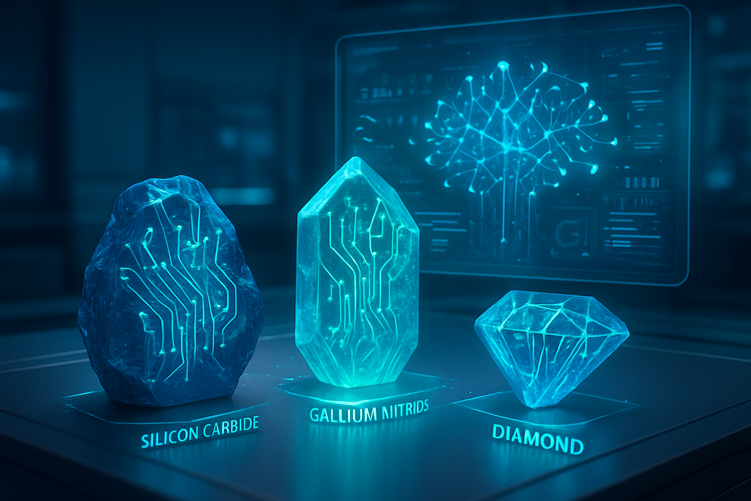
  • ON Semiconductor Navigates Shifting Sands: Q4 2025 Forecast Signals Strategic Rebalancing Amidst Market Dynamics

    ON Semiconductor Navigates Shifting Sands: Q4 2025 Forecast Signals Strategic Rebalancing Amidst Market Dynamics

    ON Semiconductor (NASDAQ: ON) has unveiled its financial outlook for the fourth quarter of 2025, projecting revenues between $1.48 billion and $1.58 billion. This guidance, released on November 3, 2025, alongside its third-quarter results, offers a crucial glimpse into the company's anticipated performance and strategic direction in a rapidly evolving semiconductor landscape. The forecast, which largely aligns with market consensus, suggests a period of strategic re-calibration for the power and sensing solutions provider as it focuses on high-growth segments like automotive, industrial, and AI.

    The Q4 2025 projections come at a pivotal time for the semiconductor industry, which has seen fluctuating demand and supply chain adjustments. ON Semiconductor's ability to provide guidance that encompasses analyst expectations, with an anticipated adjusted earnings per share (EPS) between $0.57 and $0.67 and an adjusted gross margin of 37% to 39%, indicates a measured approach to navigating current market conditions. This forecast is a key indicator for investors and industry observers, offering insights into how the company plans to sustain its market position and drive future growth amidst both opportunities and challenges.

    Detailed Financial Projections and Market Context

    ON Semiconductor's Q4 2025 revenue forecast of $1.48 billion to $1.58 billion is a central piece of its financial narrative. This range brackets the market's consensus estimate of $1.53 billion, suggesting a degree of confidence in the company's internal models and market understanding. Accompanying this revenue outlook, the company has guided for an adjusted EPS of $0.57 to $0.67, comfortably encompassing the analyst estimate of $0.62. Furthermore, an adjusted gross margin projection of 37% to 39% aligns closely with the market's expectation of 37.8%, underscoring a consistent operational strategy.

    To put these projections into perspective, the company's third-quarter (Q3) 2025 performance saw revenues of $1.55 billion, slightly surpassing analyst estimates of $1.52 billion. The Q3 adjusted EPS of $0.63 also exceeded the anticipated $0.59. While Q3 2025 revenue marked a 12% decrease year-over-year, it represented a 6% sequential increase compared to Q2 2025 revenue of $1.47 billion. This sequential growth indicates some recovery or stabilization in demand following earlier dips.

    However, a closer look at the year-over-year comparison reveals a more challenging picture. The Q4 2025 revenue forecast of $1.48 billion to $1.58 billion reflects a notable decline when compared to the Q4 2024 revenue of $1.72 billion. This year-over-year contraction suggests ongoing market headwinds or a strategic re-prioritization away from certain less profitable segments. The company's focus on high-value applications within automotive, industrial, and AI is a deliberate move to counteract broader market softness and improve margin profiles.

    Initial reactions from the financial community have been cautious but largely in line with expectations. Analysts are closely watching the company's ability to execute on its strategy to shift its product mix towards higher-margin, more specialized solutions, particularly in the silicon carbide (SiC) market. The current forecast indicates that while the overall revenue might see some contraction, the underlying profitability and strategic direction remain key areas of focus for ON Semiconductor.

    Market Positioning and Competitive Dynamics in a Shifting Landscape

    ON Semiconductor's Q4 2025 revenue forecast, coupled with its aggressive strategic focus on intelligent power and sensing solutions for the automotive, industrial, and AI data center markets, significantly shapes its competitive standing. The company's substantial investments in silicon carbide (SiC) and gallium nitride (GaN) technologies, alongside its emphasis on energy efficiency, are critical differentiators in a market contested by formidable rivals such as Infineon Technologies, STMicroelectronics (STM), and Wolfspeed.

    The company's commitment to SiC technology is exemplified by its $2 billion investment in a vertically integrated SiC manufacturing facility in the Czech Republic. This move aims to secure its supply chain for power semiconductors, particularly vital for electric vehicle (EV) electrification, where SiC demand is projected to grow at a robust 25% Compound Annual Growth Rate (CAGR) through 2030. This vertical integration strategy, part of its "Fab Right" initiative, not only aims to boost margins but also to reduce reliance on external suppliers, directly challenging competitors like Wolfspeed, which historically held an advantage in SiC materials.

    Against Infineon Technologies, a long-standing leader in automotive semiconductors and SiC, ON Semiconductor's robust growth in SiC and its direct focus on automotive and AI power management position it as a strong contender. Infineon's partnerships with entities like NVIDIA for AI data centers and its leading market share in SiC demonstrate the intensity of this competition. Similarly, STMicroelectronics, which commands the largest share of the SiC market at approximately 35%, finds itself in direct competition with ON Semiconductor's 25% SiC market share and its strong ADAS sensor portfolio, where ON Semiconductor holds a 60% market share. As both companies heavily invest in SiC fabrication, the battle for market dominance in this high-growth area is set to intensify.

    The broader tech industry stands to benefit from ON Semiconductor's innovations, particularly in enhanced energy efficiency. The company's vGaN and SiC technologies are crucial for the energy efficiency revolution in EVs and edge AI systems, leading to smaller, lighter, and more efficient components. This translates into optimized AI infrastructure, lower costs per rack in AI data centers, and advancements in edge AI and IoT applications. However, this strategic shift also brings potential disruptions, including increased market concentration benefiting top suppliers, potential resource allocation imbalances at foundries prioritizing AI chips, and the growing pricing power of dominant players like NVIDIA. The shift towards in-house chip design by automotive OEMs also presents a long-term challenge to traditional semiconductor supplier relationships, requiring ON Semiconductor to continuously innovate and adapt its offerings.

    Wider Significance: Powering the AI Revolution Sustainably

    ON Semiconductor's strategic pivot towards energy-efficient power and sensing solutions, particularly through its advancements in Silicon Carbide (SiC) and Gallium Nitride (GaN) technologies, is not merely a corporate strategy but a fundamental response to the most pressing challenges and opportunities in the broader AI landscape. The explosive growth of AI, from large language models to complex autonomous systems, is creating unprecedented demands on power infrastructure, making energy efficiency a paramount concern for the industry's sustainability and scalability.

    This strategic alignment addresses the critical trend of AI's escalating energy consumption. With data center electricity usage projected to more than double by 2030, ON Semiconductor's focus on reducing power losses in conversion processes using SiC and GaN is vital. These wide-bandgap semiconductors offer superior performance, enabling higher operating voltages, faster switching frequencies, and improved thermal management, which directly translates into significantly greater energy efficiency and power density. This is crucial for the "sustainable AI" movement, aiming to mitigate the environmental impact of AI's rapid expansion.

    The impacts of this strategy are far-reaching. Environmentally, by significantly reducing energy consumption in data centers and electric vehicles, these technologies contribute to mitigating climate change, easing the burden on national power grids, and accelerating the transition to renewable energy sources. Economically, lower energy consumption translates to reduced operational costs for AI data centers and industrial applications, supporting the scalable deployment of AI technologies. Technologically, SiC and GaN enable higher power density, smaller footprints, and lighter systems, allowing for more compact and powerful AI infrastructure, extended EV range, and more efficient industrial machinery. This is essential for achieving "all-day AI" on portable devices and in edge computing scenarios, where AI processing occurs closer to the data source.

    However, this rapid advancement is not without its concerns. Even with efficiency improvements, the exponential growth of AI's computational demand could still strain existing electrical grids and infrastructure. The manufacturing complexity and higher costs of SiC and GaN semiconductors compared to traditional silicon chips could hinder widespread adoption and increase lead times. Furthermore, for critical infrastructure like data centers, operators prioritize reliability, demanding continuous demonstration of the long-term robustness of these advanced solutions. The immense cooling requirements of large AI data centers also lead to significant water consumption, a growing environmental concern.

    Comparing this era to previous AI milestones reveals a distinct shift. While early AI was hardware-limited and later advancements focused on specialized processors like GPUs for deep learning, the current phase is defined by a materials-level revolution in power electronics. The focus has moved beyond just computational power to holistic system optimization, with energy efficiency becoming a primary driver. This makes the adoption of advanced materials like SiC and GaN, and the power management solutions they enable, as transformative for sustaining AI's growth as the advent of GPUs was for enabling deep learning. It underscores that the future of AI is not just about faster chips, but about smarter, more sustainable power delivery.

    Future Developments and Horizon Applications

    ON Semiconductor's strategic blueprint, underpinned by its Q4 2025 forecast and sustained investments in SiC, GaN, and intelligent sensing, positions the company for significant long-term growth despite near-term cyclical headwinds. The company's "Fab Right" approach and vertical integration strategy are designed to optimize manufacturing and secure supply chains, targeting an impressive 10% to 12% Compound Annual Growth Rate (CAGR) from 2022 through 2027, significantly outpacing the overall semiconductor market.

    In the near term, the company anticipates a recovery in demand during the second half of 2025, particularly in its core automotive and industrial markets, following a period of inventory reduction and moderation in EV sales. However, the long-term outlook is far more robust, driven by the relentless expansion of electric vehicles, renewable energy, and artificial intelligence. ON Semiconductor is actively developing new 4th generation trench-based SiC MOSFETs, aiming to transition to 8-inch SiC wafer platforms by 2025, and expanding its SiC capacity five-fold by 2026. This aggressive stance is intended to capture 35-40% of the SiC market, which is projected to reach $10 billion by 2030.

    The re-entry and significant investment in the GaN market, highlighted by the acquisition of NexGen Power Systems' fabrication facility, signal a strong commitment to this next-generation power technology. The company's groundbreaking vertical GaN (vGaN) power semiconductors promise to reduce energy losses by nearly 50% and enable significantly smaller, lighter systems, poised for high-demand applications in AI data centers (800V DC-DC converters), electric vehicles (more efficient inverters for increased range), and faster charging infrastructure. Experts predict the GaN market will expand at a CAGR exceeding 25% through the late 2020s.

    On the intelligent sensing front, ON Semiconductor plans to launch a new family of image sensors in 2025 and has bolstered its portfolio with the acquisition of SWIR Vision Systems. These advancements are crucial for enhancing Advanced Driver Assistance Systems (ADAS) and machine vision, extending visibility beyond standard CMOS sensors, and supporting applications in industrial automation, medical imaging, and aerospace/defense. The company's strong market share in automotive ADAS image sensors (68% in 2023) underscores its leadership and potential for continued growth in these high-value segments.

    However, challenges persist. The semiconductor industry's inherent cyclicality, intense competition in the SiC and GaN markets, and ongoing geopolitical tensions affecting global supply chains remain significant hurdles. The high cost and complexity of manufacturing advanced SiC and GaN chips, along with the need to consistently demonstrate their long-term reliability, are critical for broader market adoption. Despite these challenges, expert predictions generally maintain an optimistic long-term view. Analysts forecast a sharp rebound in earnings and revenue for ON Semiconductor in 2026, with earnings per share expected to increase by 36.8% year-over-year. The "AI supercycle" is widely expected to drive above-average growth for the semiconductor industry, pushing the global market beyond $1 trillion by 2030, with ON Semiconductor well-positioned to capitalize on this expansion through its strategic focus on the foundational technologies powering this revolution.

    Comprehensive Wrap-Up: Steering Towards an Electrified, AI-Powered Future

    ON Semiconductor's Q4 2025 revenue forecast and its overarching strategic direction paint a clear picture of a company meticulously navigating a complex, yet opportunity-rich, semiconductor landscape. While the projected revenue range of $1.48 billion to $1.58 billion reflects some near-term market adjustments and a year-over-year decline from Q4 2024, it also underscores a deliberate pivot towards high-growth, high-margin segments: electric vehicles (EVs), industrial automation, and artificial intelligence (AI). This strategic refinement, coupled with a robust "Fab Right" manufacturing approach and significant investments in Silicon Carbide (SiC) and Gallium Nitride (GaN) technologies, positions ON Semiconductor as a foundational enabler of future technological advancements.

    In the context of AI history, ON Semiconductor's current trajectory marks a crucial phase where hardware efficiency and power management have become as critical as computational power itself. Unlike earlier AI milestones that primarily focused on raw processing capabilities, the current "AI supercycle" demands sophisticated power solutions to address the unprecedented energy consumption of AI data centers and the low-power requirements of edge AI devices. By pioneering energy-efficient SiC and GaN solutions and advanced intelligent sensing, ON Semiconductor is not just participating in the AI revolution; it is providing the essential infrastructure to make it sustainable and scalable. This focus on "from the grid to the core" power delivery for AI systems makes the company an indispensable player in ensuring AI's continued expansion.

    The long-term impact on the semiconductor industry and the broader AI landscape will be substantial. ON Semiconductor's commitment to vertical integration in SiC, its re-entry into the GaN market with groundbreaking vGaN technology, and its enhanced intelligent sensing portfolio will drive resilience and market share gains. This strategic emphasis is expected to fuel significant margin expansion, with an ambitious target of 53% by 2027. Furthermore, its diversified manufacturing footprint offers a geopolitical advantage, mitigating risks associated with trade tensions. As AI models become more complex and pervasive, and as the world accelerates its transition to electrification, ON Semiconductor's role in providing efficient, robust, and intelligent power and sensing solutions will only grow in importance, solidifying its technological leadership.

    In the coming weeks and months, several critical indicators will be vital to watch. The pace of recovery in the automotive market, particularly EV adoption rates in key regions like China and Europe, will offer insights into near-term demand. Progress towards ON Semiconductor's ambitious 30-40% SiC market share target and the successful ramp-up of its new 4th generation SiC MOSFETs will be key performance metrics. Continued acceleration of revenue from AI data center solutions and the tangible benefits derived from recent acquisitions and partnerships will signal the success of its strategic pivot. Finally, the execution of its "Fab Right" strategy, including the impact of exiting legacy products on gross margins, will be closely scrutinized in future earnings reports. These factors will collectively determine ON Semiconductor's ability to capitalize on the profound shifts reshaping the global semiconductor and AI landscapes.


    This content is intended for informational purposes only and represents analysis of current AI developments.

    TokenRing AI delivers enterprise-grade solutions for multi-agent AI workflow orchestration, AI-powered development tools, and seamless remote collaboration platforms.
    For more information, visit https://www.tokenring.ai/.
  • Navitas Semiconductor Soars on AI Hopes: A Deep Dive into its Market Ascent and Future Prospects

    Navitas Semiconductor Soars on AI Hopes: A Deep Dive into its Market Ascent and Future Prospects

    San Jose, CA – October 21, 2025 – Navitas Semiconductor (NASDAQ: NVTS), a pure-play, next-generation power semiconductor company, has captured significant market attention throughout 2025, experiencing an extraordinary rally in its stock price. This surge is primarily fueled by burgeoning optimism surrounding its pivotal role in the artificial intelligence (AI) revolution and the broader shift towards highly efficient power solutions. While the company's all-time high was recorded in late 2021, its recent performance, particularly in the latter half of 2024 and through 2025, underscores a renewed investor confidence in its wide-bandgap (WBG) Gallium Nitride (GaN) and Silicon Carbide (SiC) technologies.

    The company's stock, which had already shown robust growth, saw an accelerated climb, soaring over 520% year-to-date by mid-October 2025 and nearly 700% from its year-to-date low in early April. As of October 19, 2025, NVTS shares were up approximately 311% year-to-date, closing around $17.10 on October 20, 2025. This remarkable performance reflects a strong belief in Navitas's ability to address critical power bottlenecks in high-growth sectors, particularly electric vehicles (EVs) and, most significantly, the rapidly expanding AI data center infrastructure. The market's enthusiasm is a testament to the perceived necessity of Navitas's innovative power solutions for the next generation of energy-intensive computing.

    The Technological Edge: Powering the Future with GaN and SiC

    Navitas Semiconductor's market position is fundamentally anchored in its pioneering work with Gallium Nitride (GaN) and Silicon Carbide (SiC) power semiconductors. These advanced materials represent a significant leap beyond traditional silicon-based power electronics, offering unparalleled advantages in efficiency, speed, and power density. Navitas's GaNFast™ and GeneSiC™ technologies integrate power, drive, control, sensing, and protection onto a single chip, effectively creating highly optimized power ICs.

    The technical superiority of GaN and SiC allows devices to operate at higher voltages and temperatures, switch up to 100 times faster, and achieve superior energy conversion efficiency. This directly translates into smaller, lighter, and more energy-efficient power systems. For instance, in fast-charging applications, Navitas's GaN solutions enable compact, high-power chargers that can rapidly replenish device batteries. In more demanding environments like data centers and electric vehicles, these characteristics are critical. The ability to handle high voltages (e.g., 800V architectures) with minimal energy loss and thermal dissipation is a game-changer for systems that consume massive amounts of power. This contrasts sharply with previous silicon-based approaches, which often required larger form factors, more complex cooling systems, and inherently suffered from greater energy losses, making them less suitable for the extreme demands of modern AI computing and high-performance EVs. Initial reactions from the AI research community and industry experts highlight GaN and SiC as indispensable for the next wave of technological innovation, particularly as power consumption becomes a primary limiting factor for AI scale.

    Reshaping the AI and EV Landscape: Who Benefits?

    Navitas Semiconductor's advancements are poised to significantly impact a wide array of AI companies, tech giants, and startups. Companies heavily invested in building and operating AI data centers stand to benefit immensely. Tech giants like NVIDIA (NASDAQ: NVDA), a recent strategic partner, will find Navitas's GaN and SiC solutions crucial for their next-generation 800V DC AI factory computing platforms. This partnership not only validates Navitas's technology but also positions it as a key enabler for the leading edge of AI infrastructure.

    The competitive implications for major AI labs and tech companies are substantial. Those who adopt advanced WBG power solutions will gain strategic advantages in terms of energy efficiency, operational costs, and the ability to scale their computing power more effectively. This could disrupt existing products or services that rely on less efficient power delivery, pushing them towards obsolescence. For instance, traditional power supply manufacturers might need to rapidly integrate GaN and SiC into their offerings to remain competitive. Navitas's market positioning as a pure-play specialist in these next-generation materials gives it a significant strategic advantage, as it is solely focused on optimizing these technologies for emerging high-growth markets. Its ability to enable a 100x increase in server rack power capacity by 2030 speaks volumes about its potential to redefine data center design and operation.

    Beyond AI, the electric vehicle (EV) sector is another major beneficiary. Navitas's GaN and SiC solutions facilitate faster EV charging, greater design flexibility, and are essential for advanced 800V architectures that support bidirectional charging and help meet stringent emissions targets. Design wins, such as the GaN-based EV onboard charger with China's leading EV manufacturer Changan Auto, underscore its growing influence in this critical market.

    Wider Significance: Powering the Exascale Future

    Navitas Semiconductor's rise fits perfectly into the broader AI landscape and the overarching trend towards sustainable and highly efficient technology. As AI models grow exponentially in complexity and size, the energy required to train and run them becomes a monumental challenge. Traditional silicon power conversion is reaching its limits, making wide-bandgap semiconductors like GaN and SiC not just an improvement, but a necessity. This development highlights a critical shift in the AI industry: while focus often remains on chips and algorithms, the underlying power infrastructure is equally vital for scaling AI.

    The impacts extend beyond energy savings. Higher power density means smaller, lighter systems, reducing the physical footprint of data centers and EVs. This is crucial for environmental sustainability and resource optimization. Potential concerns, however, include the rapid pace of adoption and the ability of the supply chain to keep up with demand for these specialized materials. Comparisons to previous AI milestones, such as the development of powerful GPUs, show that enabling technologies for underlying infrastructure are just as transformative as the computational engines themselves. Navitas’s role is akin to providing the high-octane fuel and efficient engine management system for the AI supercars of tomorrow.

    The Road Ahead: What to Expect

    Looking ahead, Navitas Semiconductor is poised for significant near-term and long-term developments. The partnership with Powerchip Semiconductor Manufacturing Corp (PSMC) for 200mm GaN-on-Si wafer production, with initial output expected in the first half of 2026, aims to expand manufacturing capacity, lower costs, and support its ambitious roadmap for AI data centers. The company also reported over 430 design wins in 2024, representing a potential associated revenue of $450 million, indicating a strong pipeline for future growth, though the conversion of these wins into revenue can take 2-4 years for complex projects.

    Potential applications and use cases on the horizon include further penetration into industrial power, solar energy, and home appliances, leveraging the efficiency benefits of GaN and SiC. Experts predict that Navitas will continue to introduce advanced power platforms, with 4.5kW GaN/SiC platforms pushing power densities and 8-10kW platforms planned by late 2024 to meet 2025 AI power requirements. Challenges that need to be addressed include Navitas's current unprofitability, as evidenced by revenue declines in Q1 and Q2 2025, and periods of anticipated market softness in sectors like solar and EV in the first half of 2025. Furthermore, its high valuation (around 61 times expected sales) places significant pressure on future growth to justify current prices.

    A Crucial Enabler in the AI Era

    In summary, Navitas Semiconductor's recent stock performance and the surrounding market optimism are fundamentally driven by its strategic positioning at the forefront of wide-bandband semiconductor technology. Its GaN and SiC solutions are critical enablers for the next generation of high-efficiency power conversion, particularly for the burgeoning demands of AI data centers and the rapidly expanding electric vehicle market. The strategic partnership with NVIDIA is a key takeaway, solidifying Navitas's role in the most advanced AI computing platforms.

    This development marks a significant point in AI history, underscoring that infrastructure and power efficiency are as vital as raw computational power for scaling artificial intelligence. The long-term impact of Navitas's technology could be profound, influencing everything from the environmental footprint of data centers to the range and charging speed of electric vehicles. What to watch for in the coming weeks and months includes the successful ramp-up of its PSMC manufacturing partnership, the conversion of its extensive design wins into tangible revenue, and the company's progress towards sustained profitability. The market will closely scrutinize how Navitas navigates its high valuation amidst continued investment in scaling its innovative power solutions.


    This content is intended for informational purposes only and represents analysis of current AI developments.

    TokenRing AI delivers enterprise-grade solutions for multi-agent AI workflow orchestration, AI-powered development tools, and seamless remote collaboration platforms.
    For more information, visit https://www.tokenring.ai/.