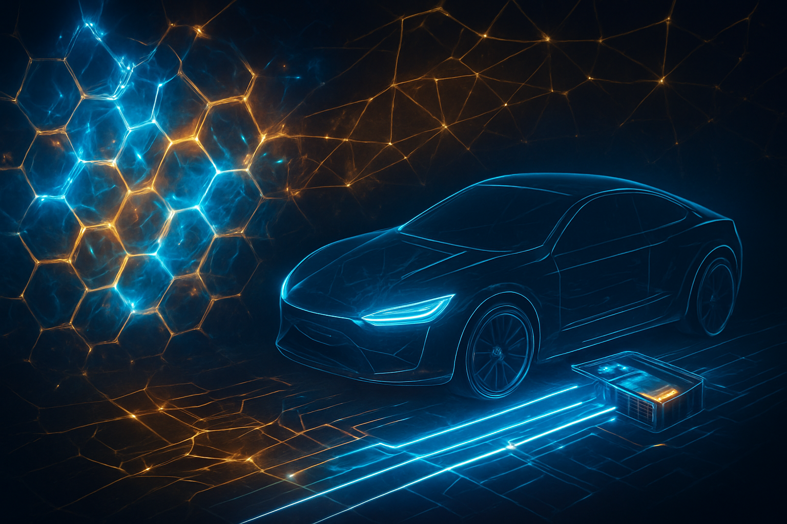
As of January 23, 2026, the automotive industry has reached a pivotal tipping point in its electrification journey, driven by the explosive rise of wide-bandgap (WBG) materials. Silicon Carbide (SiC) and Gallium Nitride (GaN) have transitioned from high-end specialized components to the essential backbone of modern power electronics. This shift is not just a hardware upgrade; it is being accelerated by sophisticated artificial intelligence systems that are optimizing material discovery, manufacturing yields, and real-time power management. The global Silicon Carbide market is now firmly on a trajectory to surpass $10 billion by the end of the decade, as it systematically dismantles the long-standing dominance of traditional silicon-based semiconductors.
The immediate significance of this development lies in the democratization of the 800V electric vehicle (EV) architecture. While 800V systems were previously reserved for luxury performance vehicles, the integration of SiC and GaN, paired with AI-driven design tools, has brought ultra-fast charging and extended range to mass-market models. For consumers, this means the era of the "15-minute charge" has finally arrived. For the tech industry, it represents the merging of advanced material science with AI-orchestrated manufacturing, creating a more resilient and efficient energy ecosystem.
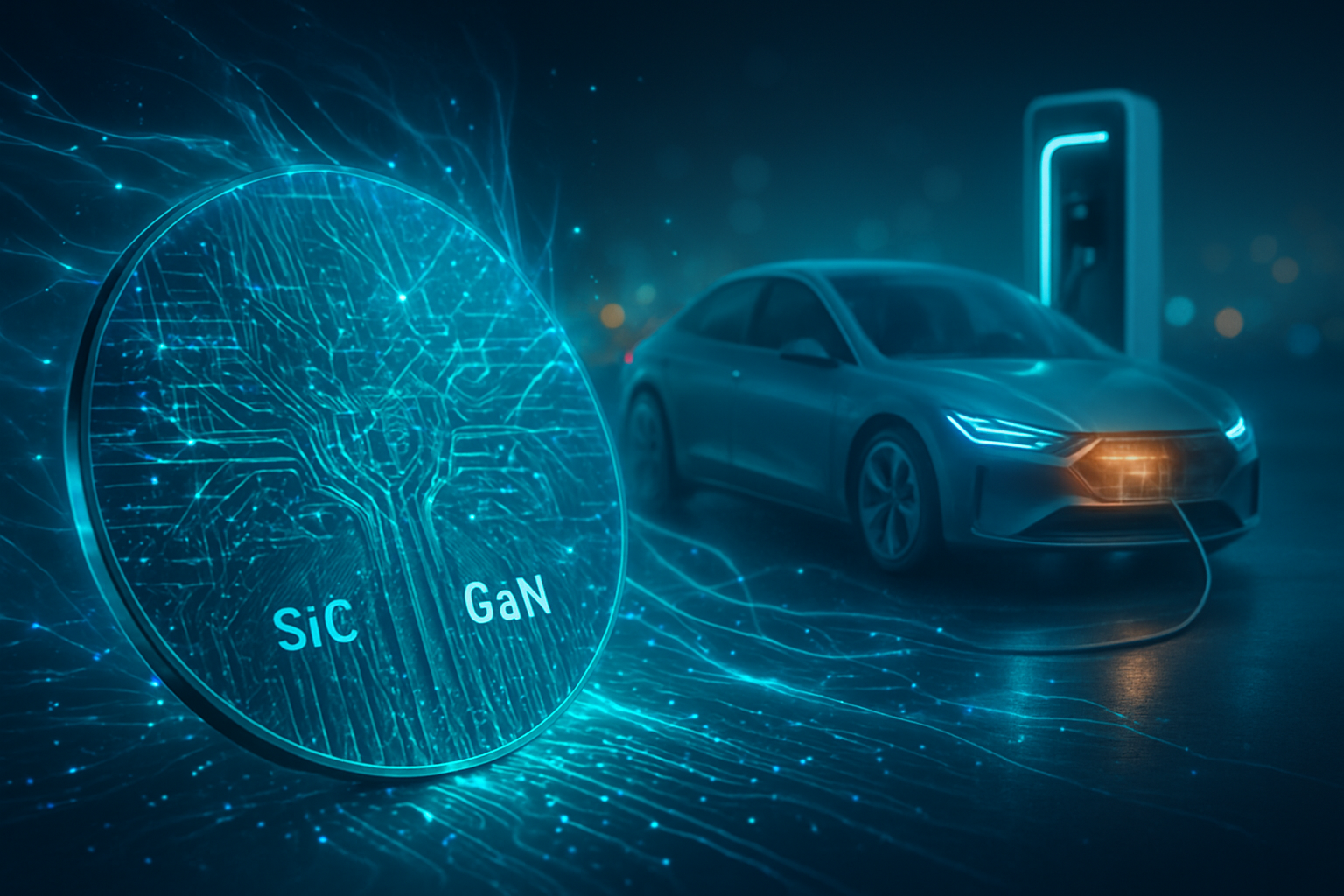
Engineering the 800V Standard: The WBG Technical Edge
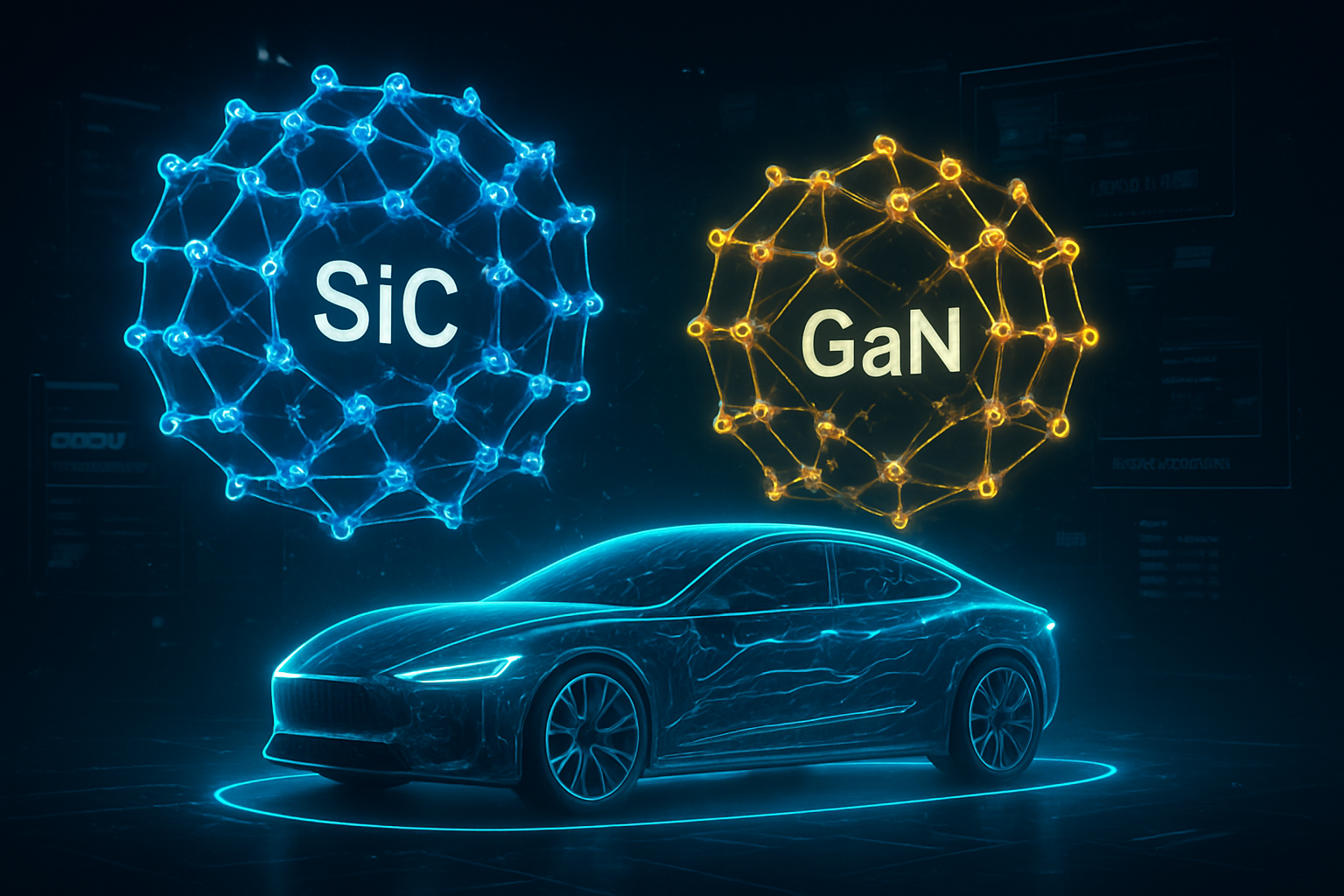
The transition from traditional Silicon (Si) Insulated Gate Bipolar Transistors (IGBTs) to Silicon Carbide and Gallium Nitride represents one of the most significant leaps in power electronics history. Unlike traditional silicon, SiC and GaN possess a much wider "bandgap"—the energy range where no electron states can exist. This physical property allows these materials to operate at much higher voltages, temperatures, and frequencies. Specifically, SiC’s thermal conductivity is roughly 3.5 times higher than silicon’s, enabling it to dissipate heat far more effectively and operate at temperatures exceeding 200°C.
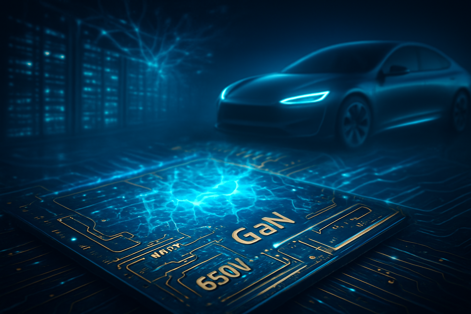
These technical specifications have profound implications for EV design. By moving to an 800V architecture enabled by SiC, automakers can double the voltage and halve the current required for the same power output. This allows for the use of thinner, lighter copper wiring—reducing vehicle weight by upwards of 30 pounds—and slashes internal resistance losses. Efficiency in power conversion has jumped from roughly 94% with silicon to over 99% with SiC and GaN. Furthermore, the high switching speeds of GaN (which can exceed 1 MHz) allow for significantly smaller inductors and capacitors, shrinking the overall size of on-board chargers and DC-DC converters by up to 50%.
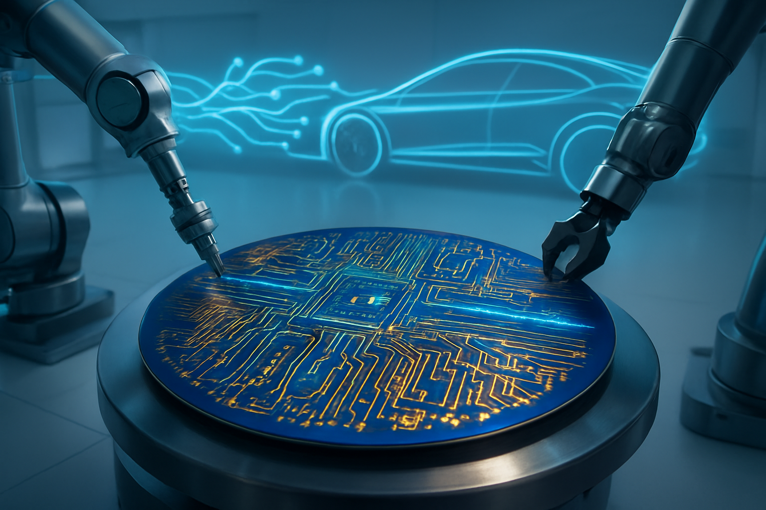
Initial reactions from the semiconductor research community have highlighted that the "yield wall" of WBG materials is finally being scaled. Historically, SiC was difficult to manufacture due to its extreme hardness and the complexity of growing defect-free crystals. However, the introduction of AI-driven predictive modeling in late 2024 and throughout 2025 has revolutionized the growth process. Industry experts at the 2026 Applied Power Electronics Conference (APEC) noted that AI-enhanced defect detection has boosted 200mm (8-inch) wafer yields by nearly 20%, making these materials economically viable for the first time for budget-tier vehicles.
The Corporate Battlefield: Leaders in the $10B SiC Market
The shift toward WBG materials has reorganized the competitive landscape for major semiconductor players. STMicroelectronics (NYSE: STM), currently the market leader in SiC device supply, has solidified its position through a massive integrated "SiC Campus" in Italy. By utilizing AI for real-time performance analytics across its global sites, STM has maintained a dominant share of the supply chain for leading EV manufacturers. Meanwhile, Wolfspeed (NYSE: WOLF) has emerged from its 2025 financial restructuring as a leaner, 200mm-focused powerhouse, leveraging AI-driven "Material Informatics" to discover new substrate compositions that improve reliability and lower costs.
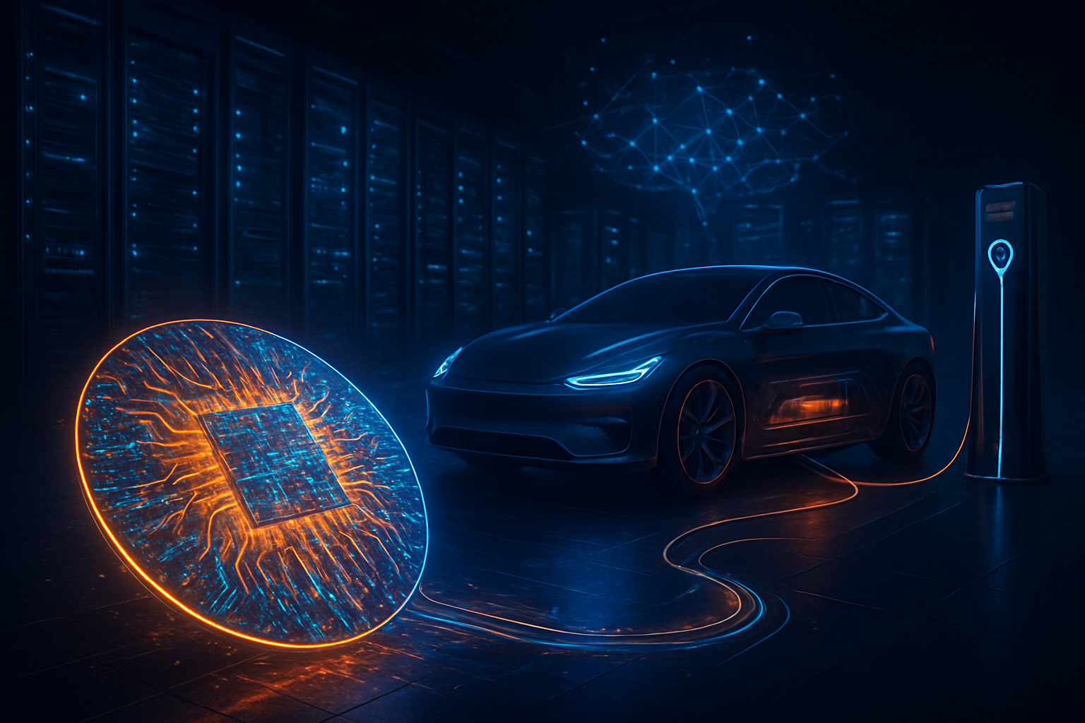
Other tech giants are rapidly positioning themselves to capture the burgeoning market. ON Semiconductor (NASDAQ: ON), also known as Onsemi, has focused on high-density packaging, using AI-simulated thermal models to cram more power into smaller modules. Infineon Technologies (OTC: IFNNY) has successfully launched its CoolSiC Gen2 line, which has become the standard for high-performance OEMs. Even Tesla (NASDAQ: TSLA), which famously announced a 75% reduction in SiC content per vehicle in 2023, has actually deepened the industry's sophistication; they are using custom AI Electronic Design Automation (EDA) tools to perform "chip-to-system co-design," allowing them to extract more performance from fewer, more power-dense SiC chips.
This development is significantly disrupting existing products. Traditional silicon IGBT manufacturers are seeing their automotive order books evaporate as OEMs switch to WBG for all new platforms. Startups in the "GaN-on-Silicon" space are also benefiting, as they offer a lower-cost entry point for 400V systems and auxiliary power modules, putting pressure on legacy providers to pivot or face obsolescence. The market positioning now favors those who can integrate AI at the manufacturing level to ensure the highest possible reliability.
Broader Significance: AI Integration and the Sustainability Mandate
The rise of WBG materials is inextricably linked to the broader AI landscape. We are seeing a "double-ended" AI benefit: AI is used to design and build these chips, and these chips are, in turn, powering the high-voltage infrastructure needed for AI data centers. "Material Informatics"—the application of AI to material science—has cut the time needed for device modeling and Process Design Kit (PDK) development from years to months. This allows for rapid iteration of new chip architectures that can handle the massive energy demands of modern technological society.
From a sustainability perspective, the impact is immense. Increasing EV efficiency by just 5% through SiC adoption is equivalent to removing millions of tons of CO2 from the atmosphere over the lifecycle of a global fleet. However, the transition is not without concerns. The manufacturing of SiC is significantly more energy-intensive than traditional silicon, leading some to question the "green-ness" of the production phase. Furthermore, the concentration of SiC substrate production in a handful of high-tech facilities has raised supply chain security concerns similar to those seen during the 2021 chip shortage.
Comparatively, the shift to SiC is being viewed by historians as the "Silicon-to-Gallium" moment for the 21st century—reminiscent of the transition from vacuum tubes to transistors. It represents a fundamental change in the physics of our power systems, moving away from "managing heat" to "eliminating losses."
The Road Ahead: AI on the Chip and Mass Adoption
Looking toward 2027 and beyond, the next frontier is "AI on the chip." We are seeing the first generation of AI-driven gate drivers—chips that include embedded machine learning kernels to monitor the thermal health of a transistor in real-time. These smart drivers can predict a component failure before it happens and adjust switching patterns to mitigate damage or optimize efficiency on the fly. This predictive maintenance will be vital for the rollout of autonomous Robotaxis, where vehicle uptime is the most critical metric.
Experts predict that as the SiC market crosses the $10 billion threshold, we will see a surge in "GaN-on-SiC" and even Diamond-based semiconductors for niche aerospace and extreme-environment applications. The near-term challenge remains the scale-up of 200mm wafer production. While yield rates are improving, the industry must continue to invest in automated, AI-controlled foundries to meet the projected demand of 30 million EVs per year by 2030.
Summary and Outlook
The transition to wide-bandgap materials like SiC and GaN, accelerated by AI, marks a definitive end to the "Silicon Age" for automotive power electronics. Key takeaways include the standardization of the 800V architecture, the use of AI to solve complex manufacturing hurdles, and the emergence of a multi-billion-dollar market led by players like STM, Wolfspeed, and Infineon.
In the history of AI and technology, this development will be remembered as the moment when "Material Informatics" proved its value, turning a difficult-to-handle crystal into the engine of the global energy transition. In the coming weeks and months, watch for major announcements from mass-market automakers regarding 800V platform standardizations and further breakthroughs in AI-integrated power management systems. The power revolution is no longer coming; it is already here.
This content is intended for informational purposes only and represents analysis of current AI developments.
TokenRing AI delivers enterprise-grade solutions for multi-agent AI workflow orchestration, AI-powered development tools, and seamless remote collaboration platforms.
For more information, visit https://www.tokenring.ai/.