Phoenix, AZ – November 18, 2025 – ON Semiconductor (NASDAQ: ON), a leading provider of intelligent power and sensing technologies, today announced a new and expansive $6 billion share repurchase program. This significant financial maneuver, set to commence on January 1, 2026, and run for three years through December 31, 2028, effectively doubles the company's previous $3 billion authorization. The announcement, made concurrently with the current date, signals a strong vote of confidence from management in the company's financial health, long-term strategic direction, and a belief that its shares are currently undervalued.
The immediate significance of this colossal buyback is multi-faceted. It represents a substantial commitment of capital, amounting to approximately one-third of the company's current market capitalization of $18.34 billion. Thad Trent, ON Semiconductor's Executive Vice President and CFO, underscored that doubling the authorization demonstrates a dedication to disciplined capital management and creating long-term shareholder value. This move also highlights the company's robust liquidity, with a current ratio of 5.23, and a history of aggressive share repurchases, having utilized nearly 100% of its free cash flow in 2025 for buybacks under the expiring program.
Financial Power Play: Unpacking the $6 Billion Share Repurchase
The $6 billion share repurchase program is a clear signal of ON Semiconductor's financial strength and its strategic approach to capital allocation. The program offers flexibility, allowing repurchases through various methods, including open market purchases, privately negotiated transactions, or Rule 10b5-1 trading plans, with timing dependent on market conditions and stock prices. This flexibility allows the company to opportunistically acquire shares.
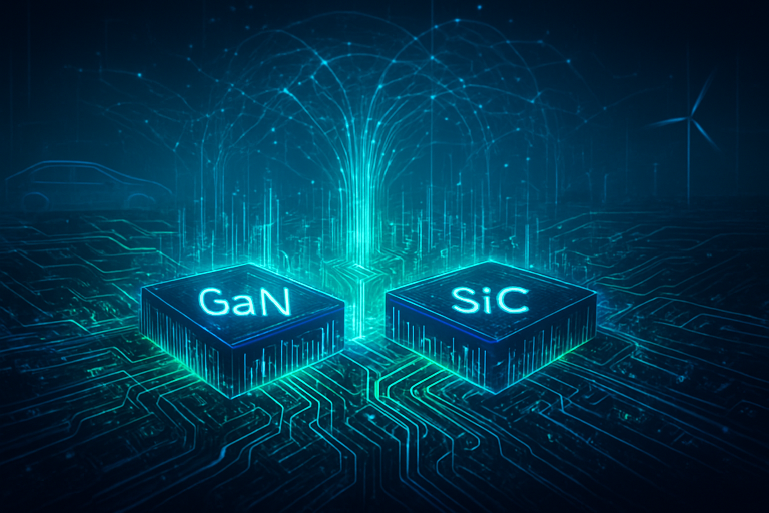
This new authorization significantly expands upon a prior $3 billion program that is set to expire on December 31, 2025. Under the previous program, ON Semiconductor had already repurchased $2.1 billion of its common stock over the preceding three years, including a notable allocation of approximately 100% of its free cash flow in 2025 to share repurchases. This aggressive approach indicates a consistent strategy of returning capital to shareholders. Historically, ON Semiconductor has also focused on transforming its business by divesting from legacy, low-growth segments and investing heavily in higher-growth, higher-margin industries like automotive and industrial, particularly in advanced power solutions such as Silicon Carbide (SiC) and Gallium Nitride (GaN). This "Fab Right" strategy aims to optimize manufacturing for higher-value products and expand gross margins.
The financial implications of such a large buyback are substantial. Primarily, it is expected to boost Earnings Per Share (EPS) by reducing the number of outstanding shares. Assuming constant or growing net income, fewer shares mean a larger slice of earnings for each remaining share. This can make the stock more attractive to investors and potentially lead to a higher stock valuation. Management's decision to repurchase shares often signals their belief that the stock is undervalued, projecting confidence in future earnings and the company's prospects. This is particularly relevant given that ON Semiconductor shares were trading down approximately 27% year-to-date and appeared undervalued by some estimates prior to the announcement. On the balance sheet, the buyback will reduce cash holdings and total assets, simultaneously decreasing shareholders' equity. However, this can also improve metrics like Return on Equity (ROE), making the company appear more efficient. Crucially, ON Semiconductor's strong liquidity and moderate debt levels suggest it can fund this buyback without undue financial strain.
Market Responds Positively as Investors Eye Long-Term Value
The market's reaction to ON Semiconductor's (NASDAQ: ON) $6 billion share buyback announcement was immediately positive. Following the news, ON Semiconductor's shares experienced an uplift, trading higher in extended hours. This positive movement came as the stock had been trading lower year-to-date, suggesting that the buyback could serve as a significant catalyst for a rebound, especially given independent assessments of the company's undervaluation.
Financial analysts largely viewed the substantial share repurchase program favorably. A Capital Allocation Analyst expressed a positive outlook, noting the doubling of the buyback authorization. Analysts generally interpret such significant buybacks as a strong signal of management's confidence in the company's future performance and cash flow visibility. This confidence, combined with the EPS boost from a reduced share count, is seen as supportive of the stock's valuation. InvestingPro highlighted ON Semiconductor's aggressive share buyback strategy as a key characteristic of its management. While some analysts, like Piper Sandler, had recently adjusted price targets due to broader industry multiples, the overall sentiment around the buyback itself was positive, affirming a commitment to shareholder value.
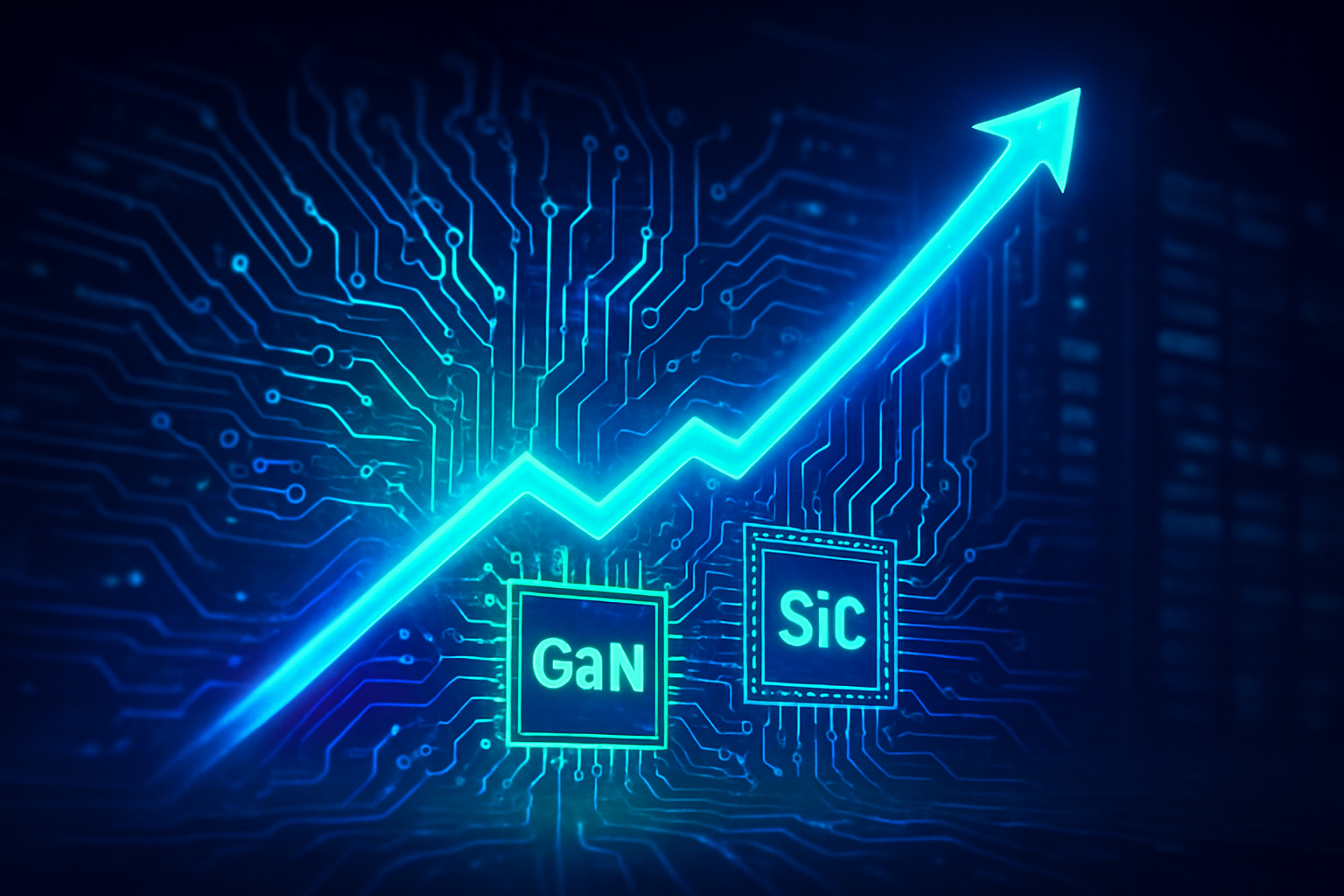
For current investors, the $6 billion share buyback signifies a strong dedication to returning capital, potentially leading to increased EPS and a higher stock valuation. It reinforces management's belief in the company's intrinsic value and future prospects, serving as a positive indicator of long-term value creation and financial stability. Prospective investors might view the buyback as an opportune moment, suggesting that management considers the stock undervalued. The commitment to consistent capital returns, coupled with ON Semiconductor's strategic focus on high-growth sectors like automotive, industrial automation, and AI data centers through investments in SiC and GaN technologies, could make it an attractive option for those seeking companies with disciplined financial management and exposure to future market trends. However, prospective investors should also weigh the potential impact of significant capital allocation to buybacks on the scale of future direct investments in R&D or other growth initiatives.
Strategic Reinforcement: Aligning Buybacks with Growth Ambitions
ON Semiconductor's (NASDAQ: ON) $6 billion share repurchase program is not merely a financial transaction; it's a strategic maneuver that reinforces the company's long-term vision and disciplined approach to growth. The program, commencing in 2026, underscores management's unwavering confidence in its financial health, consistent cash flow generation, and its strategic pivot towards high-growth, high-margin markets.
The buyback aligns directly with ON Semiconductor's stated long-term goals of creating shareholder value and maintaining disciplined capital allocation. CEO Hassane El-Khoury emphasized that the increased program reflects confidence in the company's strategic direction. This capital management strategy is supported by ambitious financial targets, including a goal of achieving a 53% non-GAAP gross margin by 2027 and a revenue compound annual growth rate (CAGR) of 10-12% from 2022 to 2027, outpacing the broader semiconductor market. Furthermore, ON Semiconductor aims to convert approximately 25% of its revenue into free cash flow by 2025.
Crucially, the share buyback program does not signal a retreat from strategic investments in critical technologies. ON Semiconductor remains committed to advancing its differentiated power and sensing technologies, particularly in Silicon Carbide (SiC) and Gallium Nitride (GaN). These advanced materials are foundational for next-generation power solutions and are central to the company's growth strategy in electric vehicles (EVs), sustainable energy grids, industrial automation, and AI data centers. The company is actively ramping up its SiC production to support long-term supply agreements and aims to capture 40% market share in the SiC segment by 2027 through strategic brownfield investments. While navigating recent headwinds in the EV market, the long-term outlook for SiC demand remains robust. The buyback demonstrates management's confidence in its cash generation capabilities even while making significant capital expenditures to scale SiC capacity.
ON Semiconductor is strategically focused on high-growth megatrends. Its pivotal role in providing analog and power solutions for vehicle electrification, industrial automation, and AI data centers is solidified through partnerships, such as with Volkswagen Group, utilizing ON Semiconductor's EliteSiC technology in electric vehicles. The company's emphasis on onshore production also provides a competitive advantage and a "derisked" partnership for global automakers. Any perceived "shifts" in strategic focus are more accurately described as strategic optimizations. The company is undergoing restructuring and cost reduction initiatives through non-cash impairment and accelerated depreciation charges as part of its "Fab Right" strategy. This aims to optimize its manufacturing footprint for greater efficiency and improved return on invested capital, prioritizing high-growth areas rather than redirecting its strategic path.
Broader Implications: A Semiconductor Industry Trend
ON Semiconductor's (NASDAQ: ON) $6 billion share buyback program is a significant event that resonates within the broader semiconductor industry landscape, reflecting current trends in corporate finance and capital allocation. This substantial capital return program, representing a sizable portion of the company's market capitalization, signals a clear commitment to shareholder value and management's confidence in its future cash flow generation.
The buyback fits into an industry landscape characterized by cyclical shifts and increasing capital allocation to emerging technologies. After a challenging 2023, the semiconductor market is poised for a rebound in 2024 and significant growth in 2025, driven by megatrends like artificial intelligence (AI), electric vehicles (EVs), and industrial automation—areas where ON Semiconductor is strategically positioned. While global semiconductor capital expenditure saw a dip, a rebound is anticipated, particularly for AI chips. However, share buybacks have become a prevalent feature across the tech sector, with a sharp uptick expected in 2024 and 2025, fueled by strong cash generation and, in some cases, investor pressure for direct returns.
A common concern raised with large buyback programs is their potential impact on critical long-term investments, such as Research and Development (R&D) and capital expenditures. Critics argue that such programs can divert resources from innovation. However, ON Semiconductor's management has explicitly emphasized its continued investment in "differentiated technologies across power and sensing that will define the next generation of intelligent, energy-efficient systems." The company's focus on ramping silicon carbide capacity and its "Fab Right" restructuring efforts suggest a strategy of optimizing operations and investing in high-growth areas while simultaneously returning capital to shareholders. Some research even suggests that share repurchases can promote R&D expenditure rather than reduce it in the high-tech industry. The challenge for companies like ON Semiconductor is to strike a balance between rewarding shareholders and ensuring sufficient investment for long-term competitiveness.
ON Semiconductor's buyback is not an isolated incident. Many major players in the semiconductor industry have engaged in similar or even larger capital return programs. Intel (NASDAQ: INTC), for instance, spent over $30 billion on buybacks from 2019 to 2023, even while receiving substantial CHIPS Act subsidies for manufacturing expansion. Advanced Micro Devices (NASDAQ: AMD) recently announced a $6 billion buyback, adding to an existing authorization, bringing its total to $10 billion. Analog Devices (NASDAQ: ADI) also spent $9 billion on buybacks between 2019 and 2023. This trend reflects a broader industry shift where strong financial positions are being used for both direct shareholder remuneration and strategic growth initiatives, often in response to strong cash flows and investor demands.
Future Horizons: Sustained Growth and Emerging Challenges
Following the substantial $6 billion share buyback authorization, ON Semiconductor (NASDAQ: ON) is strategically positioned for significant future developments, capitalizing on its strengths in intelligent power and sensing technologies. The buyback program, while a strong commitment to shareholder value, is complementary to the company's aggressive pursuit of growth in critical market segments.
In the near term, ON Semiconductor is navigating a mixed market landscape. While facing a current slowdown in the Electric Vehicle (EV) market due to elevated interest rates and inventory adjustments, a recovery is anticipated. The company is actively monitoring demand and has secured key design wins in China's EV ecosystem, with product ramps expected in the second half of 2025. The industrial segment, which experienced an earlier decline, is expected to rebound sooner, with ON Semiconductor planning to broaden its analog/mixed-signal product lineup and introduce new image sensors in 2025. Furthermore, the company is undergoing restructuring and cost-reduction initiatives as part of its "Fab Right" strategy, aiming to reduce costs by 30% by 2026. Management expects the second quarter of 2025 to mark the bottom for the automotive market, with overall signs of recovery emerging.
Long-term developments for ON Semiconductor are centered on capitalizing on several megatrends. Continued emphasis on automotive electrification and safety will drive demand for SiC technology to improve battery efficiency, extend range, and enable smaller, lighter power conversion systems. The global EV market is projected to reach 30% of passenger vehicle sales by 2030. The company will also see ongoing investment and expansion in industrial automation, robotics, machine vision, smart cities/buildings, and sustainable energy grids. Significant growth is anticipated in AI data centers and cloud infrastructure, driven by demand for intelligent power and sensing solutions, with the company's Hyperlux ID sensors and vertical GaN technology being key enablers. Strategic partnerships, such as with Nvidia (NASDAQ: NVDA), are expected to further enhance ON Semiconductor's capabilities in AI and industrial applications. Management aims to convert approximately 25% of its revenue into free cash flow by 2025 and forecasts revenue growth of 10-12% CAGR from 2022 through 2027, targeting a gross margin of 53% by 2027.
Potential applications and use cases on the horizon span across its core markets: in automotive, this includes EVs, Advanced Driver-Assistance Systems (ADAS), autonomous driving, and EV charging stations; in industrial, it encompasses industrial automation, robotics, sustainable energy grids, and medical imaging; and in AI/Cloud, it involves AI data centers, cloud infrastructure power management, and 5G infrastructure.
Despite the optimistic outlook, ON Semiconductor faces several challenges. High exposure to the automotive sector makes it vulnerable to cyclical downturns and EV adoption rate fluctuations. The industry is also currently dealing with excess inventory, impacting near-term revenue. Intense competition, particularly in the SiC market, and broader geopolitical and supply chain risks also pose challenges. Furthermore, execution risks associated with ramping SiC production and the "Fab Right" transition could impact margin targets.
Experts generally maintain a positive outlook, predicting a strong recovery for ON Semiconductor, with expected earnings growth of 29% by 2026 as the automotive market stabilizes and AI-related demand increases. Many analyses suggest the stock is currently undervalued, presenting an attractive entry point. Some foresee ON Semiconductor positioned for a semiconductor "supercycle" driven by increasing AI adoption, with long-term forecasts projecting substantial stock price increases, reflecting confidence in the company's alignment with irreversible megatrends like electrification and automation.
Comprehensive Wrap-Up: A Confident Stride into the Future
ON Semiconductor's (NASDAQ: ON) announcement of a new $6 billion share repurchase program marks a pivotal moment in the company's financial and strategic trajectory. This aggressive move, doubling its previous authorization and commencing in January 2026, underscores a robust commitment to returning capital to shareholders and signals profound confidence in its financial resilience and long-term strategic vision.
Key takeaways from this development include the substantial capital commitment, a continuation of ON Semiconductor's aggressive share repurchase strategy, and a clear demonstration of management's belief in the company's intrinsic value. The program's flexible execution methods allow for opportunistic share acquisitions, further emphasizing a disciplined approach to capital management.
In the context of corporate finance, this buyback signifies a strategic prioritization of capital returns, aiming to enhance shareholder value through increased EPS and potentially a stronger stock valuation. Within the semiconductor industry, it highlights ON Semiconductor's unique position in high-growth, high-margin areas like automotive, industrial, and AI data centers, particularly with its differentiated Silicon Carbide (SiC) and Gallium Nitride (GaN) technologies. This move reflects a balanced strategy of investing in innovation while simultaneously rewarding shareholders, aligning with a broader industry trend where strong cash-generating companies are increasingly utilizing buybacks.
The long-term impact is expected to be positive for shareholders, potentially leading to sustained stock price appreciation and reinforcing ON Semiconductor's image as a company dedicated to both disciplined capital management and strategic growth. This dual focus is crucial for strengthening its competitive position in the rapidly evolving power and sensing technology landscape.
What to watch for in the coming weeks and months includes the actual pace and magnitude of the buyback execution, the company's ability to maintain strong free cash flow, and the performance of its strategic initiatives in core growth markets. Investors should also closely monitor quarterly financial results and guidance for insights into revenue growth, margin trends, and the anticipated 2026 rebound. The impact of recently disclosed asset impairments on near-term earnings and the broader semiconductor market conditions will also be crucial indicators for ON Semiconductor's continued success.
This content is intended for informational purposes only and represents analysis of current AI developments.
TokenRing AI delivers enterprise-grade solutions for multi-agent AI workflow orchestration, AI-powered development tools, and seamless remote collaboration platforms.
For more information, visit https://www.tokenring.ai/.