Tag: GaN

  • Navitas Semiconductor Ignites the AI Revolution with Gallium Nitride Power

    Navitas Semiconductor Ignites the AI Revolution with Gallium Nitride Power

    In a pivotal shift for the semiconductor industry, Navitas Semiconductor (NASDAQ: NVTS) is leading the charge with its groundbreaking Gallium Nitride (GaN) technology, revolutionizing power electronics and laying a critical foundation for the exponential growth of Artificial Intelligence (AI) and other advanced tech sectors. By enabling unprecedented levels of efficiency, power density, and miniaturization, Navitas's GaN solutions are not merely incremental improvements but fundamental enablers for the next generation of computing, from colossal AI data centers to ubiquitous edge AI devices. This technological leap promises to reshape how power is delivered, consumed, and managed across the digital landscape, directly addressing some of AI's most pressing challenges.

    The GaNFast™ Advantage: Powering AI's Demands with Unrivaled Efficiency

    Navitas Semiconductor's leadership stems from its innovative approach to GaN integrated circuits (ICs), particularly through its proprietary GaNFast™ and GaNSense™ technologies. Unlike traditional silicon-based power devices, Navitas's GaN ICs integrate the GaN power FET with essential drive, control, sensing, and protection circuitry onto a single chip. This integration allows for switching speeds up to 100 times faster than conventional silicon, drastically reducing switching losses and enabling significantly higher switching frequencies. The result is power electronics that are not only up to three times faster in charging capabilities but also half the size and weight, while offering substantial energy savings.

    The company's fourth-generation (4G) GaN technology boasts an industry-first 20-year warranty on its GaNFast power ICs, underscoring their commitment to reliability and robustness. This level of performance and durability is crucial for demanding applications like AI data centers, where uptime and efficiency are paramount. Navitas has already demonstrated significant market traction, shipping over 100 million GaN devices by 2024 and exceeding 250 million units by May 2025. This rapid adoption is further supported by strategic manufacturing partnerships, such as with Powerchip Semiconductor Manufacturing Corporation (PSMC) for 200mm GaN-on-silicon technology, ensuring scalability to meet surging demand. These advancements represent a profound departure from the limitations of silicon, offering a pathway to overcome the power and thermal bottlenecks that have historically constrained high-performance computing.

    Reshaping the Competitive Landscape for AI and Tech Giants

    The implications of Navitas's GaN leadership extend deeply into the competitive dynamics of AI companies, tech giants, and burgeoning startups. Companies at the forefront of AI development, particularly those designing and deploying advanced AI chips like GPUs, TPUs, and NPUs, stand to benefit immensely. The immense computational power demanded by modern AI models translates directly into escalating energy consumption and thermal management challenges in data centers. GaN's superior efficiency and power density are critical for providing the stable, high-current power delivery required by these power-hungry processors, enabling AI accelerators to operate at peak performance without succumbing to thermal throttling or excessive energy waste.

    This development creates competitive advantages for major AI labs and tech companies that can swiftly integrate GaN-based power solutions into their infrastructure. By facilitating the transition to higher voltage systems (e.g., 800V DC) within data centers, GaN can significantly increase server rack power capacity and overall computing density, a crucial factor for building the multi-megawatt "AI factories" of the future. Navitas's solutions, capable of tripling power density and cutting energy losses by 30% in AI data centers, offer a strategic lever for companies looking to optimize their operational costs and environmental footprint. Furthermore, in the electric vehicle (EV) market, companies are leveraging GaN for more efficient on-board chargers and inverters, while consumer electronics brands are adopting it for faster, smaller, and lighter chargers, all contributing to a broader ecosystem where power efficiency is a key differentiator.

    GaN's Broader Significance: A Cornerstone for Sustainable AI

    Navitas's GaN technology is not just an incremental improvement; it's a foundational enabler shaping the broader AI landscape and addressing some of the most critical trends of our time. The energy consumption of AI data centers is projected to more than double by 2030, posing significant environmental challenges. GaN semiconductors inherently reduce energy waste, minimize heat generation, and decrease the material footprint of power systems, directly contributing to global "Net-Zero" goals and fostering a more sustainable future for AI. Navitas estimates that each GaN power IC shipped reduces CO2 emissions by over 4 kg compared to legacy silicon devices, offering a tangible pathway to mitigate AI's growing carbon footprint.

    Beyond sustainability, GaN's ability to create smaller, lighter, and cooler power systems is a game-changer for miniaturization and portability. This is particularly vital for edge AI, robotics, and mobile AI platforms, where minimal power consumption and compact size are critical. Applications range from autonomous vehicles and drones to medical robots and mobile surveillance, enabling longer operation times, improved responsiveness, and new deployment possibilities in remote or constrained environments. This widespread adoption of GaN represents a significant milestone, comparable to previous breakthroughs in semiconductor technology that unlocked new eras of computing, by providing the robust, efficient power infrastructure necessary for AI to truly permeate every aspect of technology and society.

    The Horizon: Expanding Applications and Addressing Future Challenges

    Looking ahead, the trajectory for Navitas's GaN technology points towards continued expansion and deeper integration across various sectors. In the near term, we can expect to see further penetration into high-power AI data centers, with more widespread adoption of 800V DC architectures becoming standard. The electric vehicle market will also continue to be a significant growth area, with GaN enabling more efficient and compact power solutions for charging infrastructure and powertrain components. Consumer electronics will see increasingly smaller and more powerful fast chargers, further enhancing user experience.

    Longer term, the potential applications for GaN are vast, including advanced AI accelerators that demand even higher power densities, ubiquitous edge AI deployments in smart cities and IoT devices, and sophisticated power management systems for renewable energy grids. Experts predict that the superior characteristics of GaN, and other wide bandgap materials like Silicon Carbide (SiC), will continue to displace silicon in high-power, high-frequency applications. However, challenges remain, including further cost reduction to accelerate mass-market adoption in certain segments, continued scaling of manufacturing capabilities, and the need for ongoing research into even higher levels of integration and performance. As AI models grow in complexity and demand, the innovation in power electronics driven by companies like Navitas will be paramount.

    A New Era of Power for AI

    Navitas Semiconductor's leadership in Gallium Nitride technology marks a profound turning point in the evolution of power electronics, with immediate and far-reaching implications for the artificial intelligence industry. The ability of GaNFast™ ICs to deliver unparalleled efficiency, power density, and miniaturization directly addresses the escalating energy demands and thermal challenges inherent in advanced AI computing. Navitas (NASDAQ: NVTS), through its innovative GaN solutions, is not just optimizing existing systems but is actively enabling new architectures and applications, from the "AI factories" that power the cloud to the portable intelligence at the edge.

    This development is more than a technical achievement; it's a foundational shift that promises to make AI more powerful, more sustainable, and more pervasive. By significantly reducing energy waste and carbon emissions, GaN technology aligns perfectly with global environmental goals, making the rapid expansion of AI a more responsible endeavor. As we move forward, the integration of GaN into every facet of power delivery will be a critical factor to watch. The coming weeks and months will likely bring further announcements of new products, expanded partnerships, and increased market penetration, solidifying GaN's role as an indispensable component in the ongoing AI revolution.


    This content is intended for informational purposes only and represents analysis of current AI developments.

    TokenRing AI delivers enterprise-grade solutions for multi-agent AI workflow orchestration, AI-powered development tools, and seamless remote collaboration platforms.
    For more information, visit https://www.tokenring.ai/.

  • Ga-Polar LEDs Illuminate the Future: A Leap Towards Brighter Displays and Energy-Efficient AI

    Ga-Polar LEDs Illuminate the Future: A Leap Towards Brighter Displays and Energy-Efficient AI

    The landscape of optoelectronics is undergoing a transformative shift, driven by groundbreaking advancements in Gallium-polar (Ga-polar) Light-Emitting Diodes (LEDs). These innovations, particularly in the realm of micro-LED technology, promise not only to dramatically enhance light output and efficiency but also to lay critical groundwork for the next generation of displays, augmented reality (AR), virtual reality (VR), and even energy-efficient artificial intelligence (AI) hardware. Emerging from intensive research primarily throughout 2024 and 2025, these developments signal a pivotal moment in the ongoing quest for superior light sources and more sustainable computing.

    These breakthroughs are directly tackling long-standing challenges in LED technology, such as the persistent "efficiency droop" at high current densities and the complexities of achieving monolithic full-color displays. By optimizing carrier injection, manipulating polarization fields, and pioneering novel device architectures, researchers and companies are unlocking unprecedented performance from GaN-based LEDs. The immediate significance lies in the potential for substantially more efficient and brighter devices, capable of powering everything from ultra-high-definition screens to the optical interconnects of future AI data centers, setting a new benchmark for optoelectronic performance.

    Unpacking the Technical Marvels: A Deeper Dive into Ga-Polar LED Innovations

    The recent surge in Ga-polar LED advancements stems from a multi-pronged approach to overcome inherent material limitations and push the boundaries of quantum efficiency and light extraction. These technical breakthroughs represent a significant departure from previous approaches, addressing fundamental issues that have historically hampered LED performance.

    One notable innovation is the n-i-p GaN barrier, introduced for the final quantum well in GaN-based LEDs. This novel design creates a powerful reverse electrostatic field that significantly enhances electron confinement and improves hole injection efficiency, leading to a remarkable 105% boost in light output power at 100 A/cm² compared to conventional LEDs. This direct manipulation of carrier dynamics within the active region is a sophisticated approach to maximize radiative recombination.

    Further addressing the notorious "efficiency droop," researchers at Nagoya University have made strides in low polarization GaN/InGaN LEDs. By understanding and manipulating polarization effects in the gallium nitride/indium gallium nitride (GaN/InGaN) layer structure, they achieved greater efficiency at higher power levels, particularly in the challenging green spectrum. This differs from traditional c-plane GaN LEDs which suffer from the Quantum-Confined Stark Effect (QCSE) due to strong polarization fields, separating electron and hole wave functions. The adoption of non-polar or semi-polar growth orientations or graded indium compositions directly counters this effect.

    For next-generation displays, n-side graded quantum wells for green micro-LEDs offer a significant leap. This structure, featuring a gradually varying indium content on the n-side of the quantum well, reduces lattice mismatch and defect density. Experimental results show a 10.4% increase in peak external quantum efficiency and a 12.7% enhancement in light output power at 100 A/cm², alongside improved color saturation. This is a crucial improvement over abrupt, square quantum wells, which can lead to higher defect densities and reduced electron-hole overlap.

    In terms of light extraction, the Composite Reflective Micro Structure (CRS) for flip-chip LEDs (FCLEDs) has proven highly effective. Comprising multiple reflective layers like Ag/SiO₂/distributed Bragg reflector/SiO₂, the CRS increased the light output power of FCLEDs by 6.3% and external quantum efficiency by 6.0% at 1500 mA. This multi-layered approach vastly improves upon single metallic mirrors, redirecting more trapped light for extraction. Similarly, research has shown that a roughened p-GaN surface morphology, achieved by controlling Trimethylgallium (TMGa) flow rate during p-AlGaN epilayer growth, can significantly enhance light extraction efficiency by reducing total internal reflection.

    Perhaps one of the most transformative advancements comes from Polar Light Technologies, with their pyramidal InGaN/GaN micro-LEDs. By late 2024, they demonstrated red-emitting pyramidal micro-LEDs, completing the challenging milestone of achieving true RGB emission monolithically on a single wafer using the same material system. This bottom-up, non-etching fabrication method avoids the sidewall damage and QCSE issues inherent in conventional top-down etching, enabling superior performance, miniaturization, and easier integration for AR/VR headsets and ultra-low power screens. Initial reactions from the industry have been highly enthusiastic, recognizing these breakthroughs as critical enablers for next-generation display technologies and energy-efficient AI.

    Redefining the Tech Landscape: Implications for AI Companies and Tech Giants

    The advancements in Ga-polar LEDs, particularly the burgeoning micro-LED technology, are set to profoundly reshape the competitive landscape for AI companies, tech giants, and startups alike. These innovations are not merely incremental improvements but foundational shifts that will enable new product categories and redefine existing ones.

    Tech giants are at the forefront of this transformation. Companies like Apple (NASDAQ: AAPL), which acquired Luxvue in 2014, and Samsung Electronics (KRX: 005930) are heavily investing in micro-LEDs as the future of display technology. Apple is anticipated to integrate micro-LEDs into new devices by 2024 and mass-market AR/VR devices by 2024-2025. Samsung has already showcased large micro-LED TVs and holds a leading global market share in this nascent segment. The superior brightness (up to 10,000 nits), true blacks, wider color gamut, and faster response times of micro-LEDs offer these giants a significant performance edge, allowing them to differentiate premium devices and establish market leadership in high-end markets.

    For AI companies, the impact extends beyond just displays. Micro-LEDs are emerging as a critical component for neuromorphic computing, offering the potential to create energy-efficient optical processing units that mimic biological neural networks. This could drastically reduce the energy demands of massively parallel AI computations. Furthermore, micro-LEDs are poised to revolutionize AI infrastructure by providing long-reach, low-power, and low-cost optical communication links within data centers. This can overcome the scaling limitations of current communication technologies, unlocking radical new AI cluster designs and accelerating the commercialization of Co-Packaged Optics (CPO) between AI semiconductors.

    Startups are also finding fertile ground in this evolving ecosystem. Specialized firms are focusing on critical niche areas such as mass transfer technology, which is essential for efficiently placing millions of microscopic LEDs onto substrates. Companies like X-Celeprint, Playnitride, Mikro-Mesa, VueReal, and Lumiode are driving innovation in this space. Other startups are tackling challenges like improving the luminous efficiency of red micro-LEDs, with companies like PoroTech developing solutions to enhance quality, yield, and manufacturability for full-color micro-LED displays.

    The sectors poised to benefit most include Augmented Reality/Virtual Reality (AR/VR), where micro-LEDs offer 10 times the resolution, 100 times the contrast, and 1000 times greater luminance than OLEDs, while halving power consumption. This enables lighter designs, eliminates the "screen-door effect," and provides the high pixel density crucial for immersive experiences. Advanced Displays for large-screen TVs, digital signage, automotive applications, and high-end smartphones and smartwatches will also see significant disruption, with micro-LEDs eventually challenging the dominance of OLED and LCD technologies in premium segments. The potential for transparent micro-LEDs also opens doors for new heads-up displays and smart glass applications that can visualize AI outputs and collect data simultaneously.

    A Broader Lens: Ga-Polar LEDs in the Grand Tapestry of Technology

    The advancements in Ga-polar LEDs are not isolated technical triumphs; they represent a fundamental shift that resonates across the broader technology landscape and holds significant implications for society. These developments align perfectly with prevailing tech trends, particularly the increasing demand for energy efficiency, miniaturization, and enhanced visual experiences.

    At the heart of this wider significance is the material itself: Gallium Nitride (GaN). As a wide-bandgap semiconductor, GaN is crucial for high-performance LEDs that offer exceptional energy efficiency, converting electrical energy into light with minimal waste. This directly contributes to global sustainability goals by reducing electricity consumption and carbon footprints across lighting, displays, and increasingly, AI infrastructure. The ability to create micro-LEDs with dimensions of a micrometer or smaller is paramount for high-resolution displays and integrated photonic systems, driving the miniaturization trend across consumer electronics.

    In the context of AI, these LED advancements are laying the groundwork for a more sustainable and powerful future. The exploration of microscopic LED networks for neuromorphic computing signifies a potential paradigm shift in AI hardware, mimicking biological neural networks to achieve immense energy savings (potentially by a factor of 10,000). Furthermore, micro-LEDs are critical for optical interconnects in data centers, offering high-speed, low-power, and low-cost communication links that can overcome the scaling limitations of current electronic interconnects. This directly enables the development of more powerful and efficient AI clusters and photonic Tensor Processing Units (TPUs).

    The societal impact will be felt most acutely through enhanced user experiences. Brighter, more vibrant, and higher-resolution displays in AR/VR headsets, smartphones, and large-format screens will transform how humans interact with digital information, making experiences more immersive and intuitive. The integration of AI-powered smart lighting, enabled by efficient LEDs, can optimize environments for energy management, security, and personal well-being.

    However, challenges persist. The high cost and manufacturing complexity of micro-LEDs, particularly the mass transfer of millions of microscopic dies, remain significant hurdles. Efficiency droop at high current densities, while being addressed, still requires further research, especially for longer wavelengths (the "green gap"). Material defects, crystal quality, and effective thermal management are also ongoing areas of focus. Concerns also exist regarding the "blue light hazard" from high-intensity white LEDs, necessitating careful design and usage guidelines.

    Compared to previous AI milestones, such as the advent of personal computers, the World Wide Web, or even recent generative AI breakthroughs like ChatGPT, Ga-polar LED advancements represent a fundamental shift in the hardware foundation. While earlier milestones revolutionized software, connectivity, or processing architectures, these LED innovations provide the underlying physical substrate for more powerful, scalable, and sustainable AI models. They enable new levels of energy efficiency, miniaturization, and integration that are critical for the continued growth and societal integration of AI and immersive computing, much like how the transistor enabled the digital age.

    The Horizon Ahead: Future Developments in Ga-Polar LED Technology

    The trajectory for Ga-polar LED technology is one of continuous innovation, with both near-term refinements and long-term transformative goals on the horizon. Experts predict a future where LEDs not only dominate traditional lighting but also unlock entirely new categories of applications.

    In the near term, expect continued refinement of device structures and epitaxy. This includes the widespread adoption of advanced junction-type n-i-p GaN barriers and optimized electron blocking layers to further boost internal quantum efficiency (IQE) and light extraction efficiency (LEE). Efforts to mitigate efficiency droop will persist, with research into new crystal orientations for InGaN layers showing promise. The commercialization and scaling of pyramidal micro-LEDs, which offer significantly higher efficiency for AR systems by avoiding etching damage and optimizing light emission, will also be a key focus.

    Looking to the long term, GaN-on-GaN technology is heralded as the next major leap in LED manufacturing. By growing GaN layers on native GaN substrates, manufacturers can achieve lower defect densities, superior thermal conductivity, and significantly reduced efficiency droop at high current densities. Beyond LEDs, laser lighting, based on GaN laser diodes, is identified as the subsequent major opportunity in illumination, offering highly directional output and superior lumens per watt. Further out, nanowire and quantum dot LEDs are expected to offer even higher energy efficiency and superior light quality, with nanowire LEDs potentially becoming commercially available within five years. The ultimate goal remains the seamless, cost-effective mass production of monolithic RGB micro-LEDs on a single wafer for advanced micro-displays.

    The potential applications and use cases on the horizon are vast. Beyond general illumination, micro-LEDs will redefine advanced displays for mobile devices, large-screen TVs, and crucially, AR/VR headsets and wearable projectors. In the automotive sector, GaN-based LEDs will expand beyond headlamps to transparent and stretchable displays within vehicles. Ultraviolet (UV) LEDs, particularly UVC variants, will become indispensable for sterilization, disinfection, and water purification. Furthermore, Ga-polar LEDs are central to the future of communication, enabling high-speed Visible Light Communication (LiFi) and advanced laser communication systems. Integrated with AI, these will form smart lighting systems that adapt to environments and user preferences, enhancing energy management and user experience.

    However, significant challenges still need to be addressed. The high cost of GaN substrates for GaN-on-GaN technology remains a barrier. Overcoming efficiency droop at high currents, particularly for green emission, continues to be a critical research area. Thermal management for high-power devices, low light extraction efficiency, and issues with internal quantum efficiency (IQE) stemming from weak carrier confinement and inefficient p-type doping are ongoing hurdles. Achieving superior material quality with minimal defects and ensuring color quality and consistency across mass-produced devices are also crucial. Experts predict that LEDs will achieve near-complete market dominance (87%) by 2030, with continuous efficiency gains and a strong push towards GaN-on-GaN and laser lighting. The integration with the Internet of Things (IoT) and the broadening of applications into new sectors like electric vehicles and 5G infrastructure will drive substantial market growth.

    A New Dawn for Optoelectronics and AI: A Comprehensive Wrap-Up

    The recent advancements in Ga-polar LEDs signify a profound evolution in optoelectronic technology, with far-reaching implications that extend deep into the realm of artificial intelligence. These breakthroughs are not merely incremental improvements but represent a foundational shift that promises to redefine displays, optimize energy consumption, and fundamentally enable the next generation of AI hardware.

    Key takeaways from this period of intense innovation include the successful engineering of Ga-polar structures to overcome historical limitations like efficiency droop and carrier injection issues, often mirroring or surpassing the performance of N-polar counterparts. The development of novel pyramidal micro-LED architectures, coupled with advancements in monolithic RGB integration on a single wafer using InGaN/GaN materials, stands out as a critical achievement. This has directly addressed the challenging "green gap" and the quest for efficient red emission, paving the way for significantly more efficient and compact micro-displays. Furthermore, improvements in fabrication and bonding techniques are crucial for translating these laboratory successes into scalable, commercial products.

    The significance of these developments in AI history cannot be overstated. As AI models become increasingly complex and energy-intensive, the need for efficient underlying hardware is paramount. The shift towards LED-based photonic Tensor Processing Units (TPUs) represents a monumental step towards sustainable and scalable AI. LEDs offer a more cost-effective, easily integrable, and resource-efficient alternative to laser-based solutions, enabling faster data processing with significantly reduced energy consumption. This hardware enablement is foundational for developing AI systems capable of handling more nuanced, real-time, and massive data workloads, ensuring the continued growth and innovation of AI while mitigating its environmental footprint.

    The long-term impact will be transformative across multiple sectors. From an energy efficiency perspective, continued advancements in Ga-polar LEDs will further reduce global electricity consumption and greenhouse gas emissions, making a substantial contribution to climate change mitigation. In new display technologies, these LEDs are enabling ultra-high-resolution, high-contrast, and ultra-low-power micro-displays critical for the immersive experiences promised by AR/VR. For AI hardware enablement, the transition to LED-based photonic TPUs and the use of GaN-based materials in high-power and high-frequency electronics (like 5G infrastructure) will create a more sustainable and powerful computing backbone for the AI era.

    What to watch for in the coming weeks and months includes the continued commercialization and mass production of monolithic RGB micro-LEDs, particularly for AR/VR applications, as companies like Polar Light Technologies push these innovations to market. Keep an eye on advancements in scalable fabrication and cold bonding techniques, which are crucial for high-volume manufacturing. Furthermore, observe any research publications or industry partnerships that demonstrate real-world performance gains and practical implementations of LED-based photonic TPUs in demanding AI workloads. Finally, continued breakthroughs in optimizing Ga-polar structures to achieve high-efficiency green emission will be a strong indicator of the technology's overall progress.

    The ongoing evolution of Ga-polar LED technology is more than just a lighting upgrade; it is a foundational pillar for a future defined by ubiquitous, immersive, and highly intelligent digital experiences, all powered by more efficient and sustainable technological ecosystems.


    This content is intended for informational purposes only and represents analysis of current AI developments.

    TokenRing AI delivers enterprise-grade solutions for multi-agent AI workflow orchestration, AI-powered development tools, and seamless remote collaboration platforms.
    For more information, visit https://www.tokenring.ai/.

  • Navitas Semiconductor (NVTS) Ignites AI Power Revolution with Strategic Pivot to High-Voltage GaN and SiC

    Navitas Semiconductor (NVTS) Ignites AI Power Revolution with Strategic Pivot to High-Voltage GaN and SiC

    San Jose, CA – November 11, 2025 – Navitas Semiconductor (NASDAQ: NVTS), a leading innovator in gallium nitride (GaN) and silicon carbide (SiC) power semiconductors, has embarked on a bold strategic pivot, dubbed "Navitas 2.0," refocusing its efforts squarely on the burgeoning high-power artificial intelligence (AI) markets. This significant reorientation comes on the heels of the company's Q3 2025 financial results, reported on November 3rd, 2025, which saw a considerable stock plunge following disappointing revenue and earnings per share. Despite the immediate market reaction, the company's decisive move towards AI data centers, performance computing, and energy infrastructure positions it as a critical enabler for the next generation of AI, promising a potential long-term recovery and significant impact on the industry.

    The "Navitas 2.0" strategy signals a deliberate shift away from lower-margin consumer and mobile segments, particularly in China, towards higher-growth, higher-profit opportunities where its advanced GaN and SiC technologies can provide a distinct competitive advantage. This pivot is a direct response to the escalating power demands of modern AI workloads, which are rapidly outstripping the capabilities of traditional silicon-based power solutions. By concentrating on high-power AI, Navitas aims to capitalize on the foundational need for highly efficient, dense, and reliable power delivery systems that are essential for the "AI factories" of the future.

    Powering the Future of AI: Navitas's GaN and SiC Technical Edge

    Navitas Semiconductor's strategic pivot is underpinned by its proprietary wide bandgap (WBG) gallium nitride (GaN) and silicon carbide (SiC) technologies. These materials offer a profound leap in performance over traditional silicon in high-power applications, making them indispensable for the stringent requirements of AI data centers, from grid-level power conversion down to the Graphics Processing Unit (GPU).

    Navitas's GaN solutions, including its GaNFast™ power ICs, are optimized for high-frequency, high-density DC-DC conversion. These integrated power ICs combine GaN power, drive, control, sensing, and protection, enabling unprecedented power density and energy savings. For instance, Navitas has demonstrated a 4.5 kW, 97%-efficient power supply for AI server racks, achieving a power density of 137 W/in³, significantly surpassing comparable solutions. Their 12 kW GaN and SiC platform boasts an impressive 97.8% peak efficiency. The ability of GaN devices to switch at much higher frequencies allows for smaller, lighter, and more cost-effective passive components, crucial for compact AI infrastructure. Furthermore, the advanced GaNSafe™ ICs integrate critical protection features like short-circuit protection with 350 ns latency and 2 kV ESD protection, ensuring reliability in mission-critical AI environments. Navitas's 100V GaN FET portfolio is specifically tailored for the lower-voltage DC-DC stages on GPU power boards, where thermal management and ultra-high density are paramount.

    Complementing GaN, Navitas's SiC technologies, under the GeneSiC™ brand, are designed for high-power, high-voltage, and high-reliability applications, particularly in AC grid-to-800 VDC conversion. SiC-based components can withstand higher electric fields, operate at higher voltages and temperatures, and exhibit lower conduction losses, leading to superior efficiency in power conversion. Their Gen-3 Fast SiC MOSFETs, utilizing "trench-assisted planar" technology, are engineered for world-leading performance. Navitas often integrates both GaN and SiC within the same power supply unit, with SiC handling the higher voltage totem-pole Power Factor Correction (PFC) stage and GaN managing the high-frequency LLC stage for optimal performance.

    A cornerstone of Navitas's technical strategy is its partnership with NVIDIA (NASDAQ: NVDA), a testament to the efficacy of its WBG solutions. Navitas is supplying advanced GaN and SiC power semiconductors for NVIDIA's next-generation 800V High Voltage Direct Current (HVDC) architecture, central to NVIDIA's "AI factory" computing platforms like "Kyber" rack-scale systems and future GPU solutions. This collaboration is crucial for enabling greater power density, efficiency, reliability, and scalability for the multi-megawatt rack densities demanded by modern AI data centers. Unlike traditional silicon-based approaches that struggle with rising switching losses and limited power density, Navitas's GaN and SiC solutions cut power losses by 50% or more, enabling a fundamental architectural shift to 800V DC systems that reduce copper usage by up to 45% and simplify power distribution.

    Reshaping the AI Power Landscape: Industry Implications

    Navitas Semiconductor's (NASDAQ: NVTS) strategic pivot to high-power AI markets is poised to significantly reshape the competitive landscape for AI companies, tech giants, and startups alike. The escalating power demands of AI processors necessitate a fundamental shift in power delivery, creating both opportunities and challenges across the industry.

    NVIDIA (NASDAQ: NVDA) stands as an immediate and significant beneficiary of Navitas's strategic shift. As a direct partner, NVIDIA relies on Navitas's GaN and SiC solutions to enable its next-generation 800V DC architecture for its AI factory computing. This partnership is critical for NVIDIA to overcome power delivery bottlenecks, allowing for the deployment of increasingly powerful AI processors and maintaining its leadership in the AI hardware space. Other major AI chip developers, such as Intel (NASDAQ: INTC), AMD (NASDAQ: AMD), and Google (NASDAQ: GOOGL), will likely face similar power delivery challenges and will need to adopt comparable high-efficiency, high-density power solutions to remain competitive, potentially seeking partnerships with Navitas or its rivals.

    Established power semiconductor manufacturers, including Texas Instruments (NASDAQ: TXN), Infineon (OTC: IFNNY), Wolfspeed (NYSE: WOLF), and ON Semiconductor (NASDAQ: ON), are direct competitors in the high-power GaN/SiC market. Navitas's early mover advantage in AI-specific power solutions and its high-profile partnership with NVIDIA will exert pressure on these players to accelerate their own GaN and SiC developments for AI applications. While these companies have robust offerings, Navitas's integrated solutions and focused roadmap for AI could allow it to capture significant market share. For emerging GaN/SiC startups, Navitas's strong market traction and alliances will intensify competition, requiring them to find niche applications or specialized offerings to differentiate themselves.

    The most significant disruption lies in the obsolescence of traditional silicon-based power supply units (PSUs) for advanced AI applications. The performance and efficiency requirements of next-generation AI data centers are exceeding silicon's capabilities. Navitas's solutions, offering superior power density and efficiency, could render legacy silicon-based power supplies uncompetitive, driving a fundamental architectural transformation in data centers. This shift to 800V HVDC reduces energy losses by up to 5% and copper requirements by up to 45%, compelling data centers to adapt their designs, cooling systems, and overall infrastructure. This disruption will also spur the creation of new product categories in power distribution units (PDUs) and uninterruptible power supplies (UPS) optimized for GaN/SiC technology and higher voltages. Navitas's strategic advantages include its technology leadership, early-mover status in AI-specific power, critical partnerships, and a clear product roadmap for increasing power platforms up to 12kW and beyond.

    The Broader Canvas: AI's Energy Footprint and Sustainable Innovation

    Navitas Semiconductor's (NASDAQ: NVTS) strategic pivot to high-power AI is more than just a corporate restructuring; it's a critical response to one of the most pressing challenges in the broader AI landscape: the escalating energy consumption of artificial intelligence. This shift directly addresses the urgent need for more efficient power delivery as AI's power demands are rapidly becoming a significant bottleneck for further advancement and a major concern for global sustainability.

    The proliferation of advanced AI models, particularly large language models and generative AI, requires immense computational power, translating into unprecedented electricity consumption. Projections indicate that AI's energy demand could account for 27-50% of total data center energy consumption by 2030, a dramatic increase from current levels. High-performance AI processors now consume hundreds of watts each, with future generations expected to exceed 1000W, pushing server rack power requirements from a few kilowatts to over 100 kW. Navitas's focus on high-power, high-density, and highly efficient GaN and SiC solutions is therefore not merely an improvement but an enabler for managing this exponential growth without proportionate increases in physical footprint and operational costs. Their 4.5kW platforms, combining GaN and SiC, achieve power densities over 130W/in³ and efficiencies over 97%, demonstrating a path to sustainable AI scaling.

    The environmental impact of this pivot is substantial. The increasing energy consumption of AI poses significant sustainability challenges, with data centers projected to more than double their electricity demand by 2030. Navitas's wide-bandgap semiconductors inherently reduce energy waste, minimize heat generation, and decrease the overall material footprint of power systems. Navitas estimates that each GaN power IC shipped reduces CO2 emissions by over 4 kg compared to legacy silicon chips, and SiC MOSFETs save over 25 kg of CO2. The company projects that widespread adoption of GaN and SiC could lead to a reduction of approximately 6 Gtons of CO2 per year by 2050, equivalent to the CO2 generated by over 650 coal-fired power stations. These efficiencies are crucial for achieving global net-zero carbon ambitions and translate into lower operational costs for data centers, making sustainable practices economically viable.

    However, this strategic shift is not without its concerns. The transition away from established mobile and consumer markets is expected to cause short-term revenue depression for Navitas, introducing execution risks as the company realigns resources and accelerates product roadmaps. Analysts have raised questions about sustainable cash burn and the intense competitive landscape. Broader concerns include the potential strain on existing electricity grids due to the "always-on" nature of AI operations and potential manufacturing capacity constraints for GaN, especially with concentrated production in Taiwan. Geopolitical factors affecting the semiconductor supply chain also pose risks.

    In comparison to previous AI milestones, Navitas's contribution is a hardware-centric breakthrough in power delivery, distinct from, yet equally vital as, advancements in processing power or data storage. Historically, computing milestones focused on miniaturization and increasing transistor density (Moore's Law) to boost computational speed. While these led to significant performance gains, power efficiency often lagged. The development of specialized accelerators like GPUs dramatically improved the efficiency of AI workloads, but the "power problem" persisted. Navitas's innovation addresses this fundamental power infrastructure, enabling the architectural changes (like 800V DC systems) necessary to support the "AI revolution." Without such power delivery breakthroughs, the energy footprint of AI could become economically and environmentally unsustainable, limiting its potential. This pivot ensures that the processing power of AI can be effectively and sustainably delivered, unlocking the full potential of future AI breakthroughs.

    The Road Ahead: Future Developments and Expert Outlook

    Navitas Semiconductor's (NASDAQ: NVTS) strategic pivot to high-power AI marks a critical juncture, setting the stage for significant near-term and long-term developments not only for the company but for the entire AI industry. The "Navitas 2.0" transformation is a bold bet on the future, driven by the insatiable power demands of next-generation AI.

    In the near term, Navitas is intensely focused on accelerating its AI power roadmap. This includes deepening its collaboration with NVIDIA (NASDAQ: NVDA), providing advanced GaN and SiC power semiconductors for NVIDIA's 800V DC architecture in AI factory computing. The company has already made substantial progress, releasing the world's first 8.5 kW AI data center power supply unit (PSU) with 98% efficiency and a 12 kW PSU for hyperscale AI data centers achieving 97.8% peak efficiency, both leveraging GaN and SiC and complying with Open Compute Project (OCP) and Open Rack v3 (ORv3) specifications. Further product introductions include a portfolio of 100V and 650V discrete GaNFast™ FETs, GaNSafe™ ICs with integrated protection, and high-voltage SiC products. The upcoming release of 650V bidirectional GaN switches and the continued refinement of digital control techniques like IntelliWeave™ promise even greater efficiency and reliability. Navitas anticipates that Q4 2025 will represent a revenue bottom, with sequential growth expected to resume in 2026 as its strategic shift gains traction.

    Looking further ahead, Navitas's long-term vision is to solidify its leadership in high-power markets, delivering enhanced business scale and quality. This involves continually advancing its AI power roadmap, aiming for PSUs with power levels exceeding 12kW. The partnership with NVIDIA is expected to evolve, leading to more specialized GaN and SiC solutions for future AI accelerators and modular data center power architectures. With a strong balance sheet and substantial cash reserves, Navitas is well-positioned to fund the capital-intensive R&D and manufacturing required for these ambitious projects.

    The broader high-power AI market is projected for explosive growth, with the global AI data center market expected to reach nearly $934 billion by 2030, driven by the demand for smaller, faster, and more energy-efficient semiconductors. This market is undergoing a fundamental shift towards newer power architectures like 800V HVDC, essential for the multi-megawatt rack densities of "AI factories." Beyond data centers, Navitas's advanced GaN and SiC technologies are critical for performance computing, energy infrastructure (solar inverters, energy storage), industrial electrification (motor drives, robotics), and even edge AI applications, where high performance and minimal power consumption are crucial.

    Despite the promising outlook, significant challenges remain. The extreme power consumption of AI chips (700-1200W per chip) necessitates advanced cooling solutions and energy-efficient designs to prevent localized hot spots. High current densities and miniaturization also pose challenges for reliable power delivery. For Navitas specifically, the transition from mobile to high-power markets involves an extended go-to-market timeline and intense competition, requiring careful execution to overcome short-term revenue dips. Manufacturing capacity constraints for GaN, particularly with concentrated production in Taiwan, and supply chain vulnerabilities also present risks.

    Experts generally agree that Navitas is well-positioned to maintain a leading role in the GaN power device market due to its integrated solutions and diverse application portfolio. The convergence of AI, electrification, and sustainable energy is seen as the primary accelerator for GaN technology. However, investors remain cautious, demanding tangible design wins and clear pathways to near-term profitability. The period of late 2025 and early 2026 is viewed as a critical transition phase for Navitas, where the success of its strategic pivot will become more evident. Continued innovation in GaN and SiC, coupled with a focus on sustainability and addressing the unique power challenges of AI, will be key to Navitas's long-term success and its role in enabling the next era of artificial intelligence.

    Comprehensive Wrap-Up: A Pivotal Moment for AI Power

    Navitas Semiconductor's (NASDAQ: NVTS) "Navitas 2.0" strategic pivot marks a truly pivotal moment in the company's trajectory and, more broadly, in the evolution of AI infrastructure. The decision to shift from lower-margin consumer electronics to the demanding, high-growth arena of high-power AI, driven by advanced GaN and SiC technologies, is a bold, necessary, and potentially transformative move. While the immediate aftermath of its Q3 2025 results saw a stock plunge, reflecting investor apprehension about short-term financial performance, the long-term implications position Navitas as a critical enabler for the future of artificial intelligence.

    The key takeaway is that the scaling of AI is now inextricably linked to advancements in power delivery. Traditional silicon-based solutions are simply insufficient for the multi-megawatt rack densities and unprecedented power demands of modern AI data centers. Navitas, with its superior GaN and SiC wide bandgap semiconductors, offers a compelling solution: higher efficiency, greater power density, and enhanced reliability. Its partnership with NVIDIA (NASDAQ: NVDA) for 800V DC "AI factory" architectures is a strong validation of its technological leadership and strategic foresight. This shift is not just about incremental improvements; it's about enabling a fundamental architectural transformation in how AI is powered, reducing energy waste, and fostering sustainability.

    In the grand narrative of AI history, this development aligns with previous hardware breakthroughs that unlocked new computational capabilities. Just as specialized processors like GPUs accelerated AI training, advancements in efficient power delivery are now crucial to sustain and scale these powerful systems. Without companies like Navitas addressing the "power problem," the energy footprint of AI could become economically and environmentally unsustainable, limiting its potential. This pivot signifies a recognition that the physical infrastructure underpinning AI is as critical as the algorithms and processing units themselves.

    In the coming weeks and months, all eyes will be on Navitas's execution of its "Navitas 2.0" strategy. Investors and industry observers will be watching for tangible design wins, further product deployments in AI data centers, and clear signs of revenue growth in its new target markets. The pace at which Navitas can transition its business, manage competitive pressures from established players, and navigate potential supply chain challenges will determine the ultimate success of this ambitious repositioning. If successful, Navitas Semiconductor could emerge not just as a survivor of its post-Q3 downturn, but as a foundational pillar in the sustainable development and expansion of the global AI ecosystem.


    This content is intended for informational purposes only and represents analysis of current AI developments.

    TokenRing AI delivers enterprise-grade solutions for multi-agent AI workflow orchestration, AI-powered development tools, and seamless remote collaboration platforms.
    For more information, visit https://www.tokenring.ai/.

  • America’s Power Play: GaN Chips and the Resurgence of US Manufacturing

    America’s Power Play: GaN Chips and the Resurgence of US Manufacturing

    The United States is experiencing a pivotal moment in its technological landscape, marked by a significant and accelerating trend towards domestic manufacturing of power chips. This strategic pivot, heavily influenced by government initiatives and substantial private investment, is particularly focused on advanced materials like Gallium Nitride (GaN). As of late 2025, this movement holds profound implications for national security, economic leadership, and the resilience of critical supply chains, directly addressing vulnerabilities exposed by recent global disruptions.

    At the forefront of this domestic resurgence is GlobalFoundries (NASDAQ: GFS), a leading US-based contract semiconductor manufacturer. Through strategic investments, facility expansions, and key technology licensing agreements—most notably a recent partnership with Taiwan Semiconductor Manufacturing Company (NYSE: TSM) for GaN technology—GlobalFoundries is cementing its role in bringing cutting-edge power chip production back to American soil. This concerted effort is not merely about manufacturing; it's about securing the foundational components for the next generation of artificial intelligence, electric vehicles, and advanced defense systems, ensuring that the US remains a global leader in critical technological innovation.

    GaN Technology: Fueling the Next Generation of Power Electronics

    The shift towards GaN power chips represents a fundamental technological leap from traditional silicon-based semiconductors. As silicon CMOS technologies approach their physical and performance limits, GaN emerges as a superior alternative, offering a host of advantages that are critical for high-performance and energy-efficient applications. Its inherent material properties allow GaN devices to operate at significantly higher voltages, frequencies, and temperatures with vastly reduced energy loss compared to their silicon counterparts.

    Technically, GaN's wide bandgap and high electron mobility enable faster switching speeds and lower on-resistance, translating directly into greater energy efficiency and reduced heat generation. This superior performance allows for the design of smaller, lighter, and more compact electronic components, a crucial factor in space-constrained applications ranging from consumer electronics to electric vehicle powertrains and aerospace systems. This departure from previous silicon-centric approaches is not merely an incremental improvement but a foundational change, promising increased power density and overall system miniaturization. The semiconductor industry, including leading research institutions and industry experts, has reacted with widespread enthusiasm, recognizing GaN as a critical enabler for future technological advancements, particularly in power management and RF applications.

    GlobalFoundries' recent strategic moves underscore the importance of GaN. On November 10, 2025, GlobalFoundries announced a significant technology licensing agreement with TSMC for 650V and 80V GaN technology. This partnership is designed to accelerate GF’s development and US-based production of next-generation GaN power chips. The licensed technology will be qualified at GF's Burlington, Vermont facility, leveraging its existing expertise in high-voltage GaN-on-Silicon. Development is slated for early 2026, with production ramping up later that year, making products available by late 2026. This move positions GF to provide a robust, US-based GaN supply chain for a global customer base, distinguishing it from fabs primarily located in Asia.

    Competitive Implications and Market Positioning in the AI Era

    The growing emphasis on US-based GaN power chip manufacturing carries significant implications for a diverse range of companies, from established tech giants to burgeoning AI startups. Companies heavily invested in power-intensive technologies stand to benefit immensely from a secure, domestic supply of high-performance GaN chips. Electric vehicle manufacturers, for instance, will find more robust and efficient solutions for powertrains, on-board chargers, and inverters, potentially accelerating the development of next-generation EVs. Similarly, data center operators, constantly seeking to reduce energy consumption and improve efficiency, will leverage GaN-based power supplies to minimize operational costs and environmental impact.

    For major AI labs and tech companies, the availability of advanced GaN power chips manufactured domestically translates into enhanced supply chain security and reduced geopolitical risks, crucial for maintaining uninterrupted research and development cycles. Companies like Apple (NASDAQ: AAPL), SpaceX, AMD (NASDAQ: AMD), Qualcomm Technologies (NASDAQ: QCOM), NXP (NASDAQ: NXPI), and GM (NYSE: GM) are already committing to reshoring semiconductor production and diversifying their supply chains, directly benefiting from GlobalFoundries' expanded capabilities. This trend could disrupt existing product roadmaps that relied heavily on overseas manufacturing, potentially shifting competitive advantages towards companies with strong domestic partnerships.

    In terms of market positioning, GlobalFoundries is strategically placing itself as a critical enabler for the future of power electronics. By focusing on differentiated GaN-based power capabilities in Vermont and investing $16 billion across its New York and Vermont facilities, GF is not just expanding capacity but also accelerating growth in AI-enabling and power-efficient technologies. This provides a strategic advantage for customers seeking secure, high-performance power devices manufactured in the United States, thereby fostering a more resilient and geographically diverse semiconductor ecosystem. The ability to source critical components domestically will become an increasingly valuable differentiator in a competitive global market, offering both supply chain stability and potential intellectual property protection.

    Broader Significance: Reshaping the Global Semiconductor Landscape

    The resurgence of US-based GaN power chip manufacturing represents a critical inflection point in the broader AI and semiconductor landscape, signaling a profound shift towards greater supply chain autonomy and technological sovereignty. This initiative directly addresses the geopolitical vulnerabilities exposed by the global reliance on a concentrated few regions for advanced chip production, particularly in East Asia. The CHIPS and Science Act, with its substantial funding and strategic guardrails, is not merely an economic stimulus but a national security imperative, aiming to re-establish the United States as a dominant force in semiconductor innovation and production.

    The impacts of this trend are multifaceted. Economically, it promises to create high-skilled jobs, stimulate regional economies, and foster a robust ecosystem of research and development within the US. Technologically, the domestic production of advanced GaN chips will accelerate innovation in critical sectors such as AI, 5G/6G communications, defense systems, and renewable energy, where power efficiency and performance are paramount. This move also mitigates potential concerns around intellectual property theft and ensures a secure supply of components vital for national defense infrastructure. Comparisons to previous AI milestones reveal a similar pattern of foundational technological advancements driving subsequent waves of innovation; just as breakthroughs in processor design fueled early AI, secure and advanced power management will be crucial for scaling future AI capabilities.

    The strategic importance of this movement cannot be overstated. By diversifying its semiconductor manufacturing base, the US is building resilience against future geopolitical disruptions, natural disasters, or pandemics that could cripple global supply chains. Furthermore, the focus on GaN, a technology critical for high-performance computing and energy efficiency, positions the US to lead in the development of greener, more powerful AI systems and sustainable infrastructure. This is not just about manufacturing chips; it's about laying the groundwork for sustained technological leadership and safeguarding national interests in an increasingly interconnected and competitive world.

    Future Developments: The Road Ahead for GaN and US Manufacturing

    The trajectory for US-based GaN power chip manufacturing points towards significant near-term and long-term developments. In the immediate future, the qualification of TSMC-licensed GaN technology at GlobalFoundries' Vermont facility, with production expected to commence in late 2026, will mark a critical milestone. This will rapidly increase the availability of domestically produced, advanced GaN devices, serving a global customer base. We can anticipate further government incentives and private investments flowing into research and development, aiming to push the boundaries of GaN technology even further, exploring higher voltage capabilities, improved reliability, and integration with other advanced materials.

    On the horizon, potential applications and use cases are vast and transformative. Beyond current applications in EVs, data centers, and 5G infrastructure, GaN chips are expected to play a crucial role in next-generation aerospace and defense systems, advanced robotics, and even in novel energy harvesting and storage solutions. The increased power density and efficiency offered by GaN will enable smaller, lighter, and more powerful devices, fostering innovation across numerous industries. Experts predict a continued acceleration in the adoption of GaN, especially as manufacturing costs decrease with economies of scale and as the technology matures further.

    However, challenges remain. Scaling production to meet burgeoning demand, particularly for highly specialized GaN-on-silicon wafers, will require sustained investment in infrastructure and a skilled workforce. Research into new GaN device architectures and packaging solutions will be essential to unlock its full potential. Furthermore, ensuring that the US maintains its competitive edge in GaN innovation against global rivals will necessitate continuous R&D funding and strategic collaborations between industry, academia, and government. The coming years will see a concerted effort to overcome these hurdles, solidifying the US position in this critical technology.

    Comprehensive Wrap-up: A New Dawn for American Chipmaking

    The strategic pivot towards US-based manufacturing of advanced power chips, particularly those leveraging Gallium Nitride technology, represents a monumental shift in the global semiconductor landscape. Key takeaways include the critical role of government initiatives like the CHIPS and Science Act in catalyzing domestic investment, the superior performance and efficiency of GaN over traditional silicon, and the pivotal leadership of companies like GlobalFoundries in establishing a robust domestic supply chain. This development is not merely an economic endeavor but a national security imperative, aimed at fortifying critical infrastructure and maintaining technological sovereignty.

    This movement's significance in AI history is profound, as secure and high-performance power management is foundational for the continued advancement and scaling of artificial intelligence systems. The ability to domestically produce the energy-efficient components that power everything from data centers to autonomous vehicles will directly influence the pace and direction of AI innovation. The long-term impact will be a more resilient, geographically diverse, and technologically advanced semiconductor ecosystem, less vulnerable to external disruptions and better positioned to drive future innovation.

    In the coming weeks and months, industry watchers should closely monitor the progress at GlobalFoundries' Vermont facility, particularly the qualification and ramp-up of the newly licensed GaN technology. Further announcements regarding partnerships, government funding allocations, and advancements in GaN research will provide crucial insights into the accelerating pace of this transformation. The ongoing commitment to US-based manufacturing of power chips signals a new dawn for American chipmaking, promising a future of enhanced security, innovation, and economic leadership.


    This content is intended for informational purposes only and represents analysis of current AI developments.

    TokenRing AI delivers enterprise-grade solutions for multi-agent AI workflow orchestration, AI-powered development tools, and seamless remote collaboration platforms.
    For more information, visit https://www.tokenring.ai/.

  • GlobalFoundries and TSMC Forge Landmark GaN Alliance, Reshaping US Power Chip Manufacturing

    GlobalFoundries and TSMC Forge Landmark GaN Alliance, Reshaping US Power Chip Manufacturing

    In a pivotal development set to redefine the landscape of power semiconductor manufacturing, GlobalFoundries (NASDAQ: GFS) announced on November 10, 2025, a significant technology licensing agreement with Taiwan Semiconductor Manufacturing Company (NYSE: TSM). This strategic partnership focuses on advanced Gallium Nitride (GaN) technology, specifically 650V and 80V platforms, and is poised to dramatically accelerate GlobalFoundries' development and U.S.-based production of next-generation GaN power chips. The immediate significance lies in fortifying the domestic supply chain for critical power components, addressing burgeoning demand across high-growth sectors.

    This collaboration emerges at a crucial juncture, as TSMC, a global foundry leader, prepares to strategically exit its broader GaN foundry services by July 2027 to intensify its focus on advanced-node silicon for AI applications and advanced packaging. GlobalFoundries' acquisition of this proven GaN expertise not only ensures the continued availability and advancement of the technology but also strategically positions its Burlington, Vermont, facility as a vital hub for U.S.-manufactured GaN semiconductors, bolstering national efforts towards semiconductor independence and resilience.

    Technical Prowess: Unpacking the Advanced GaN Technology

    The licensed technology from TSMC encompasses both 650V and 80V GaN-on-Silicon (GaN-on-Si) capabilities. GlobalFoundries will leverage its existing high-voltage GaN-on-Silicon expertise at its Burlington facility to integrate and scale this technology, with a strong focus on 200mm (8-inch) wafer manufacturing for high-volume production. This move is particularly impactful as TSMC had previously developed robust second-generation GaN-on-Si processes, and GlobalFoundries is now gaining access to this established and validated technology.

    GaN technology offers substantial performance advantages over traditional silicon-based semiconductors in power applications due to its wider bandgap. Key differentiators include significantly higher energy efficiency and power density, enabling smaller, more compact designs. GaN devices boast faster switching speeds—up to 10 times faster than silicon MOSFETs and 100 times faster than IGBTs—which allows for higher operating frequencies and smaller passive components. Furthermore, GaN exhibits superior thermal performance, efficiently dissipating heat and reducing the need for complex cooling systems.

    Unlike previous approaches that relied heavily on silicon, which is reaching its performance limits in terms of efficiency and power density, GaN provides a critical leap forward. While Silicon Carbide (SiC) is another wide bandgap material, GaN-on-Silicon offers a cost-effective solution for operating voltages below 1000V by utilizing existing silicon manufacturing infrastructure. Initial reactions from the semiconductor research community and industry experts have been largely positive, viewing this as a strategic win for GlobalFoundries and a significant step towards strengthening the U.S. domestic semiconductor ecosystem, especially given TSMC's strategic pivot.

    The technology is targeted for high-performance, energy-efficient applications across various sectors, including power management solutions for data centers, industrial power applications, and critical components for electric vehicles (EVs) such as onboard chargers and DC-DC converters. It also holds promise for renewable energy systems, fast-charging electronics, IoT devices, and even aerospace and defense applications requiring robust RF and high-power control. GlobalFoundries emphasizes a holistic approach to GaN reliability, designing for harsh environments to ensure robustness and longevity.

    Market Ripple Effects: Impact on the Semiconductor Industry

    This strategic partnership carries profound implications for semiconductor companies, tech giants, and startups alike. GlobalFoundries (NASDAQ: GFS) stands as the primary beneficiary, gaining rapid access to proven GaN technology that will significantly accelerate its GaN roadmap and bolster its position as a leading contract manufacturer. This move allows GF to address the growing demand for higher efficiency and power density in power systems, offering a crucial U.S.-based manufacturing option for GaN-on-silicon semiconductors.

    For other semiconductor companies, the landscape is shifting. Companies that previously relied on TSMC (NYSE: TSM) for GaN foundry services, such as Navitas Semiconductor (NASDAQ: NVTS) and ROHM (TSE: 6963), have already begun seeking alternative manufacturing partners due to TSMC's impending exit. GlobalFoundries, with its newly acquired technology and planned U.S. production, is now poised to become a key alternative foundry, potentially capturing a significant portion of this reallocated business. This intensifies competition for established players like Infineon Technologies (OTC: IFNNY) and Innoscience, which are also major forces in the power semiconductor and GaN markets.

    Tech giants involved in cloud computing, electric vehicles, and advanced industrial equipment stand to benefit from a more diversified and robust GaN supply chain. The increased manufacturing capacity and technological expertise at GlobalFoundries will lead to a wider availability of GaN power devices, enabling these companies to integrate more energy-efficient and compact designs into their products. For startups focused on innovative GaN-based power management solutions, GlobalFoundries' entry provides a reliable manufacturing partner, potentially lowering barriers to entry and accelerating time-to-market.

    The primary disruption stems from TSMC's withdrawal from GaN foundry services, which necessitates a transition for its current GaN customers. However, GlobalFoundries' timely entry with licensed TSMC technology can mitigate some of this disruption by offering a familiar and proven process. This development significantly bolsters U.S.-based manufacturing capabilities for advanced semiconductors, enhancing market positioning and strategic advantages for GlobalFoundries by offering U.S.-based GaN capacity to a global customer base, aligning with national initiatives to strengthen domestic chip production.

    Broader Significance: A New Era for Power Electronics

    The GlobalFoundries and TSMC GaN technology licensing agreement signifies a critical juncture in the broader semiconductor manufacturing landscape, underscoring a decisive shift towards advanced materials and enhanced supply chain resilience. This partnership accelerates the adoption of GaN, a "third-generation" semiconductor material, which offers superior performance characteristics over traditional silicon, particularly in high-power and high-frequency applications. Its ability to deliver higher efficiency, faster switching speeds, and better thermal management is crucial as silicon-based CMOS technologies approach their fundamental limits.

    This move fits perfectly into current trends driven by the surging demand from next-generation technologies such as 5G telecommunications, electric vehicles, data centers, and renewable energy systems. The market for GaN semiconductor devices is projected for substantial growth, with some estimates predicting the power GaN market to reach approximately $3 billion by 2030. The agreement's emphasis on establishing U.S.-based GaN capacity directly addresses pressing concerns about supply chain resilience, especially given the geopolitical sensitivity surrounding raw materials like gallium. Diversifying manufacturing locations for critical components is a top priority for national security and economic stability.

    The impacts on global chip production are multifaceted. It promises increased availability and competition in the GaN market, offering customers an additional U.S.-based manufacturing option that could reduce lead times and geopolitical risks. This expanded capacity will enable more widespread integration of GaN into new product designs across various industries, leading to more efficient and compact electronic systems. While intellectual property (IP) is always a concern in such agreements, the history of cross-licensing and cooperation between TSMC and GlobalFoundries suggests a framework for managing such issues, allowing both companies freedom to operate and innovate.

    Comparisons to previous semiconductor industry milestones are apt. This shift from silicon to GaN for specific applications mirrors the earlier transition from germanium to silicon in the early days of transistors, driven by superior material properties. It represents a "vertical" advancement in material capability, distinct from the "horizontal" scaling achieved through lithography advancements, promising to enable new generations of power-efficient devices. This strategic collaboration also highlights the industry's evolving approach to IP, where licensing agreements facilitate technological progress rather than being bogged down by disputes.

    The Road Ahead: Future Developments and Challenges

    The GlobalFoundries and TSMC GaN partnership heralds significant near-term and long-term developments for advanced GaN power chips. In the near term, development of the licensed technology is slated to commence in early 2026 at GlobalFoundries' Burlington, Vermont facility, with initial production expected to ramp up later that year. This rapid integration aims to quickly bring high-performance GaN solutions to market, leveraging GlobalFoundries' existing expertise and significant federal funding (over $80 million since 2020) dedicated to advancing GaN-on-silicon manufacturing in the U.S.

    Long-term, the partnership is set to deliver GaN chips that will address critical power gaps across mission-critical applications in data centers, automotive, and industrial sectors. The comprehensive GaN portfolio GlobalFoundries is developing, designed for harsh environments and emphasizing reliability, will solidify GaN's role as a next-generation solution for achieving higher efficiency, power density, and compactness where traditional silicon CMOS technologies approach their limits.

    Potential applications and use cases for these advanced GaN power chips are vast and transformative. In Artificial Intelligence (AI), GaN is crucial for meeting the exponential energy demands of AI data centers, enabling power supplies to evolve for higher computational power within reduced footprints. For Electric Vehicles (EVs), GaN promises extended range and faster charging capabilities through smaller, lighter, and more efficient power conversion systems in onboard chargers and DC-DC converters, with future potential in traction inverters. In Renewable Energy, GaN will enhance energy conversion efficiency in solar inverters, wind turbine systems, and overall grid infrastructure, contributing to grid stability and decarbonization efforts.

    Despite its promising future, GaN technology faces challenges, particularly concerning U.S.-based manufacturing capabilities. These include the higher initial cost of GaN components, the complexities of manufacturing scalability and yield (such as lattice mismatch defects when growing GaN on silicon), and ensuring long-term reliability in harsh operating environments. A critical challenge for the U.S. is the current lack of sufficient domestic epitaxy capacity, a crucial step in GaN production, necessitating increased investment to secure the supply chain.

    Experts predict a rapid expansion of the GaN market, with significant growth projected through 2030 and beyond, driven by AI and electrification. GaN is expected to displace legacy silicon in many high-power applications, becoming ubiquitous in power conversion stages from consumer devices to grid-scale energy storage. Future innovations will focus on increased integration, with GaN power FETs combined with control, drive, sensing, and protection circuitry into single, high-performance GaN ICs. The transition to larger wafer sizes (300mm) and advancements in vertical GaN technology are also anticipated to further enhance efficiency and cost-effectiveness.

    A New Chapter in US Chip Independence

    The GlobalFoundries and TSMC GaN technology licensing agreement marks a monumental step, not just for the companies involved, but for the entire semiconductor industry and the broader global economy. The key takeaway is the strategic acceleration of U.S.-based GaN manufacturing, driven by a world-class technology transfer. This development is profoundly significant in the context of semiconductor manufacturing history, representing a critical shift towards advanced materials and a proactive approach to supply chain resilience.

    Its long-term impact on U.S. chip independence and technological advancement is substantial. By establishing a robust domestic hub for advanced GaN production at GlobalFoundries' Vermont facility, the U.S. gains greater control over the manufacturing of essential components for strategic sectors like defense, electric vehicles, and renewable energy. This not only enhances national security but also fosters innovation within the U.S. semiconductor ecosystem, driving economic growth and creating high-tech jobs.

    In the coming weeks and months, industry observers and consumers should closely watch for GlobalFoundries' qualification and production milestones at its Vermont facility in early 2026, followed by the availability of initial products later that year. Monitor customer adoption and design wins, particularly in the data center, industrial, and automotive sectors, as these will be crucial indicators of market acceptance. Keep an eye on the evolving GaN market pricing and competition, especially with TSMC's exit and the continued pressure from other global players. Finally, continued U.S. government support and broader technological advancements in GaN, such as larger wafer sizes and new integration techniques, will be vital to watch for as this partnership unfolds and shapes the future of power electronics.


    This content is intended for informational purposes only and represents analysis of current AI developments.

    TokenRing AI delivers enterprise-grade solutions for multi-agent AI workflow orchestration, AI-powered development tools, and seamless remote collaboration platforms.
    For more information, visit https://www.tokenring.ai/.

  • Powering Progress: Analog and Industrial Semiconductors Drive the Next Wave of Innovation

    The foundational components of our increasingly intelligent and electrified world, analog and industrial semiconductors, are undergoing a profound transformation. Far from the spotlight often cast on advanced digital processors, these critical chips are quietly enabling revolutionary advancements across electric vehicles (EVs), artificial intelligence (AI) data centers, the Industrial Internet of Things (IIoT), and renewable energy systems. Recent breakthroughs in materials science, packaging technologies, and novel computing architectures are dramatically enhancing efficiency, power density, and embedded intelligence, setting new benchmarks for performance and sustainability. This continuous wave of innovation is not merely incremental; it is fundamental to unlocking the full potential of next-generation technologies and addressing pressing global challenges like energy consumption and computational demands.

    At the forefront of this evolution, companies like ON Semiconductor (NASDAQ: ON) are driving significant advancements. Their latest offerings, including cutting-edge wide-bandgap (WBG) materials like Silicon Carbide (SiC) and Gallium Nitride (GaN), alongside sophisticated power management and sensing solutions, are crucial for managing power, converting energy, and interpreting real-world data with unprecedented precision and efficiency. The immediate significance of these developments lies in their ability to dramatically reduce energy loss, shrink device footprints, and empower intelligence closer to the data source, thereby accelerating the deployment of sustainable and smart technologies across virtually every industry.

    Technical Deep Dive: SiC, GaN, and the Rise of Analog Intelligence

    The core of the current revolution in analog and industrial semiconductors lies in the strategic shift towards wide-bandgap (WBG) materials, primarily Silicon Carbide (SiC) and Gallium Nitride (GaN). These materials possess superior electrical properties compared to traditional silicon, allowing for operation at higher temperatures, voltages, and frequencies with significantly reduced energy losses and heat generation. This inherent advantage translates directly into more efficient power conversion, faster charging capabilities for EVs, and smaller, lighter power systems across industrial applications.

    Specific details of these advancements are impressive. ON Semiconductor (NASDAQ: ON), for instance, has introduced its M3e EliteSiC MOSFETs, 1200V SiC devices that leverage planar technology to achieve industry-leading specific on-resistance while maintaining robust short-circuit capability. This pushes the boundaries of power density and efficiency, crucial for high-power applications. Similarly, their new Field Stop 7 (FS7) IGBT technology, integrated into 1200V half-bridge QDual3 IGBT modules, boasts a 33% increase in current density. This allows for the design of smaller, lighter, and more cost-effective power systems for demanding applications such as central solar inverters, energy storage, and heavy-duty commercial vehicles. Beyond power, ON Semiconductor's Hyperlux SG image sensors and Hyperlux ID family are revolutionizing indirect Time-of-Flight (iToF) depth sensing, extending accurate distance measurements and providing precise depth data on moving objects, vital for advanced robotics and autonomous systems.

    A groundbreaking development from ON Semiconductor is their vertical GaN (vGaN) power semiconductors, built on novel GaN-on-GaN technology. Unlike traditional lateral GaN devices, vGaN conducts current vertically, setting new benchmarks for power density, efficiency, and ruggedness. This innovation can reduce energy loss by almost 50% and is particularly crucial for the demanding power requirements of AI data centers, EVs, renewable energy infrastructure, and industrial automation. This vertical architecture fundamentally differs from previous lateral approaches by enabling higher operating voltages and faster switching frequencies, overcoming some of the limitations of earlier GaN implementations and offering a direct path to higher performance and greater energy savings. The initial reactions from the industry and research community highlight the transformative potential of these WBG materials and vertical architectures, recognizing them as critical enablers for the next generation of high-power and high-frequency electronics.

    The emergence of novel analog computing architectures, such as Analog Machine Learning (AnalogML), further distinguishes this wave of innovation. Companies like Aspinity are pioneering AnalogML platforms for ultra-low-power edge devices, enabling real-time data processing directly at the sensor level. This drastically reduces the need for extensive digital computation and data transfer, extending battery life and reducing latency in wearables, smart home devices, and industrial sensors. Furthermore, research into new analog processors that perform calculations directly within physical circuits, bypassing energy-intensive data transfers, is showing promise. A notable development from Peking University claims an analog AI chip capable of outperforming high-end GPUs by up to 1,000 times for certain AI tasks, while consuming significantly less energy. This "software programmable analog processor" addresses previous challenges of precision and programmability in analog systems, offering a potentially revolutionary approach to AI model training and future communication networks like 6G. These analog approaches represent a significant departure from purely digital processing, offering inherent advantages in power efficiency and speed for specific computational tasks, particularly at the edge.

    Competitive Landscape and Market Dynamics

    The ongoing advancements in analog and industrial semiconductors are reshaping the competitive landscape, creating new opportunities and challenges for tech giants, specialized AI labs, and burgeoning startups. Companies that heavily invest in and successfully deploy wide-bandgap (WBG) materials, advanced packaging, and novel analog computing solutions stand to gain significant strategic advantages.

    Major players like ON Semiconductor (NASDAQ: ON), Infineon Technologies (ETR: IFX), STMicroelectronics (NYSE: STM), Texas Instruments (NASDAQ: TXN), and Analog Devices (NASDAQ: ADI) are poised to benefit immensely. ON Semiconductor, with its strong portfolio in SiC, vGaN, and sensing solutions, is particularly well-positioned to capitalize on the booming markets for EVs, AI data centers, and industrial automation. Their focus on high-efficiency power management and advanced sensing directly addresses critical needs in these high-growth sectors. Similarly, Infineon's investments in SiC and their collaboration with NVIDIA (NASDAQ: NVDA) on 800V DC power delivery for AI data centers highlight the strategic importance of these foundational technologies. Texas Instruments, a long-standing leader in analog, continues to expand its manufacturing capacity, particularly with new 300mm fabs, to meet the surging demand across industrial and automotive applications.

    This development also has significant competitive implications. Companies that lag in adopting WBG materials or fail to innovate in power management and sensor integration may find their products less competitive in terms of efficiency, size, and cost. The superior performance of SiC and GaN, for instance, can render older silicon-based power solutions less attractive for new designs, potentially disrupting established product lines. For AI labs and tech companies, access to highly efficient power management solutions and innovative analog computing architectures is crucial. The ability to power AI data centers with reduced energy consumption directly impacts operational costs and sustainability goals. Furthermore, the rise of AnalogML and edge AI, enabled by these semiconductors, could shift some processing away from centralized cloud infrastructure, potentially disrupting traditional cloud-centric AI models and empowering a new generation of intelligent edge devices.

    Market positioning is increasingly defined by a company's ability to offer integrated, high-performance, and energy-efficient solutions. Strategic partnerships, like Analog Devices' expanded collaboration with General Motors (NYSE: GM) for EV battery management systems, underscore the importance of deep industry integration. Companies that can provide comprehensive solutions, from power conversion to sensing and processing, will command a stronger position. The increasing complexity and specialization within the semiconductor industry also mean that startups focusing on niche areas, such as advanced analog computing for specific AI tasks or ultra-low-power edge processing, can carve out significant market shares by offering highly specialized and optimized solutions that complement the broader offerings of larger players.

    Wider Significance: Fueling the Intelligent and Electric Future

    The advancements in analog and industrial semiconductors represent more than just incremental improvements; they are foundational to the broader technological landscape and critical enablers for the most significant trends shaping our future. This wave of innovation fits perfectly into the overarching drive towards greater energy efficiency, pervasive intelligence, and sustainable electrification.

    The impact is far-reaching. In the context of the global energy transition, these semiconductors are indispensable. Wide-bandgap materials like SiC and GaN are directly contributing to the efficiency of electric vehicles, making them more practical and accessible by extending range and accelerating charging times. In renewable energy, they optimize power conversion in solar inverters and wind turbines, maximizing energy capture and integration into smart grids. For AI, the ability to power data centers with significantly reduced energy consumption is paramount, addressing a major environmental concern associated with the exponential growth of AI processing. Furthermore, the development of AnalogML and novel analog computing architectures is pushing intelligence to the very edge of networks, enabling real-time decision-making in IIoT devices and autonomous systems without relying on constant cloud connectivity, thereby enhancing responsiveness and data privacy.

    Potential concerns, however, include the complexity and cost associated with transitioning to new materials and manufacturing processes. The supply chain for SiC and GaN, while maturing, still faces challenges in scaling to meet exploding demand. Geopolitical tensions and the increasing strategic importance of semiconductor manufacturing also raise concerns about supply chain resilience and national security. Compared to previous AI milestones, where the focus was often on algorithmic breakthroughs or increases in computational power through traditional silicon, this current wave highlights the critical role of the underlying hardware infrastructure. It underscores that the future of AI is not solely about software; it is deeply intertwined with the physical limitations and capabilities of the chips that power it. These semiconductor innovations are as significant as past breakthroughs in processor architecture, as they unlock entirely new paradigms for power efficiency and localized intelligence, which are essential for the widespread deployment of AI in the real world.

    The Road Ahead: Anticipating Future Developments

    Looking ahead, the trajectory of analog and industrial semiconductors promises continued evolution and groundbreaking applications. Near-term developments are expected to focus on further refinements of wide-bandgap (WBG) materials, with ongoing research aimed at increasing voltage capabilities, reducing manufacturing costs, and improving the reliability and robustness of SiC and GaN devices. We can anticipate more integrated power modules that combine multiple WBG components into compact, highly efficient packages, simplifying design for engineers and accelerating adoption across industries.

    In the long term, the field will likely see a deeper convergence of analog and digital processing, especially at the edge. The promise of fully programmable analog AI chips, moving beyond specialized functions to more general-purpose analog computation, could revolutionize how AI models are trained and deployed, offering unprecedented energy efficiency for inference and even training directly on edge devices. Research into new materials beyond SiC and GaN, and novel device architectures that push the boundaries of quantum effects, may also emerge, offering even greater performance and efficiency gains.

    Potential applications and use cases on the horizon are vast. Beyond current applications, these advancements will enable truly autonomous systems that can operate for extended periods on minimal power, intelligent infrastructure that self-optimizes, and a new generation of medical devices that offer continuous, unobtrusive monitoring. The enhanced precision and reliability of industrial sensors, coupled with edge AI, will drive further automation and predictive maintenance in factories, smart cities, and critical infrastructure. Challenges that need to be addressed include the standardization of new manufacturing processes, the development of robust design tools for complex analog-digital hybrid systems, and the education of a workforce capable of designing and implementing these advanced technologies. Supply chain resilience will remain a critical focus, with continued investments in regional manufacturing capabilities.

    Experts predict that the relentless pursuit of energy efficiency and distributed intelligence will continue to be the primary drivers. The move towards "more than Moore" – integrating diverse functionalities beyond just logic – will see analog, power, and sensing capabilities increasingly co-packaged or integrated onto single chips. What experts predict will happen next is a continued acceleration in the adoption of SiC and GaN across all power-hungry applications, coupled with significant breakthroughs in analog computing that allow AI to become even more pervasive, efficient, and embedded into the fabric of our physical world.

    Comprehensive Wrap-Up: A Foundation for Future Innovation

    The current wave of innovation in analog and industrial semiconductors represents a pivotal moment in technological advancement. Key takeaways include the transformative power of wide-bandgap materials like Silicon Carbide and Gallium Nitride in achieving unprecedented energy efficiency and power density, the critical role of advanced packaging and vertical architectures in miniaturization and performance, and the emerging potential of novel analog computing to bring ultra-low-power intelligence to the edge. Companies such as ON Semiconductor (NASDAQ: ON) are not just participating in this shift; they are actively shaping it with their breakthrough technologies in power management, sensing, and material science.

    This development's significance in AI history, and indeed in the broader history of technology, cannot be overstated. It underscores that the advancements in AI are inextricably linked to the underlying hardware that powers them. Without these efficient and intelligent semiconductor foundations, the ambitious goals of widespread AI deployment, sustainable electrification, and pervasive connectivity would remain largely out of reach. These innovations are not merely supporting existing technologies; they are enabling entirely new paradigms of operation, making previously impossible applications feasible.

    Final thoughts on the long-term impact point to a future where technology is not only more powerful but also significantly more sustainable and integrated into our daily lives. Reduced energy consumption in data centers and EVs will have a tangible positive impact on climate change efforts, while distributed intelligence will lead to safer, more efficient, and more responsive autonomous systems and industrial operations. The continuous push for miniaturization and efficiency will also drive innovation in personal electronics, medical devices, and smart infrastructure, making technology more accessible and less intrusive.

    In the coming weeks and months, we should watch for continued announcements regarding new product launches utilizing SiC and GaN in automotive and industrial sectors, further investments in manufacturing capacity by key players, and the emergence of more concrete applications leveraging analog AI at the edge. The synergy between these semiconductor advancements and the rapidly evolving fields of AI, IoT, and electrification will undoubtedly continue to generate exciting and impactful developments that reshape our technological landscape.


    This content is intended for informational purposes only and represents analysis of current AI developments.

    TokenRing AI delivers enterprise-grade solutions for multi-agent AI workflow orchestration, AI-powered development tools, and seamless remote collaboration platforms.
    For more information, visit https://www.tokenring.ai/.

  • The Materials Race: Next-Gen Semiconductors Reshape AI, HPC, and Global Manufacturing

    The Materials Race: Next-Gen Semiconductors Reshape AI, HPC, and Global Manufacturing

    As the digital world hurries towards an era dominated by artificial intelligence, high-performance computing (HPC), and pervasive connectivity, the foundational material of modern electronics—silicon—is rapidly approaching its physical limits. A quiet but profound revolution is underway in material science and semiconductor manufacturing, with recent innovations in novel materials and advanced fabrication techniques promising to unlock unprecedented levels of chip performance, energy efficiency, and manufacturing agility. This shift, particularly prominent from late 2024 through 2025, is not merely an incremental upgrade but a fundamental re-imagining of how microchips are built, with far-reaching implications for every sector of technology.

    The immediate significance of these advancements cannot be overstated. From powering more intelligent AI models and enabling faster 5G/6G communication to extending the range of electric vehicles and enhancing industrial automation, these next-generation semiconductors are the bedrock upon which future technological breakthroughs will be built. The industry is witnessing a concerted global effort to invest in research, development, and new manufacturing plants, signaling a collective understanding that the future of computing lies "beyond silicon."

    The Science of Speed and Efficiency: A Deep Dive into Next-Gen Materials

    The core of this revolution lies in the adoption of materials with superior intrinsic properties compared to silicon. Wide-bandgap semiconductors, two-dimensional (2D) materials, and a host of other exotic compounds are now moving from laboratories to production lines, fundamentally altering chip design and capabilities.

    Wide-Bandgap Semiconductors: GaN and SiC Lead the Charge
    Gallium Nitride (GaN) and Silicon Carbide (SiC) are at the forefront of this material paradigm shift, particularly for high-power, high-frequency, and high-voltage applications. GaN, with its superior electron mobility, enables significantly faster switching speeds and higher power density. This makes GaN ideal for RF communication, 5G infrastructure, high-speed processors, and compact, efficient power solutions like fast chargers and electric vehicle (EV) components. GaN chips can operate up to 10 times faster than traditional silicon and contribute to a 10 times smaller CO2 footprint in manufacturing. In data center applications, GaN-based chips achieve 97-99% energy efficiency, a substantial leap from the approximately 90% for traditional silicon. Companies like Infineon Technologies AG (ETR: IFX), Taiwan Semiconductor Manufacturing Company (TSMC) (NYSE: TSM), and Navitas Semiconductor Corporation (NASDAQ: NVTS) are aggressively scaling up GaN production.

    SiC, on the other hand, is transforming power semiconductor design for high-voltage applications. It can operate at higher voltages and temperatures (above 200°C and over 1.2 kV) than silicon, with lower switching losses. This makes SiC indispensable for EVs, industrial automation, and renewable energy systems, leading to higher efficiency, reduced heat waste, and extended battery life. Wolfspeed, Inc. (NYSE: WOLF), a leader in SiC technology, is actively expanding its global production capacity to meet burgeoning demand.

    Two-Dimensional Materials: Graphene and TMDs for Miniaturization
    For pushing the boundaries of miniaturization and introducing novel functionalities, two-dimensional (2D) materials are gaining traction. Graphene, a single layer of carbon atoms, boasts exceptional electrical and thermal conductivity. Electrons move more quickly in graphene than in silicon, making it an excellent conductor for high-speed applications. A significant breakthrough in 2024 involved researchers successfully growing epitaxial semiconductor graphene monolayers on silicon carbide wafers, opening the energy bandgap of graphene—a long-standing challenge for its use as a semiconductor. Graphene photonics, for instance, can enable 1,000 times faster data transmission. Transition Metal Dichalcogenides (TMDs), such as Molybdenum Disulfide (MoS₂), naturally possess a bandgap, making them directly suitable for ultra-thin transistors, sensors, and flexible electronics, offering excellent energy efficiency in low-power devices.

    Emerging Materials and Manufacturing Innovations
    Beyond these, materials like Carbon Nanotubes (CNTs) promise smaller, faster, and more energy-efficient transistors. Researchers at MIT have identified cubic boron arsenide as a material that may outperform silicon in both heat and electricity conduction, potentially addressing two major limitations, though its commercial viability is still nascent. New indium-based materials are being developed for extreme ultraviolet (EUV) patterning in lithography, enabling smaller, more precise features and potentially 3D circuits. Even the accidental discovery of a superatomic material (Re₆Se₈Cl₂) by Columbia University researchers, which exhibits electron movement potentially up to a million times faster than in silicon, hints at the vast untapped potential in material science.

    Crucially, glass substrates are revolutionizing chip packaging by allowing for higher interconnect density and the integration of more chiplets into a single package, facilitating larger, more complex assemblies for data-intensive applications. Manufacturing processes themselves are evolving with advanced lithography (EUV with new photoresists), advanced packaging (chiplets, 2.5D, and 3D stacking), and the increasing integration of AI and machine learning for automation, optimization, and defect detection, accelerating the design and production of complex chips.

    Competitive Implications and Market Shifts in the AI Era

    These material science breakthroughs and manufacturing innovations are creating significant competitive advantages and reshaping the landscape for AI companies, tech giants, and startups alike.

    Companies deeply invested in high-power and high-frequency applications, such as those in the automotive (EVs), renewable energy, and 5G/6G infrastructure sectors, stand to benefit immensely from GaN and SiC. Automakers adopting SiC in their power electronics will see improved EV range and charging times, while telecommunications companies deploying GaN can build more efficient and powerful base stations. Power semiconductor manufacturers like Wolfspeed and Infineon, with their established expertise and expanding production, are poised to capture significant market share in these growing segments.

    For AI and HPC, the push for faster, more energy-efficient processors makes materials like graphene, TMDs, and advanced packaging solutions critical. Tech giants like NVIDIA Corporation (NASDAQ: NVDA), Intel Corporation (NASDAQ: INTC), and Advanced Micro Devices, Inc. (NASDAQ: AMD), who are at the forefront of AI accelerator development, will leverage these innovations to deliver more powerful and sustainable computing platforms. The ability to integrate diverse chiplets (CPUs, GPUs, AI accelerators) using advanced packaging techniques, spearheaded by TSMC (NYSE: TSM) with its CoWoS (Chip-on-Wafer-on-Substrate) technology, allows for custom, high-performance solutions tailored for specific AI workloads. This heterogeneous integration reduces reliance on monolithic chip designs, offering flexibility and performance gains previously unattainable.

    Startups focused on novel material synthesis, advanced packaging design, or specialized AI-driven manufacturing tools are also finding fertile ground. These smaller players can innovate rapidly, potentially offering niche solutions that complement the larger industry players or even disrupt established supply chains. The "materials race" is now seen as the new Moore's Law, shifting the focus from purely lithographic scaling to breakthroughs in materials science, which could elevate companies with strong R&D in this area. Furthermore, the emphasis on energy efficiency driven by these new materials directly addresses the growing power consumption concerns of large-scale AI models and data centers, offering a strategic advantage to companies that can deliver sustainable computing solutions.

    A Broader Perspective: Impact and Future Trajectories

    These semiconductor material innovations fit seamlessly into the broader AI landscape, acting as a crucial enabler for the next generation of intelligent systems. The insatiable demand for computational power to train and run ever-larger AI models, coupled with the need for efficient edge AI devices, makes these material advancements not just desirable but essential. They are the physical foundation for achieving greater AI capabilities, from real-time data processing in autonomous vehicles to more sophisticated natural language understanding and generative AI.

    The impacts are profound: faster inference speeds, reduced latency, and significantly lower energy consumption for AI workloads. This translates to more responsive AI applications, lower operational costs for data centers, and the proliferation of AI into power-constrained environments like wearables and IoT devices. Potential concerns, however, include the complexity and cost of manufacturing these new materials, the scalability of some emerging compounds, and the environmental footprint of new chemical processes. Supply chain resilience also remains a critical geopolitical consideration, especially with the global push for localized fab development.

    These advancements draw comparisons to previous AI milestones where hardware breakthroughs significantly accelerated progress. Just as specialized GPUs revolutionized deep learning, these new materials are poised to provide the next quantum leap in processing power and efficiency, moving beyond the traditional silicon-centric bottlenecks. They are not merely incremental improvements but fundamental shifts that redefine what's possible in chip design and, consequently, in AI.

    The Horizon: Anticipated Developments and Expert Predictions

    Looking ahead, the trajectory of semiconductor material innovation is set for rapid acceleration. In the near-term, expect to see wider adoption of GaN and SiC across various industries, with increased production capacities coming online through late 2025 and into 2026. TSMC (NYSE: TSM), for instance, plans to begin volume production of its 2nm process in late 2025, heavily relying on advanced materials and lithography. We will also witness a significant expansion in advanced packaging solutions, with chiplet architectures becoming standard for high-performance processors, further blurring the lines between different chip types and enabling unprecedented integration.

    Long-term developments will likely involve the commercialization of more exotic materials like graphene, TMDs, and potentially even cubic boron arsenide, as manufacturing challenges are overcome. The development of AI-designed materials for HPC is also an emerging market, promising improvements in thermal management, interconnect density, and mechanical reliability in advanced packaging solutions. Potential applications include truly flexible electronics, self-powering sensors, and quantum computing materials that can improve qubit coherence and error correction.

    Challenges that need to be addressed include the cost-effective scaling of these novel materials, the development of robust and reliable manufacturing processes, and the establishment of resilient supply chains. Experts predict a continued "materials race," where breakthroughs in material science will be as critical as advancements in lithography for future progress. The convergence of material science, advanced packaging, and AI-driven design will define the next decade of semiconductor innovation, enabling capabilities that are currently only theoretical.

    A New Era of Computing: The Unfolding Story

    In summary, the ongoing revolution in semiconductor materials represents a pivotal moment in the history of computing. The move beyond silicon to wide-bandgap semiconductors like GaN and SiC, coupled with the exploration of 2D materials and other exotic compounds, is fundamentally enhancing chip performance, energy efficiency, and manufacturing flexibility. These advancements are not just technical feats; they are the essential enablers for the next wave of artificial intelligence, high-performance computing, and ubiquitous connectivity, promising a future where computing power is faster, more efficient, and seamlessly integrated into every aspect of life.

    The significance of this development in AI history cannot be overstated; it provides the physical muscle for the intelligent algorithms that are transforming our world. As global investments pour into new fabs, particularly in the U.S., Japan, Europe, and India, and material science R&D intensifies, the coming months and years will reveal the full extent of this transformation. Watch for continued announcements regarding new material commercialization, further advancements in advanced packaging technologies, and the increasing integration of AI into the very process of chip design and manufacturing. The materials race is on, and its outcome will shape the digital future.


    This content is intended for informational purposes only and represents analysis of current AI developments.

    TokenRing AI delivers enterprise-grade solutions for multi-agent AI workflow orchestration, AI-powered development tools, and seamless remote collaboration platforms.
    For more information, visit https://www.tokenring.ai/.

  • Wolfspeed’s Pivotal Earnings: A Bellwether for AI’s Power-Hungry Future

    Wolfspeed’s Pivotal Earnings: A Bellwether for AI’s Power-Hungry Future

    As the artificial intelligence industry continues its relentless expansion, demanding ever more powerful and energy-efficient hardware, all eyes are turning to Wolfspeed (NYSE: WOLF), a critical enabler of next-generation power electronics. The company is set to release its fiscal first-quarter 2026 earnings report on Wednesday, October 29, 2025, an event widely anticipated to offer significant insights into the health of the wide-bandgap semiconductor market and its implications for the broader AI ecosystem. This report comes at a crucial juncture for Wolfspeed, following a recent financial restructuring and amidst a cautious market sentiment, making its upcoming disclosures pivotal for investors and AI innovators alike.

    Wolfspeed's performance is more than just a company-specific metric; it serves as a barometer for the underlying infrastructure powering the AI revolution. Its specialized silicon carbide (SiC) and gallium nitride (GaN) technologies are foundational to advanced power management solutions, directly impacting the efficiency and scalability of data centers, electric vehicles (EVs), and renewable energy systems—all pillars supporting AI's growth. The upcoming report will not only detail Wolfspeed's financial standing but will also provide a glimpse into the demand trends for high-performance power semiconductors, revealing the pace at which AI's insatiable energy appetite is being addressed by cutting-edge hardware.

    Wolfspeed's Wide-Bandgap Edge: Powering AI's Efficiency Imperative

    Wolfspeed stands at the forefront of wide-bandgap (WBG) semiconductor technology, specializing in silicon carbide (SiC) and gallium nitride (GaN) materials and devices. These materials are not merely incremental improvements over traditional silicon; they represent a fundamental shift, offering superior properties such as higher thermal conductivity, greater breakdown voltages, and significantly faster switching speeds. For the AI sector, these technical advantages translate directly into reduced power losses and lower thermal loads, critical factors in managing the escalating energy demands of AI chipsets and data centers. For instance, Wolfspeed's Gen 4 SiC technology, introduced in early 2025, boasts the ability to slash thermal loads in AI data centers by a remarkable 40% compared to silicon-based systems, drastically cutting cooling costs which can comprise up to 40% of data center operational expenses.

    Despite its technological leadership and strategic importance, Wolfspeed has faced recent challenges. Its Q4 fiscal year 2025 results revealed a decline in revenue, negative GAAP gross margins, and a GAAP loss per share, attributed partly to sluggish demand in the EV and renewable energy markets. However, the company recently completed a Chapter 11 financial restructuring in September 2025, which significantly reduced its total debt by 70% and annual cash interest expense by 60%, positioning it on a stronger financial footing. Management has provided a cautious outlook for fiscal year 2026, anticipating lower revenue than consensus estimates and continued net losses in the short term. Nevertheless, with new leadership at the helm, Wolfspeed is aggressively focusing on scaling its 200mm SiC wafer production and forging strategic partnerships to leverage its robust technological foundation.

    The differentiation of Wolfspeed's technology lies in its ability to enable power density and efficiency that silicon simply cannot match. SiC's superior thermal conductivity allows for more compact and efficient server power supplies, crucial for meeting stringent efficiency standards like 80+ Titanium in data centers. GaN's high-frequency capabilities are equally vital for AI workloads that demand minimal energy waste and heat generation. While the recent financial performance reflects broader market headwinds, Wolfspeed's core innovation remains indispensable for the future of high-performance, energy-efficient AI infrastructure.

    Competitive Currents: How Wolfspeed's Report Shapes the AI Hardware Landscape

    Wolfspeed's upcoming earnings report carries substantial weight for a wide array of AI companies, tech giants, and burgeoning startups. Companies heavily invested in AI infrastructure, such as hyperscale cloud providers (e.g., Amazon (NASDAQ: AMZN), Google (NASDAQ: GOOGL), Microsoft (NASDAQ: MSFT)) and specialized AI hardware manufacturers, rely on efficient power solutions to manage the colossal energy consumption of their data centers. A strong performance or a clear strategic roadmap from Wolfspeed could signal stability and availability in the supply of critical SiC components, reassuring these companies about their ability to scale AI operations efficiently. Conversely, any indications of prolonged market softness or production delays could force a re-evaluation of supply chain strategies and potentially slow down the deployment of next-generation AI hardware.

    The competitive implications are also significant. Wolfspeed is a market leader in SiC, holding over 30% of the global EV semiconductor supply chain, and its technology is increasingly vital for power modules in high-voltage EV architectures. As autonomous vehicles become a key application for AI, the reliability and efficiency of power electronics supplied by companies like Wolfspeed directly impact the performance and range of these sophisticated machines. Any shifts in Wolfspeed's market positioning, whether due to increased competition from other WBG players or internal execution, will ripple through the automotive and industrial AI sectors. Startups developing novel AI-powered devices, from advanced robotics to edge AI applications, also benefit from the continued innovation and availability of high-efficiency power components that enable smaller form factors and extended battery life.

    Potential disruption to existing products or services could arise if Wolfspeed's technological advancements or production capabilities outpace competitors. For instance, if Wolfspeed successfully scales its 200mm SiC wafer production faster and more cost-effectively, it could set a new industry benchmark, putting pressure on competitors to accelerate their own WBG initiatives. This could lead to a broader adoption of SiC across more applications, potentially disrupting traditional silicon-based power solutions in areas where energy efficiency and power density are paramount. Market positioning and strategic advantages will increasingly hinge on access to and mastery of these advanced materials, making Wolfspeed's trajectory a key indicator for the direction of AI-enabling hardware.

    Broader Significance: Wolfspeed's Role in AI's Sustainable Future

    Wolfspeed's earnings report transcends mere financial figures; it is a critical data point within the broader AI landscape, reflecting key trends in energy efficiency, supply chain resilience, and the drive towards sustainable computing. The escalating power demands of AI models and infrastructure are well-documented, making the adoption of highly efficient power semiconductors like SiC and GaN not just an economic choice but an environmental imperative. Wolfspeed's performance will offer insights into how quickly industries are transitioning to these advanced materials to curb energy consumption and reduce the carbon footprint of AI.

    The impacts of Wolfspeed's operations extend to global supply chains, particularly as nations prioritize domestic semiconductor manufacturing. As a major producer of SiC, Wolfspeed's production ramp-up, especially at its 200mm SiC wafer facility, is crucial for diversifying and securing the supply of these strategic materials. Any challenges or successes in their manufacturing scale-up will highlight the complexities and investments required to meet the accelerating demand for advanced semiconductors globally. Concerns about market saturation in specific segments, like the cautious outlook for EV demand, could also signal broader economic headwinds that might affect AI investments in related hardware.

    Comparing Wolfspeed's current situation to previous AI milestones, its role is akin to that of foundational chip manufacturers during earlier computing revolutions. Just as Intel (NASDAQ: INTC) provided the processors for the PC era, and NVIDIA (NASDAQ: NVDA) became synonymous with AI accelerators, Wolfspeed is enabling the power infrastructure that underpins these advancements. Its wide-bandgap technologies are pivotal for managing the energy requirements of large language models (LLMs), high-performance computing (HPC), and the burgeoning field of edge AI. The report will help assess the pace at which these essential power components are being integrated into the AI value chain, serving as a bellwether for the industry's commitment to sustainable and scalable growth.

    The Road Ahead: Wolfspeed's Strategic Pivots and AI's Power Evolution

    Looking ahead, Wolfspeed's strategic focus on scaling its 200mm SiC wafer production is a critical near-term development. This expansion is vital for meeting the anticipated long-term demand for high-performance power devices, especially as AI continues to proliferate across industries. Experts predict that successful execution of this ramp-up will solidify Wolfspeed's market leadership and enable broader adoption of SiC in new applications. Potential applications on the horizon include more efficient power delivery systems for next-generation AI accelerators, compact power solutions for advanced robotics, and enhanced energy storage systems for AI-driven smart grids.

    However, challenges remain. The company's cautious outlook regarding short-term revenue and continued net losses suggests that market headwinds, particularly in the EV and renewable energy sectors, are still a factor. Addressing these demand fluctuations while simultaneously investing heavily in manufacturing expansion will require careful financial management and strategic agility. Furthermore, increased competition in the WBG space from both established players and emerging entrants could put pressure on pricing and market share. Experts predict that Wolfspeed's ability to innovate, secure long-term supply agreements with key partners, and effectively manage its production costs will be paramount for its sustained success.

    What experts predict will happen next is a continued push for higher efficiency and greater power density in AI hardware, making Wolfspeed's technologies even more indispensable. The company's renewed financial stability post-restructuring, coupled with its new leadership, provides a foundation for aggressive pursuit of these market opportunities. The industry will be watching for signs of increased order bookings, improved gross margins, and clearer guidance on the utilization rates of its new manufacturing facilities as indicators of its recovery and future trajectory in powering the AI revolution.

    Comprehensive Wrap-up: A Critical Juncture for AI's Power Backbone

    Wolfspeed's upcoming earnings report is more than just a quarterly financial update; it is a significant event for the entire AI industry. The key takeaways will revolve around the demand trends for wide-bandgap semiconductors, Wolfspeed's operational efficiency in scaling its SiC production, and its financial health following restructuring. Its performance will offer a critical assessment of the pace at which the AI sector is adopting advanced power management solutions to address its growing energy consumption and thermal challenges.

    In the annals of AI history, this period marks a crucial transition towards more sustainable and efficient hardware infrastructure. Wolfspeed, as a leader in SiC and GaN, is at the heart of this transition. Its success or struggle will underscore the broader industry's capacity to innovate at the foundational hardware level to meet the demands of increasingly complex AI models and widespread deployment. The long-term impact of this development lies in its potential to accelerate the adoption of energy-efficient AI systems, thereby mitigating environmental concerns and enabling new frontiers in AI applications that were previously constrained by power limitations.

    In the coming weeks and months, all eyes will be on Wolfspeed's ability to convert its technological leadership into profitable growth. Investors and industry observers will be watching for signs of improved market demand, successful ramp-up of 200mm SiC production, and strategic partnerships that solidify its position. The October 29th earnings call will undoubtedly provide critical clarity on these fronts, offering a fresh perspective on the trajectory of a company whose technology is quietly powering the future of artificial intelligence.


    This content is intended for informational purposes only and represents analysis of current AI developments.

    TokenRing AI delivers enterprise-grade solutions for multi-agent AI workflow orchestration, AI-powered development tools, and seamless remote collaboration platforms.
    For more information, visit https://www.tokenring.ai/.

  • indie Semiconductor Unveils ‘Quantum-Ready’ Laser Diode, Poised to Revolutionize Quantum Computing and Automotive Sensing

    indie Semiconductor Unveils ‘Quantum-Ready’ Laser Diode, Poised to Revolutionize Quantum Computing and Automotive Sensing

    October 23, 2025 – In a significant leap forward for photonic technology, indie Semiconductor (NASDAQ: INDI) has officially launched its groundbreaking gallium nitride (GaN)-based Distributed Feedback (DFB) laser diode, exemplified by models such as the ELA35. Announced on October 14, 2025, this innovative component is being hailed as "quantum-ready" and promises to redefine precision and stability across the burgeoning fields of quantum computing and advanced automotive systems. The introduction of this highly stable and spectrally pure laser marks a pivotal moment, addressing critical bottlenecks in high-precision sensing and quantum state manipulation, and setting the stage for a new era of technological capabilities.

    This advanced laser diode is not merely an incremental improvement; it represents a fundamental shift in how light sources can be integrated into complex systems. Its immediate significance lies in its ability to provide the ultra-precise light required for the delicate operations of quantum computers, enabling more robust and scalable quantum solutions. Concurrently, in the automotive sector, these diodes are set to power next-generation LiDAR and sensing technologies, offering unprecedented accuracy and reliability crucial for the advancement of autonomous vehicles and enhanced driver-assistance systems.

    A Deep Dive into indie Semiconductor's Photonic Breakthrough

    indie Semiconductor's (NASDAQ: INDI) new Visible DFB GaN laser diodes are engineered with a focus on exceptional spectral purity, stability, and efficiency, leveraging cutting-edge GaN compound semiconductor technology. The ELA35 model, in particular, showcases ultra-stable, sub-megahertz (MHz) linewidths and ultra-low noise, characteristics that are paramount for applications demanding the highest levels of precision. These lasers operate across a broad spectrum, from near-UV (375 nm) to green (535 nm), offering versatility for a wide range of applications.

    What truly sets indie's DFB lasers apart is their proprietary monolithic DFB design. Unlike many existing solutions that rely on bulky external gratings to achieve spectral purity, indie integrates the grating structure directly into the semiconductor chip. This innovative approach ensures stable, mode-hop-free performance across wide current and temperature ranges, resulting in a significantly more compact, robust, and scalable device. This monolithic integration not only simplifies manufacturing and reduces costs but also enhances the overall reliability and longevity of the laser diode.

    Further technical specifications underscore the advanced nature of these devices. They boast a Side-Mode Suppression Ratio (SMSR) exceeding 40 dB, guaranteeing superior signal clarity and extremely low-noise operation. Emitting light in a single spatial mode (TEM00), the chips provide a consistent spatial profile ideal for efficient collimation or coupling into single-mode waveguides. The output is linearly polarized with a Polarization Extinction Ratio (PER) typically greater than 20 dB, further enhancing their utility in sensitive optical systems. Their wavelength can be finely tuned through precise control of case temperature and drive current. Exhibiting low-threshold currents, high differential slopes, and wall-plug efficiencies comparable to conventional Fabry-Perot lasers, these DFB diodes also demonstrate remarkable durability, with 450nm DFB laser diodes showing stable operation for over 2500 hours at 50 mW. The on-wafer spectral uniformity of less than ±1 nm facilitates high-volume production without traditional color binning, streamlining manufacturing processes. Initial reactions from the photonics and AI research communities have been highly positive, recognizing the potential of these "quantum-ready" components to establish new benchmarks for precision and stability.

    Reshaping the Landscape for AI and Tech Innovators

    The introduction of indie Semiconductor's (NASDAQ: INDI) GaN DFB laser diode stands to significantly impact a diverse array of companies, from established tech giants to agile startups. Companies heavily invested in quantum computing research and development, such as IBM (NYSE: IBM), Google (NASDAQ: GOOGL), and various specialized quantum startups, stand to benefit immensely. The ultra-low noise and sub-MHz linewidths of these lasers are critical for the precise manipulation and readout of qubits, potentially accelerating the development of more stable and scalable quantum processors. This could lead to a competitive advantage for those who can swiftly integrate these advanced light sources into their quantum architectures.

    In the automotive sector, this development holds profound implications for companies like Mobileye (NASDAQ: MBLY), Luminar Technologies (NASDAQ: LAZR), and other players in the LiDAR and advanced driver-assistance systems (ADAS) space. The enhanced precision and stability offered by these laser diodes can dramatically improve the accuracy and reliability of automotive sensing, leading to safer and more robust autonomous driving solutions. This could disrupt existing products that rely on less precise or bulkier laser technologies, forcing competitors to innovate rapidly or risk falling behind.

    Beyond direct beneficiaries, the widespread availability of such high-performance, compact, and scalable laser diodes could foster an ecosystem of innovation. Startups focused on quantum sensing, quantum cryptography, and next-generation optical communications could leverage this technology to bring novel products to market faster. Tech giants involved in data centers and high-speed optical interconnects might also find applications for these diodes, given their efficiency and spectral purity. The strategic advantage lies with companies that can quickly adapt their designs and integrate these "quantum-ready" components, positioning themselves at the forefront of the next wave of technological advancement.

    A New Benchmark in the Broader AI and Photonics Landscape

    indie Semiconductor's (NASDAQ: INDI) GaN DFB laser diode represents a significant milestone within the broader AI and photonics landscape, aligning perfectly with the accelerating demand for greater precision and efficiency in advanced technologies. This development fits into the growing trend of leveraging specialized hardware to unlock new capabilities in AI, particularly in areas like quantum machine learning and AI-powered sensing. The ability to generate highly stable and spectrally pure light is not just a technical achievement; it's a foundational enabler for the next generation of AI applications that require interaction with the physical world at an atomic or sub-atomic level.

    The impacts are far-reaching. In quantum computing, these lasers could accelerate the transition from theoretical research to practical applications by providing the necessary tools for robust qubit manipulation. In the automotive industry, the enhanced precision of LiDAR systems powered by these diodes could dramatically improve object detection and environmental mapping, making autonomous vehicles safer and more reliable. This advancement could also have ripple effects in other high-precision sensing applications, medical diagnostics, and advanced manufacturing.

    Potential concerns, however, might revolve around the integration challenges of new photonic components into existing complex systems, as well as the initial cost implications for widespread adoption. Nevertheless, the long-term benefits of improved performance and scalability are expected to outweigh these initial hurdles. Comparing this to previous AI milestones, such as the development of specialized AI chips like GPUs and TPUs, indie Semiconductor's laser diode is akin to providing a crucial optical "accelerator" for specific AI tasks, particularly those involving quantum phenomena or high-fidelity environmental interaction. It underscores the idea that AI progress is not solely about algorithms but also about the underlying hardware infrastructure.

    The Horizon: Quantum Leaps and Autonomous Futures

    Looking ahead, the immediate future will likely see indie Semiconductor's (NASDAQ: INDI) GaN DFB laser diodes being rapidly integrated into prototype quantum computing systems and advanced automotive LiDAR units. Near-term developments are expected to focus on optimizing these integrations, refining packaging for even harsher environments (especially in automotive), and exploring slightly different wavelength ranges to target specific atomic transitions for various quantum applications. The modularity and scalability of the DFB design suggest that custom solutions for niche applications will become more accessible.

    Longer-term, the potential applications are vast. In quantum computing, these lasers could enable the creation of more stable and error-corrected qubits, moving the field closer to fault-tolerant quantum computers. We might see their use in advanced quantum communication networks, facilitating secure data transmission over long distances. In the automotive sector, beyond enhanced LiDAR, these diodes could contribute to novel in-cabin sensing solutions, precise navigation systems that don't rely solely on GPS, and even vehicle-to-infrastructure (V2I) communication with extremely low latency. Furthermore, experts predict that the compact and efficient nature of these lasers will open doors for their adoption in consumer electronics for advanced gesture recognition, miniature medical devices for diagnostics, and even new forms of optical data storage.

    However, challenges remain. Miniaturization for even smaller form factors, further improvements in power efficiency, and cost reduction for mass-market adoption will be key areas of focus. Standardizing integration protocols and ensuring interoperability with existing optical and electronic systems will also be crucial. Experts predict a rapid acceleration in the development of quantum sensors and automotive perception systems, with these laser diodes acting as a foundational technology. The coming years will be defined by how effectively the industry can leverage this precision light source to unlock previously unattainable performance benchmarks.

    A New Era of Precision Driven by Light

    indie Semiconductor's (NASDAQ: INDI) launch of its gallium nitride-based DFB laser diode represents a seminal moment in the convergence of photonics and advanced computing. The key takeaway is the unprecedented level of precision, stability, and compactness offered by this "quantum-ready" component, specifically its ultra-low noise, sub-MHz linewidths, and monolithic DFB design. This innovation directly addresses critical hardware needs in both the nascent quantum computing industry and the rapidly evolving automotive sector, promising to accelerate progress in secure communication, advanced sensing, and autonomous navigation.

    This development's significance in AI history cannot be overstated; it underscores that advancements in underlying hardware are just as crucial as algorithmic breakthroughs. By providing a fundamental building block for interacting with quantum states and perceiving the physical world with unparalleled accuracy, indie Semiconductor is enabling the next generation of intelligent systems. The long-term impact is expected to be transformative, fostering new applications and pushing the boundaries of what's possible in fields ranging from quantum cryptography to fully autonomous vehicles.

    In the coming weeks and months, the tech world will be closely watching for initial adoption rates, performance benchmarks from early integrators, and further announcements from indie Semiconductor regarding expanded product lines or strategic partnerships. This laser diode is more than just a component; it's a beacon for the future of high-precision AI.


    This content is intended for informational purposes only and represents analysis of current AI developments.

    TokenRing AI delivers enterprise-grade solutions for multi-agent AI workflow orchestration, AI-powered development tools, and seamless remote collaboration platforms.
    For more information, visit https://www.tokenring.ai/.

  • Revolutionizing the Chip: Gold Deplating and Wide Bandgap Semiconductors Power AI’s Future

    Revolutionizing the Chip: Gold Deplating and Wide Bandgap Semiconductors Power AI’s Future

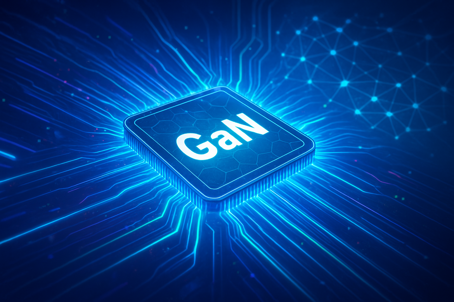
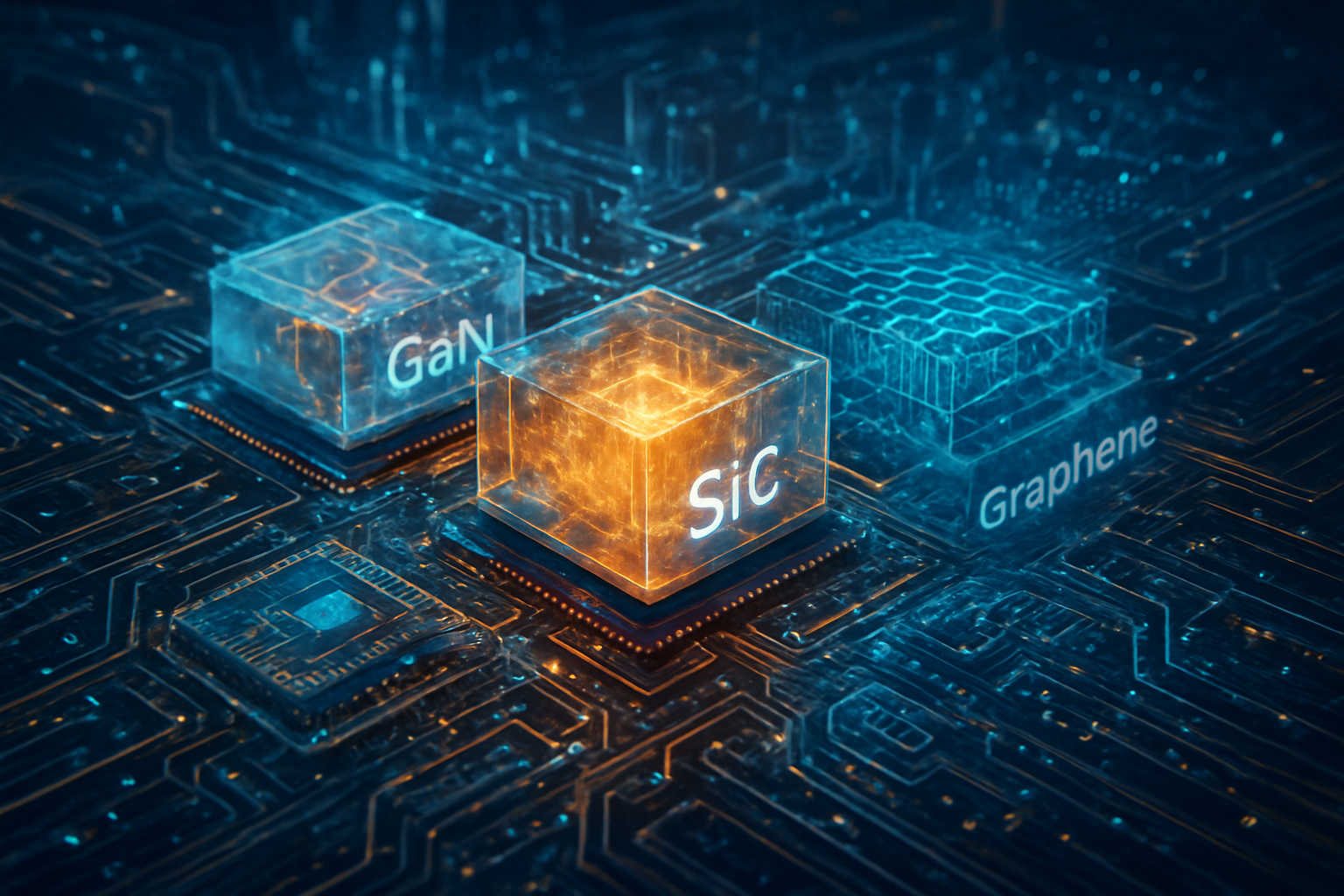
    October 20, 2025, marks a pivotal moment in semiconductor manufacturing, where a confluence of groundbreaking new tools and refined processes is propelling chip performance and efficiency to unprecedented levels. At the forefront of this revolution is the accelerated adoption of wide bandgap (WBG) compound semiconductors like Gallium Nitride (GaN) and Silicon Carbide (SiC). These materials are not merely incremental upgrades; they offer superior operating temperatures, higher breakdown voltages, and significantly faster switching speeds—up to ten times quicker than traditional silicon. This leap is critical for meeting the escalating demands of artificial intelligence (AI), high-performance computing (HPC), and electric vehicles (EVs), enabling vastly improved thermal management and drastically lower energy losses. Complementing these material innovations are sophisticated manufacturing techniques, including advanced lithography with High-NA EUV systems and revolutionary packaging solutions like die-to-wafer hybrid bonding and chiplet architectures, which integrate diverse functionalities into single, dense modules.

    Among the critical processes enabling these high-performance chips is the refinement of gold deplating, particularly relevant for the intricate fabrication of wide bandgap compound semiconductors. Gold remains an indispensable material in semiconductor devices due to its exceptional electrical conductivity, resistance to corrosion, and thermal properties, essential for contacts, vias, connectors, and bond pads. Electrolytic gold deplating has emerged as a cost-effective and precise method for "feature isolation"—the removal of the original gold seed layer after electrodeposition. This process offers significant advantages over traditional dry etch methods by producing a smoother gold surface with minimal critical dimension (CD) loss. Furthermore, innovations in gold etchant solutions, such as MacDermid Alpha's non-cyanide MICROFAB AU100 CT DEPLATE, provide precise and uniform gold seed etching on various barriers, optimizing cost efficiency and performance in compound semiconductor fabrication. These advancements in gold processing are crucial for ensuring the reliability and performance of next-generation WBG devices, directly contributing to the development of more powerful and energy-efficient electronic systems.

    The Technical Edge: Precision in a Nanometer World

    The technical advancements in semiconductor manufacturing, particularly concerning WBG compound semiconductors like GaN and SiC, are significantly enhancing efficiency and performance, driven by the insatiable demand for advanced AI and 5G technologies. A key development is the emergence of advanced gold deplating techniques, which offer superior alternatives to traditional methods for critical feature isolation in chip fabrication. These innovations are being met with strong positive reactions from both the AI research community and industry experts, who see them as foundational for the next generation of computing.

    Gold deplating is a process for precisely removing gold from specific areas of a semiconductor wafer, crucial for creating distinct electrical pathways and bond pads. Traditionally, this feature isolation was often performed using expensive dry etch processes in vacuum chambers, which could lead to roughened surfaces and less precise feature definition. In contrast, new electrolytic gold deplating tools, such as the ACM Research (NASDAQ: ACMR) Ultra ECDP and ClassOne Technology's Solstice platform with its proprietary Gen4 ECD reactor, utilize wet processing to achieve extremely uniform removal, minimal critical dimension (CD) loss, and exceptionally smooth gold surfaces. These systems are compatible with various wafer sizes (e.g., 75-200mm, configurable for non-standard sizes up to 200mm) and materials including Silicon, GaAs, GaN on Si, GaN on Sapphire, and Sapphire, supporting applications like microLED bond pads, VCSEL p- and n-contact plating, and gold bumps. The Ultra ECDP specifically targets electrochemical wafer-level gold etching outside the pattern area, ensuring improved uniformity, smaller undercuts, and enhanced gold line appearance. These advancements represent a shift towards more cost-effective and precise manufacturing, as gold is a vital material for its high conductivity, corrosion resistance, and malleability in WBG devices.

    The AI research community and industry experts have largely welcomed these advancements with enthusiasm, recognizing their pivotal role in enabling more powerful and efficient AI systems. Improved semiconductor manufacturing processes, including precise gold deplating, directly facilitate the creation of larger and more capable AI models by allowing for higher transistor density and faster memory access through advanced packaging. This creates a "virtuous cycle," where AI demands more powerful chips, and advanced manufacturing processes, sometimes even aided by AI, deliver them. Companies like Taiwan Semiconductor Manufacturing Company (TSMC) (NYSE: TSM), Intel (NASDAQ: INTC), and Samsung Electronics (KRX: 005930) are at the forefront of adopting these AI-driven innovations for yield optimization, predictive maintenance, and process control. Furthermore, the adoption of gold deplating in WBG compound semiconductors is critical for applications in electric vehicles, 5G/6G communication, RF, and various AI applications, which require superior performance in high-power, high-frequency, and high-temperature environments. The shift away from cyanide-based gold processes towards more environmentally conscious techniques also addresses growing sustainability concerns within the industry.

    Industry Shifts: Who Benefits from the Golden Age of Chips

    The latest advancements in semiconductor manufacturing, particularly focusing on new tools and processes like gold deplating for wide bandgap (WBG) compound semiconductors, are poised to significantly impact AI companies, tech giants, and startups. Gold is a crucial component in advanced semiconductor packaging due to its superior conductivity and corrosion resistance, and its demand is increasing with the rise of AI and premium smartphones. Processes like gold deplating, or electrochemical etching, are essential for precision in manufacturing, enhancing uniformity, minimizing undercuts, and improving the appearance of gold lines in advanced devices. These improvements are critical for wide bandgap semiconductors such as Silicon Carbide (SiC) and Gallium Nitride (GaN), which are vital for high-performance computing, electric vehicles, 5G/6G communication, and AI applications. Companies that successfully implement these AI-driven innovations stand to gain significant strategic advantages, influencing market positioning and potentially disrupting existing product and service offerings.

    AI companies and tech giants, constantly pushing the boundaries of computational power, stand to benefit immensely from these advancements. More efficient manufacturing processes for WBG semiconductors mean faster production of powerful and accessible AI accelerators, GPUs, and specialized processors. This allows companies like NVIDIA (NASDAQ: NVDA), Advanced Micro Devices (NASDAQ: AMD), and Qualcomm (NASDAQ: QCOM) to bring their innovative AI hardware to market more quickly and at a lower cost, fueling the development of even more sophisticated AI models and autonomous systems. Furthermore, AI itself is being integrated into semiconductor manufacturing to optimize design, streamline production, automate defect detection, and refine supply chain management, leading to higher efficiency, reduced costs, and accelerated innovation. Companies like Taiwan Semiconductor Manufacturing Company (TSMC) (NYSE: TSM), Intel (NASDAQ: INTC), and Samsung Electronics (KRX: 005930) are key players in this manufacturing evolution, leveraging AI to enhance their processes and meet the surging demand for AI chips.

    The competitive implications are substantial. Major AI labs and tech companies that can secure access to or develop these advanced manufacturing capabilities will gain a significant edge. The ability to produce more powerful and reliable WBG semiconductors more efficiently can lead to increased market share and strategic advantages. For instance, ACM Research (NASDAQ: ACMR), with its newly launched Ultra ECDP Electrochemical Deplating tool, is positioned as a key innovator in addressing challenges in the growing compound semiconductor market. Technic Inc. and MacDermid are also significant players in supplying high-performance gold plating solutions. Startups, while facing higher barriers to entry due to the capital-intensive nature of advanced semiconductor manufacturing, can still thrive by focusing on specialized niches or developing innovative AI applications that leverage these new, powerful chips. The potential disruption to existing products and services is evident: as WBG semiconductors become more widespread and cost-effective, they will enable entirely new categories of high-performance, energy-efficient AI products and services, potentially rendering older, less efficient silicon-based solutions obsolete in certain applications. This creates a virtuous cycle where advanced manufacturing fuels AI development, which in turn demands even more sophisticated chips.

    Broader Implications: Fueling AI's Exponential Growth

    The latest advancements in semiconductor manufacturing, particularly those focusing on new tools and processes like gold deplating for wide bandgap (WBG) compound semiconductors, are fundamentally reshaping the technological landscape as of October 2025. The insatiable demand for processing power, largely driven by the exponential growth of Artificial Intelligence (AI), is creating a symbiotic relationship where AI both consumes and enables the next generation of chip fabrication. Leading foundries like TSMC (NYSE: TSM) are spearheading massive expansion efforts to meet the escalating needs of AI, with 3nm and emerging 2nm process nodes at the forefront of current manufacturing capabilities. High-NA EUV lithography, capable of patterning features 1.7 times smaller and nearly tripling density, is becoming indispensable for these advanced nodes. Additionally, advancements in 3D stacking and hybrid bonding are allowing for greater integration and performance in smaller footprints. WBG semiconductors, such as GaN and SiC, are proving crucial for high-efficiency power converters, offering superior properties like higher operating temperatures, breakdown voltages, and significantly faster switching speeds—up to ten times quicker than silicon, translating to lower energy losses and improved thermal management for power-hungry AI data centers and electric vehicles.

    Gold deplating, a less conventional but significant process, plays a role in achieving precise feature isolation in semiconductor devices. While dry etch methods are available, electrolytic gold deplating offers a lower-cost alternative with minimal critical dimension (CD) loss and a smoother gold surface, integrating seamlessly with advanced plating tools. This technique is particularly valuable in applications requiring high reliability and performance, such as connectors and switches, where gold's excellent electrical conductivity, corrosion resistance, and thermal conductivity are essential. Gold plating also supports advancements in high-frequency operations and enhanced durability by protecting sensitive components from environmental factors. The ability to precisely control gold deposition and removal through deplating could optimize these connections, especially critical for the enhanced performance characteristics of WBG devices, where gold has historically been used for low inductance electrical connections and to handle high current densities in high-power circuits.

    The significance of these manufacturing advancements for the broader AI landscape is profound. The ability to produce faster, smaller, and more energy-efficient chips is directly fueling AI's exponential growth across diverse fields, including generative AI, edge computing, autonomous systems, and high-performance computing. AI models are becoming more complex and data-hungry, demanding ever-increasing computational power, and advanced semiconductor manufacturing creates a virtuous cycle where more powerful chips enable even more sophisticated AI. This has led to a projected AI chip market exceeding $150 billion in 2025. Compared to previous AI milestones, the current era is marked by AI enabling its own acceleration through more efficient hardware production. While past breakthroughs focused on algorithms and data, the current period emphasizes the crucial role of hardware in running increasingly complex AI models. The impact is far-reaching, enabling more realistic simulations, accelerating drug discovery, and advancing climate modeling. Potential concerns include the increasing cost of developing and manufacturing at advanced nodes, a persistent talent gap in semiconductor manufacturing, and geopolitical tensions that could disrupt supply chains. There are also environmental considerations, as chip manufacturing is highly energy and water intensive, and involves hazardous chemicals, though efforts are being made towards more sustainable practices, including recycling and renewable energy integration.

    The Road Ahead: What's Next for Chip Innovation

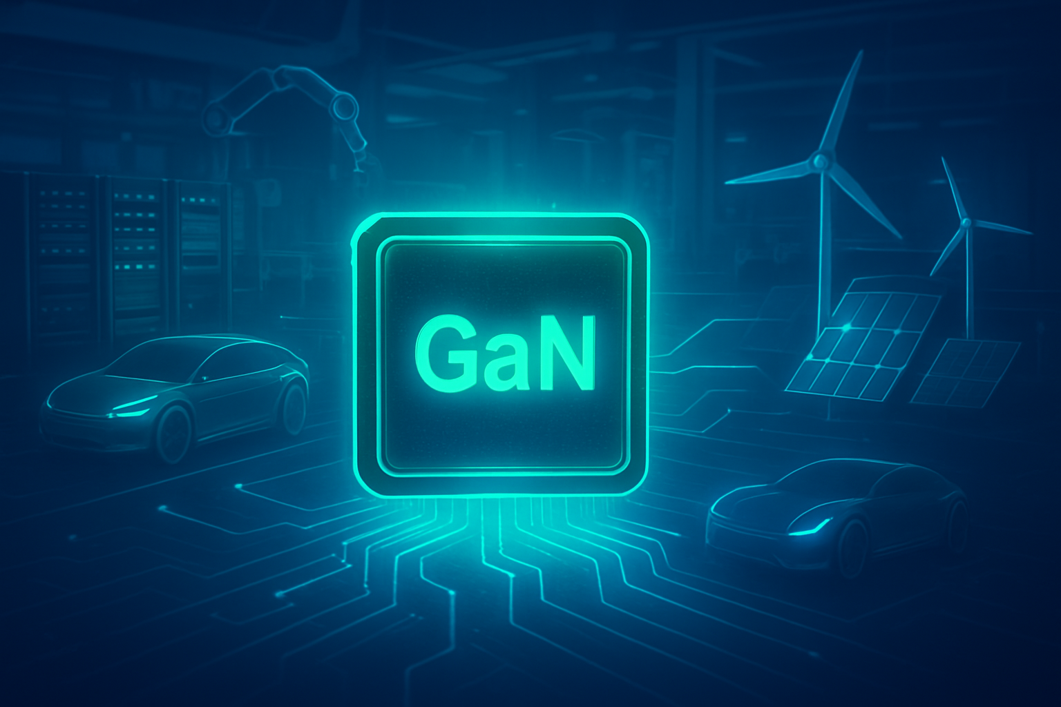
    Future developments in advanced semiconductor manufacturing are characterized by a relentless pursuit of higher performance, increased efficiency, and greater integration, particularly driven by the burgeoning demands of artificial intelligence (AI), high-performance computing (HPC), and electric vehicles (EVs). A significant trend is the move towards wide bandgap (WBG) compound semiconductors like Silicon Carbide (SiC) and Gallium Nitride (GaN), which offer superior thermal conductivity, breakdown voltage, and energy efficiency compared to traditional silicon. These materials are revolutionizing power electronics for EVs, renewable energy systems, and 5G/6G infrastructure. To meet these demands, new tools and processes are emerging, such as advanced packaging techniques, including 2.5D and 3D integration, which enable the combination of diverse chiplets into a single, high-density module, thus extending the "More than Moore" era. Furthermore, AI-driven manufacturing processes are becoming crucial for optimizing chip design and production, improving efficiency, and reducing errors in increasingly complex fabrication environments.

    A notable recent development in this landscape is the introduction of specialized tools for gold deplating, particularly for wide bandgap compound semiconductors. As of September 2025, ACM Research (NASDAQ: ACMR) launched its Ultra ECDP (Electrochemical Deplating) tool, specifically designed for wafer-level gold etching in the manufacturing of wide bandgap compound semiconductors like SiC and Gallium Arsenide (GaAs). This tool enhances electrochemical gold etching by improving uniformity, minimizing undercut, and refining the appearance of gold lines, addressing critical challenges associated with gold's use in these advanced devices. Gold is an advantageous material for these devices due to its high conductivity, corrosion resistance, and malleability, despite presenting etching and plating challenges. The Ultra ECDP tool supports processes like gold bump removal and thin film gold etching, integrating advanced features such as cleaning chambers and multi-anode technology for precise control and high surface finish. This innovation is vital for developing high-performance, energy-efficient chips that are essential for next-generation applications.

    Looking ahead, near-term developments (late 2025 into 2026) are expected to see widespread adoption of 2nm and 1.4nm process nodes, driven by Gate-All-Around (GAA) transistors and High-NA EUV lithography, yielding incredibly powerful AI accelerators and CPUs. Advanced packaging will become standard for high-performance chips, integrating diverse functionalities into single modules. Long-term, the semiconductor market is projected to reach a $1 trillion valuation by 2030, fueled by demand from high-performance computing, memory, and AI-driven technologies. Potential applications on the horizon include the accelerated commercialization of neuromorphic chips for embedded AI in IoT devices, smart sensors, and advanced robotics, benefiting from their low power consumption. Challenges that need addressing include the inherent complexity of designing and integrating diverse components in heterogeneous integration, the lack of industry-wide standardization, effective thermal management, and ensuring material compatibility. Additionally, the industry faces persistent talent gaps, supply chain vulnerabilities exacerbated by geopolitical tensions, and the critical need for sustainable manufacturing practices, including efficient gold recovery and recycling from waste. Experts predict continued growth, with a strong emphasis on innovations in materials, advanced packaging, and AI-driven manufacturing to overcome these hurdles and enable the next wave of technological breakthroughs.

    A New Era for AI Hardware: The Golden Standard

    The semiconductor manufacturing landscape is undergoing a rapid transformation driven by an insatiable demand for more powerful, efficient, and specialized chips, particularly for artificial intelligence (AI) applications. As of October 2025, several cutting-edge tools and processes are defining this new era. Extreme Ultraviolet (EUV) lithography continues to advance, enabling the creation of features as small as 7nm and below with fewer steps, boosting resolution and efficiency in wafer fabrication. Beyond traditional scaling, the industry is seeing a significant shift towards "more than Moore" approaches, emphasizing advanced packaging technologies like CoWoS, SoIC, hybrid bonding, and 3D stacking to integrate multiple components into compact, high-performance systems. Innovations such as Gate-All-Around (GAA) transistor designs are entering production, with TSMC (NYSE: TSM) and Intel (NASDAQ: INTC) slated to scale these in 2025, alongside backside power delivery networks that promise reduced heat and enhanced performance. AI itself is becoming an indispensable tool within manufacturing, optimizing quality control, defect detection, process optimization, and even chip design through AI-driven platforms that significantly reduce development cycles and improve wafer yields.

    A particularly noteworthy advancement for wide bandgap compound semiconductors, critical for electric vehicles, 5G/6G communication, RF, and AI applications, is the emergence of advanced gold deplating processes. In September 2025, ACM Research (NASDAQ: ACMR) launched its Ultra ECDP Electrochemical Deplating tool, specifically engineered for electrochemical wafer-level gold (Au) etching in the manufacturing of these specialized semiconductors. Gold, prized for its high conductivity, corrosion resistance, and malleability, presents unique etching and plating challenges. The Ultra ECDP tool tackles these by offering improved uniformity, smaller undercuts, enhanced gold line appearance, and specialized processes for Au bump removal, thin film Au etching, and deep-hole Au deplating. This precision technology is crucial for optimizing devices built on substrates like silicon carbide (SiC) and gallium arsenide (GaAs), ensuring superior electrical conductivity and reliability in increasingly miniaturized and high-performance components. The integration of such precise deplating techniques underscores the industry's commitment to overcoming material-specific challenges to unlock the full potential of advanced materials.

    The significance of these developments in AI history is profound, marking a defining moment where hardware innovation directly dictates the pace and scale of AI progress. These advancements are the fundamental enablers for the ever-increasing computational demands of large language models, advanced computer vision, and sophisticated reinforcement learning, propelling AI into truly ubiquitous applications from hyper-personalized edge devices to entirely new autonomous systems. The long-term impact points towards a global semiconductor market projected to exceed $1 trillion by 2030, potentially reaching $2 trillion by 2040, driven by this symbiotic relationship between AI and semiconductor technology. Key takeaways include the relentless push for miniaturization to sub-2nm nodes, the indispensable role of advanced packaging, and the critical need for energy-efficient designs as power consumption becomes a growing concern. In the coming weeks and months, industry observers should watch for the continued ramp-up of next-generation AI chip production, such as Nvidia's (NASDAQ: NVDA) Blackwell wafers in the US, the further progress of Intel's (NASDAQ: INTC) 18A process, and TSMC's (NYSE: TSM) accelerated capacity expansions driven by strong AI demand. Additionally, developments from emerging players in advanced lithography and the broader adoption of chiplet architectures, especially in demanding sectors like automotive, will be crucial indicators of the industry's trajectory.


    This content is intended for informational purposes only and represents analysis of current AI developments.

    TokenRing AI delivers enterprise-grade solutions for multi-agent AI workflow orchestration, AI-powered development tools, and seamless remote collaboration platforms.
    For more information, visit https://www.tokenring.ai/.