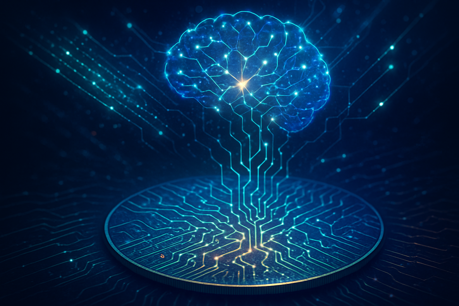
The creative industries stand on the precipice of a monumental transformation, driven by the relentless march of artificial intelligence. From the visionary predictions of legendary game designer Hideo Kojima regarding AI's role in crafting future remakes and sequels, to World Wrestling Entertainment's (NYSE: TKO) reported ventures into AI-generated storylines, the landscape of artistic creation is undergoing a profound redefinition. These developments signal a dual narrative: one of unprecedented efficiency and innovation, and another fraught with ethical dilemmas and the potential for creative commodification.
The Technical Canvas: AI as Co-Creator and Story Engine
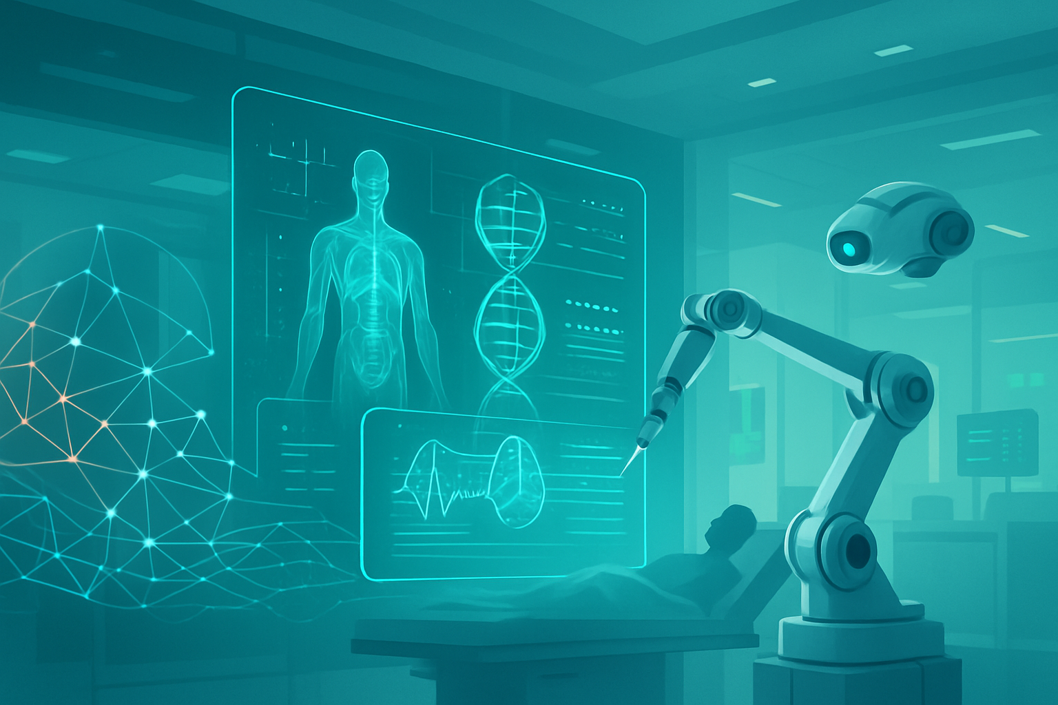
Hideo Kojima, the acclaimed mind behind Metal Gear Solid and Death Stranding, envisions AI as a supportive "friend" in game development, not a replacement for human ingenuity. He posits that AI will primarily tackle "tedious tasks" – the repetitive, labor-intensive aspects of game creation – thereby significantly boosting efficiency and reducing development costs and timelines. This liberation of human talent, Kojima argues, will allow creators to focus on pioneering entirely new intellectual properties and pushing the boundaries of interactive storytelling. He explicitly predicts a future where "remakes and sequels will be made by AI," leveraging existing game data and structures to streamline their production. AI's capabilities in this context would include advanced procedural content generation for environments and assets, character likeness generation and refinement (as seen in early experiments for Death Stranding 2), and optimizing various workflow processes. This approach starkly contrasts traditional game development, where remakes and sequels demand extensive human effort for asset recreation and narrative adaptation.
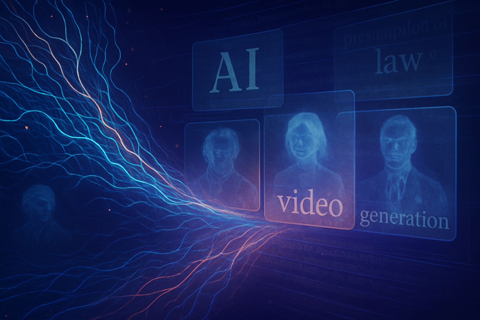
Meanwhile, World Wrestling Entertainment (NYSE: TKO) is reportedly experimenting with an AI platform, identified as "Writer AI" or Writer Inc., to generate wrestling storylines. This initiative, spearheaded by Senior Director of Creative Strategy Cyrus Kowsari under the direction of Chief Content Officer Paul "Triple H" Levesque, aims to integrate AI into storytelling, video production, and graphics. The reported capabilities of this AI include generating basic narrative outlines, suggesting match scenarios, and even bullet points for character promos. However, initial results have been famously described as "absurdly bad," with one notable pitch involving former WWE star Bobby Lashley returning as a character obsessed with Japanese culture and history. This highlights the AI's current limitations: a struggle with nuance, emotional depth, established character continuity, and the inherent improvisational nature crucial to compelling professional wrestling. Unlike traditional wrestling creative teams who deeply understand character psychology, long-term booking, and audience reactions, current AI output often lacks the human touch required for truly engaging, emotionally resonant narratives.
Corporate Playbook: Shifting Sands for Tech Giants and Startups
The embrace of AI by figures like Kojima and entities like WWE presents a massive opportunity for various players in the AI ecosystem. Generative AI model developers, such as those creating foundational text-to-image, text-to-video, and large language models, will become crucial suppliers. Companies offering AI-powered development tools, like PrometheanAI Inc. and Inworld AI, which integrate AI for game design and asset creation, are poised for increased adoption. Furthermore, providers of personalization and adaptive content platforms will be highly sought after as the demand for dynamic, tailored user experiences grows. Cloud infrastructure giants like Amazon (NASDAQ: AMZN) AWS, Microsoft (NASDAQ: MSFT) Azure, and Alphabet's (NASDAQ: GOOGL) Google Cloud will also see significant benefits from the increased computational demands of training and deploying these large AI models.
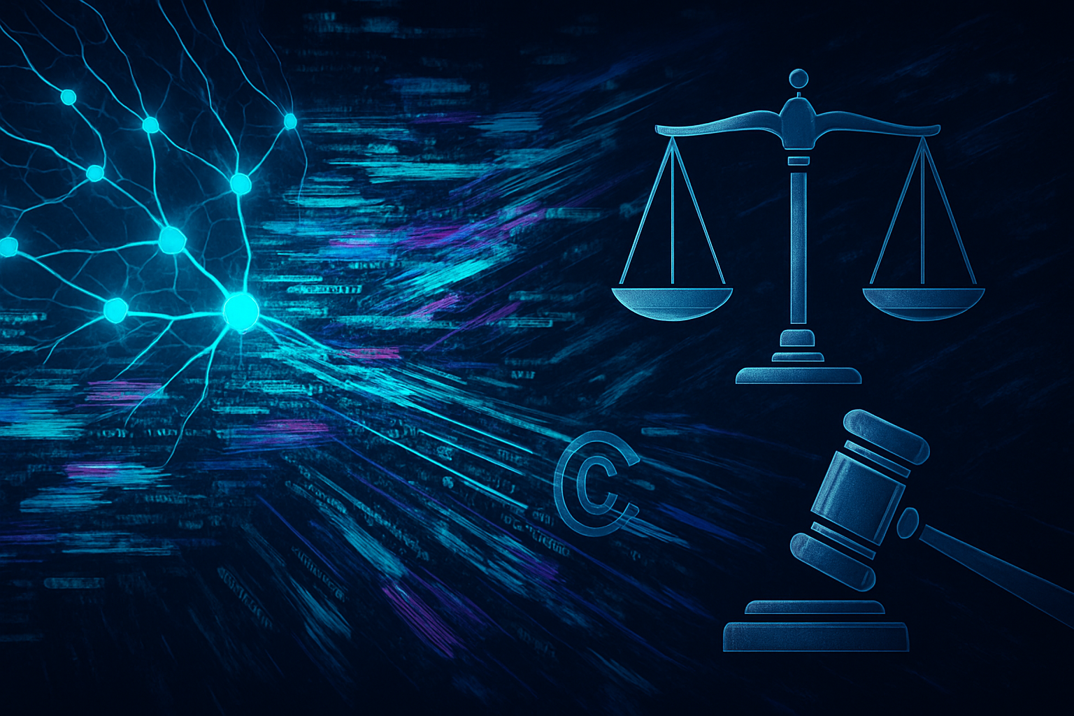
Competitive implications for major AI labs and tech companies are intensifying. Access to vast, diverse, and ethically sourced datasets of creative content will become a critical competitive advantage, although this raises significant intellectual property (IP) and copyright concerns. The demand for AI research talent and engineers specializing in creative applications will surge, leading to a "talent war." Tech giants may strategically acquire promising AI startups to integrate innovative tools and expand their market reach. Companies prioritizing ethical AI development and offering "human-in-the-loop" solutions that augment, rather than replace, human creativity are likely to build stronger relationships with creators and gain a strategic edge. This disruption could redefine existing products and services, as traditional software for 3D modeling, animation, and even entry-level scriptwriting may need to integrate AI features or risk obsolescence.
Wider Resonance: Societal Impacts and Ethical Crossroads
These developments fit into a broader AI landscape characterized by the proliferation of generative AI tools that are democratizing content creation. AI is no longer merely automating tasks but actively reshaping how professionals ideate, produce, and distribute content across design, photography, video, music, and writing. The conversation is increasingly focused on balancing innovation with ethical responsibility.
However, this rapid integration brings forth a complex array of societal impacts and concerns. A significant fear among creative professionals is job displacement, with AI tools being cheaper, faster, and increasingly sophisticated. This can lead to a reduction in the financial value attributed to creative work, particularly affecting freelancers and self-employed individuals. Ethical considerations are paramount, especially regarding copyright infringement from AI models trained on unauthorized works, and the ownership of AI-generated content. Bias within training data can also lead to AI-generated content that perpetuates stereotypes. Furthermore, concerns about creative integrity and authenticity arise, as AI-generated content, while technically proficient, can often lack the emotional depth, unique voice, and cultural nuances that human creators bring. The proliferation of AI-generated content could "flood" the market, making it harder for emerging artists to stand out.
Historically, technological advancements in art, such as the advent of photography, initially sparked fears of displacement but ultimately led to new art forms. Today, AI presents a similar paradigm shift, pushing the boundaries of what is considered "art" and redefining the roles of human creators. The challenge lies in harnessing AI's potential to augment creativity while establishing robust ethical frameworks and legal protections.
The Horizon: Future Developments and Expert Predictions
In the near term (1-3 years), expect to see enhanced human-AI collaboration, with creatives using AI as a "co-pilot" for brainstorming, rapid prototyping, and automating mundane tasks like initial asset generation and basic editing. This will lead to increased efficiency and cost reduction, with niche AI tools becoming more stable and seamlessly integrated into workflows. Personalization will continue to advance, offering increasingly tailored content experiences.
Longer term (3+ years), the line between human and AI creativity may blur further, with the potential for entirely AI-produced films, music albums, or games becoming more mainstream. AI could handle up to 90% of the work for game remakes and sequels, including retexturing assets, composing new music, and redoing voice work. New art forms and interactive experiences will emerge, with AI enabling dynamic, adaptive content that changes in real-time based on user interaction or emotional response. Creative roles will evolve, with "creative orchestration" – directing multiple AI agents – becoming a fundamental skill.
Challenges will persist, particularly around authorship and copyright, job displacement, and ensuring AI-generated content maintains human nuance and originality. Quality control will remain crucial, as current AI models can "hallucinate" or fabricate information, leading to absurd outputs. Experts predict a future where AI augments human capabilities, leading to hybrid workflows and a demand for "AI orchestrators." The World Economic Forum suggests AI will augment existing jobs and create new ones, though some foresee a polarization within the creative industry.
The Final Act: A Transformative Era Unfolds
The ventures of Hideo Kojima and WWE into AI-driven creation represent a pivotal moment in AI history, moving beyond theoretical discussions to practical, albeit sometimes flawed, integration into highly subjective creative domains. Kojima's nuanced perspective advocates for a symbiotic relationship, where AI enhances efficiency and frees human ingenuity for innovation. WWE's aggressive push, despite early "absurdly bad" results, highlights a willingness of major entertainment entities to strategically embrace AI, even for core creative functions. This marks a shift from AI as a mere backend utility to a front-facing content-generating force, fundamentally testing the boundaries of "creativity" and "authorship."
The long-term impact will likely see AI excel at generating vast volumes of derivative, optimized, or "tedious" content, allowing human creators to focus on original concepts and deeply emotional storytelling. The "democratization" of creative tools will continue, leading to an explosion of diverse content, but also a potential flood of low-quality, AI-generated material. Ethical and legal frameworks around AI, especially concerning intellectual property and fair compensation for creators whose work trains AI models, will be critical. The emergence of "walled garden" LLMs, trained on proprietary, cleared content, is a significant trend to watch for mitigating legal risks. Job roles will undoubtedly evolve; with new positions focused on AI prompt engineering, supervision, and innovative human-AI collaboration emerging. The ultimate goal should be to leverage AI to enhance human expression and experience, rather than diminish it, ensuring that technology remains in service to meaningful storytelling and artistic vision.
What to watch for in the coming weeks and months:
- WWE's AI Storyline Evolution: Keep an eye on how WWE refines its "Writer AI" platform. Will the quality of AI-generated pitches improve? Will there be specific segments or characters overtly attributed to AI influence (even subtly)? How will this impact audience reception and talent morale?
- Legal Precedents: Look for ongoing discussions, new legislation (like the EU's AI Act), and court cases addressing AI copyright, authorship, and fair use.
- "Walled Garden" LLMs: Observe the development and adoption of proprietary AI models by major studios and entertainment companies, such as Lionsgate's partnership with Runway AI.
- Specialized AI Tools: Expect to see further development and increased stability in niche, use-case-specific AI tools for various creative tasks, becoming more integrated into standard production pipelines.
- New Collaborative Roles: Watch for the emergence of new job titles and skill sets that bridge human creativity with AI capabilities.
- Public and Creator Sentiment: Monitor public and creator sentiment towards AI-generated content. Continued instances of "poorly rendered" or "creatively bankrupt" AI output could lead to stronger calls for human-led creative integrity.
This content is intended for informational purposes only and represents analysis of current AI developments.
TokenRing AI delivers enterprise-grade solutions for multi-agent AI workflow orchestration, AI-powered development tools, and seamless remote collaboration platforms.
For more information, visit https://www.tokenring.ai/.