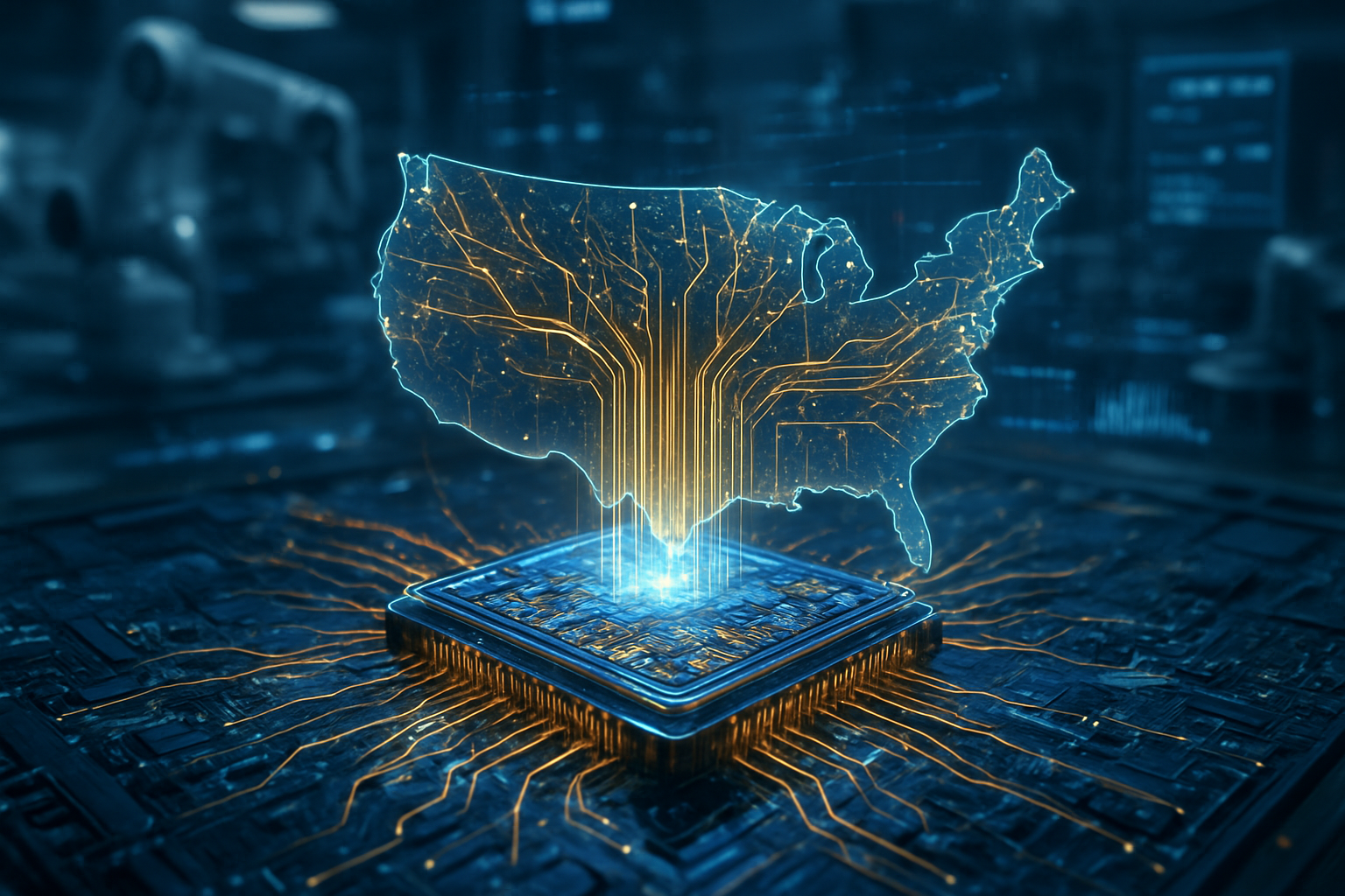
In a move that underscores the insatiable appetite for artificial intelligence infrastructure, ByteDance, the parent company of TikTok, has reportedly finalized a staggering $14.3 billion (100 billion yuan) order for high-performance AI chips from NVIDIA (NASDAQ: NVDA). This procurement, earmarked for the 2026 fiscal year, represents a significant escalation from the $12 billion the social media giant spent in 2025. The deal signals ByteDance's determination to maintain its lead in the generative AI space, even as geopolitical tensions and complex export regulations reshape the silicon landscape.
The scale of this order reflects more than just a corporate expansion; it highlights a critical inflection point in the global AI race. As ByteDance’s "Doubao" large language model (LLM) reaches a record-breaking processing volume of over 50 trillion tokens daily, the company’s need for raw compute has outpaced its domestic alternatives. This massive investment not only bolsters NVIDIA's dominant market position but also serves as a litmus test for the "managed access" trade policies currently governing the flow of advanced technology between the United States and China.
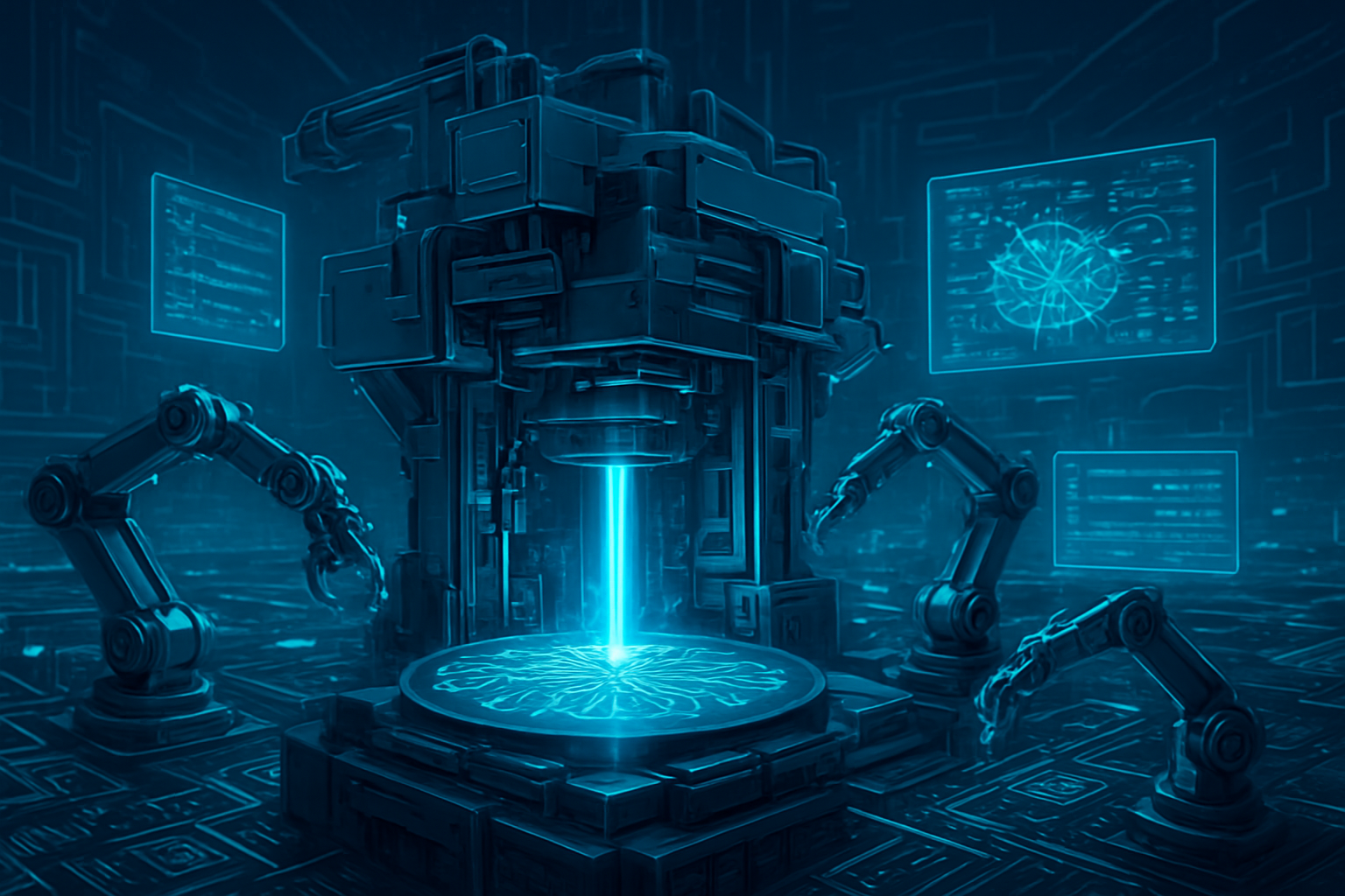
The Technical Frontier: H200s, Blackwell Variants, and the 25% Surcharge
At the heart of ByteDance’s $14.3 billion procurement is a sophisticated mix of hardware designed to navigate the tightening web of U.S. export controls. The primary focus for 2026 is the NVIDIA H200, a powerhouse based on the Hopper architecture. Unlike the previous "China-specific" H20 models, which were heavily throttled to meet regulatory caps, the H200 offers nearly six times the computing power and features 141GB of high-bandwidth memory (HBM3E). This marks a strategic shift in U.S. policy, which now allows the export of these more capable chips to "approved" Chinese entities, provided they pay a 25% federal surcharge—a move intended to fund domestic American semiconductor reshoring projects.
Beyond the H200, NVIDIA is reportedly readying "cut-down" versions of its flagship Blackwell architecture, tentatively dubbed the B20 and B30A. These chips are engineered to deliver superior performance to the aging H20 while remaining within the strict memory bandwidth and FLOPS limits set by the U.S. Department of Commerce. While the top-tier Blackwell B200 and the upcoming Rubin R100 series remain strictly off-limits to Chinese firms, the B30A is rumored to offer up to double the inference performance of current compliant models. This tiered approach allows NVIDIA to monetize its cutting-edge R&D in a restricted market without crossing the "red line" of national security.
To hedge against future regulatory shocks, ByteDance is not relying solely on NVIDIA. The company has intensified its partnership with Broadcom (NASDAQ: AVGO) and TSMC (NYSE: TSM) to develop custom internal AI chips. These bespoke processors, expected to debut in mid-2026, are specifically designed for "inference" tasks—running the daily recommendation algorithms for TikTok and Douyin. By offloading these routine tasks to in-house silicon, ByteDance can reserve its precious NVIDIA H200 clusters for the more demanding process of training its next-generation LLMs, ensuring that its algorithmic "secret sauce" continues to evolve at breakneck speeds.
Shifting Tides: Competitive Fallout and Market Positioning
The financial implications of this deal are reverberating across Wall Street. NVIDIA stock, which has seen heightened volatility in early 2026, reacted with cautious optimism. While the $14 billion order provides a massive revenue floor, analysts from firms like Wedbush note that the 25% surcharge and the "U.S. Routing" verification rules introduce new margin pressures. If NVIDIA is forced to absorb part of the "Silicon Surcharge" to remain competitive against domestic Chinese challengers, its industry-leading gross margins could face their first real test in years.
In China, the deal has created a "paradox of choice" for other tech titans like Alibaba (NYSE: BABA) and Tencent (OTC: TCEHY). These companies are closely watching ByteDance’s move as they balance government pressure to use "national champions" like Huawei against the undeniable performance advantages of NVIDIA’s CUDA ecosystem. Huawei’s latest Ascend 910C chip, while impressive, is estimated to deliver only 60% to 80% of the raw performance of an NVIDIA H100. For a company like ByteDance, which operates the world’s most popular recommendation engine, that performance gap is the difference between a seamless user experience and a platform-killing lag.
The move also places immense pressure on traditional cloud providers and hardware manufacturers. Companies like Intel (NASDAQ: INTC), which are benefiting from the U.S. government's re-investment of the 25% surcharge, find themselves in a race to prove they can build the "domestic AI foundry" of the future. Meanwhile, in the consumer sector, the sheer compute power ByteDance is amassing is expected to trickle down into its commercial partnerships. Automotive giants such as Mercedes-Benz (OTC: MBGYY) and BYD (OTC: BYDDY), which utilize ByteDance’s Volcano Engine cloud services, will likely see a significant boost in their own AI-driven autonomous driving and in-car assistant capabilities as a direct result of this hardware influx.
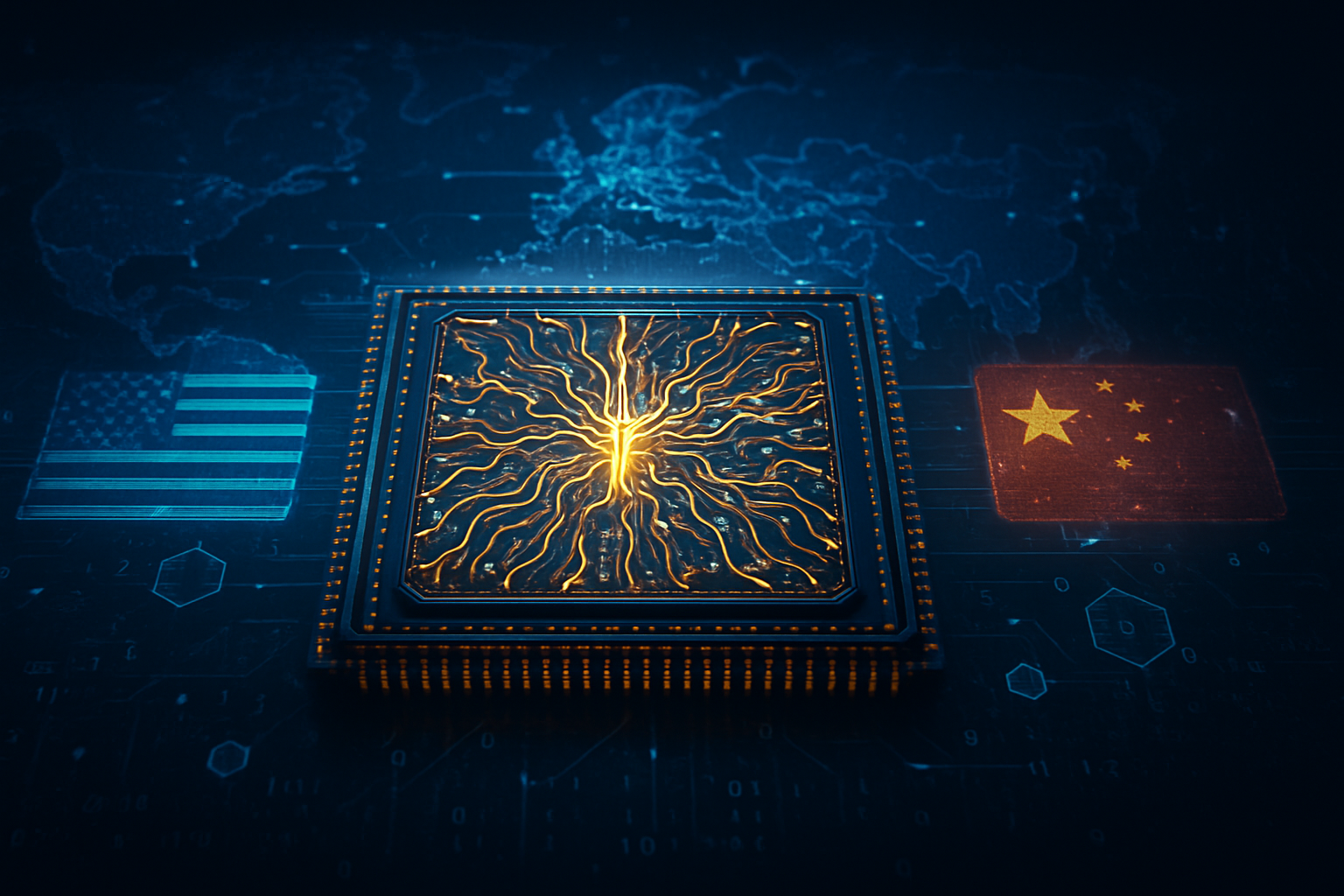
The "Silicon Curtain" and the Global Compute Gap
The $14 billion order is a defining moment in what experts are calling the "Silicon Curtain"—a technological divide separating Western and Eastern AI ecosystems. By allowing the H200 to enter China under a high-tariff regime, the U.S. is essentially treating AI chips as a strategic commodity, similar to oil. This "taxable dependency" model allows the U.S. to monitor and slow down Chinese AI progress while simultaneously extracting the capital needed to build its own next-generation foundries.
Current projections regarding the "compute gap" between the U.S. and China suggest a widening chasm. While the H200 will help ByteDance stay competitive in the near term, the U.S. domestic market is already moving toward the Blackwell and Rubin architectures. Think tanks like the Council on Foreign Relations warn that while this $14 billion order helps Chinese firms narrow the gap from a 10x disadvantage to perhaps 5x by late 2026, the lack of access to ASML’s most advanced EUV lithography machines means that by 2027, the gap could balloon to 17x. China is effectively running a race with its shoes tied together, forced to spend more for yesterday's technology.
Furthermore, this deal has sparked a domestic debate within China. In late January 2026, reports surfaced of Chinese customs officials temporarily halting H200 shipments in Shenzhen, ostensibly to promote self-reliance. However, the eventual "in-principle approval" given to ByteDance suggests that Beijing recognizes that its "hyperscalers" cannot survive on domestic silicon alone—at least not yet. The geopolitical friction is palpable, with many viewing this massive order as a primary bargaining chip in the lead-up to the anticipated April 2026 diplomatic summit between U.S. and Chinese leadership.
Future Outlook: Beyond the 100 Billion Yuan Spend
Looking ahead, the next 18 to 24 months will be a period of intensive infrastructure building for ByteDance. The company is expected to deploy its H200 clusters across a series of new, high-efficiency data centers designed to handle the massive heat output of these advanced GPUs. Near-term applications will focus on "generative video" for TikTok, allowing users to create high-fidelity, AI-generated content in real-time. Long-term, ByteDance is rumored to be working on a "General Purpose Agent" that could handle complex personal tasks across its entire ecosystem, necessitating even more compute than currently available.
However, challenges remain. The reliance on NVIDIA’s CUDA software remains a double-edged sword. While it provides immediate performance, it also creates a "software lock-in" that makes transitioning to domestic chips like Huawei’s Ascend line incredibly difficult and costly. Experts predict that 2026 will see a massive push by the Chinese government to develop a "unified AI software layer" that could allow developers to switch between NVIDIA and domestic hardware seamlessly, though such a feat is years away from reality.
A Watershed Moment for Artificial Intelligence
NVIDIA's $14 billion deal with ByteDance is more than just a massive transaction; it is a signal of the high stakes involved in the AI era. It demonstrates that for the world’s leading tech companies, access to high-end silicon is not just a luxury—it is a survival requirement. This development highlights NVIDIA’s nearly unassailable position at the top of the AI value chain, while also revealing the deep-seated anxieties of nations and corporations alike as they navigate an increasingly fragmented global market.
In the coming months, the industry will be watching closely to see if the H200 shipments proceed without further diplomatic interference and how ByteDance’s internal chip program progresses. For now, the "Silicon Surcharge" era has officially begun, and the price of staying at the forefront of AI innovation has never been higher. As the global compute gap continues to shift, the decisions made by companies like ByteDance today will define the technological hierarchy of the next decade.
This content is intended for informational purposes only and represents analysis of current AI developments.
TokenRing AI delivers enterprise-grade solutions for multi-agent AI workflow orchestration, AI-powered development tools, and seamless remote collaboration platforms.
For more information, visit https://www.tokenring.ai/.