As the calendar turns to early 2026, the European Union is standing at a critical crossroads in its quest for technological sovereignty. The European Commission has officially initiated a high-stakes review of the European Chips Act, colloquially dubbed "Chips Act 2.0," aimed at recalibrating the bloc's ambitious goal of doubling its global semiconductor market share to 20% by 2030. This strategic pivot comes in the wake of a sobering report from the European Court of Auditors (ECA), which cautioned that Europe remains "off the pace" to meet its original targets. While the first iteration of the Act successfully catalyzed over €80 billion in investment commitments, the 2026 review marks a fundamental shift from a "quantity-first" approach to a more nuanced "value-first" strategy, prioritizing the high-tech niches that will define the next decade of artificial intelligence.
The reinvigorated strategy is born out of necessity. With the recent postponement of high-profile "mega-fab" projects, including Intel Corporation’s (NASDAQ: INTC) planned €30 billion facility in Magdeburg, Germany, EU policymakers are moving away from a singular focus on front-end logic manufacturing. Instead, the new framework seeks to build a "Silicon Shield" by dominating the specialized sectors of the supply chain where Europe already holds a competitive edge: advanced materials, innovative chip design, and next-generation packaging. By integrating these hardware advancements with the continent's rising AI software stars, Europe aims to secure its strategic autonomy in an era of intensifying geopolitical friction and rapid AI deployment.
Technical Evolution: From Mega-Fabs to Advanced Architectures
The technical core of the Chips Act 2.0 review centers on the "lab-to-fab" transition, a historical bottleneck where European research excellence failed to translate into commercial production. Central to this effort is the newly formalized RESOLVE Initiative, a coordinated accelerator focusing on 15 distinct technology tracks. Unlike previous efforts that prioritized standard silicon wafers, RESOLVE emphasizes Wide-Bandgap (WBG) materials such as Silicon Carbide (SiC) and Gallium Nitride (GaN). These materials are essential for the high-efficiency power modules required by AI data centers and electric vehicles, areas where European firms currently lead the global market.
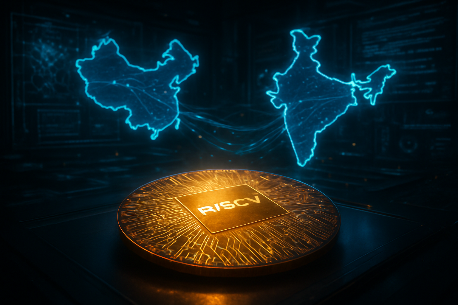
Furthermore, the 2026 strategy places a heavy technical emphasis on Advanced Packaging and 3D Heterogeneous Integration. As traditional Moore’s Law scaling becomes prohibitively expensive, the EU is betting on "chiplet" technology—combining multiple smaller chips into a single package to boost performance. The APECS program, led by the Fraunhofer Institute, is spearheading this move toward sub-5nm logic integration. Additionally, the launch of the European Design Platform (EDP) provides a cloud-based environment for startups to access expensive Electronic Design Automation (EDA) tools and IP libraries, specifically targeting the development of energy-efficient "Green AI" chips and RISC-V architectures.
This shift represents a significant departure from the 2023 approach. While the original Act chased "first-of-a-kind" leading-edge logic fabs to compete with Asia and the US, the 2.0 review recognizes that Europe’s strength lies in Edge AI and Smart Power. By focusing on Fully Depleted Silicon-on-Insulator (FD-SOI) technology—a European-pioneered process that offers superior energy efficiency for mobile and IoT devices—the EU is carving out a technical niche that is less reliant on the ultra-expensive extreme ultraviolet (EUV) lithography dominated by a few global players.
Industry Implications: Winners, Losers, and Strategic Realignment
The industry landscape in 2026 is one of stark contrasts. ASML Holding N.V. (NASDAQ: ASML) remains the undisputed kingmaker of the industry, as its lithography machines are vital for any advanced manufacturing on the continent. However, the "mega-fab" dream has faced significant headwinds. While the joint venture between Taiwan Semiconductor Manufacturing Co. (NYSE: TSM) and European partners in Dresden—the ESMC fab—remains on track for a 2027 production start, other projects have faltered. The stalling of the STMicroelectronics N.V. (NYSE: STM) and GlobalFoundries Inc. (NASDAQ: GFS) project in Crolles, France, has forced the EU to simplify state aid rules for "strategic value" projects, making it easier for smaller, more specialized facilities to receive funding.
Companies like Infineon Technologies AG (OTCMKTS: IFNNY) and NXP Semiconductors N.V. (NASDAQ: NXPI) stand to be the primary beneficiaries of the 2.0 pivot. Infineon’s new "Smart Power" fab in Dresden, scheduled to reach full scale-up by mid-2026, aligns perfectly with the EU’s focus on AI data center infrastructure. These firms are moving beyond being mere component suppliers to becoming integrated platform providers. For instance, NXP is increasingly collaborating with European AI software firms like Aleph Alpha to integrate sovereign LLMs directly into automotive edge processors, creating a vertically integrated "European AI stack" that bypasses traditional Silicon Valley dependencies.
For AI startups and "fabless" designers, the implications are transformative. The European Design Platform effectively lowers the barrier to entry for companies like Mistral AI to design custom silicon optimized for their specific models. This move disrupts the existing market dominance of general-purpose AI hardware, allowing European companies to compete on performance-per-watt metrics. By fostering a domestic ecosystem of "AI-native" hardware, the EU is attempting to shield its tech sector from the supply chain volatility and export controls that have plagued the industry over the last three years.
Strategic Autonomy and the "Green AI" Mandate
The broader significance of the Chips Act 2.0 review extends far beyond industrial policy; it is a cornerstone of Europe’s geopolitical strategy. In a world where AI compute is increasingly viewed as a national security asset, the EU’s "Silicon Shield" is designed to ensure that the continent is not merely a consumer of foreign technology. This fits into the wider trend of "de-risking" supply chains from over-reliance on a single geographic region. By building out its own AI Factories—sovereign computing hubs powered by European-designed chips—the bloc is asserting its independence in the global AI arms race.
A key differentiator for Europe is its commitment to "Green AI." The 2026 strategy explicitly links semiconductor funding to sustainability goals, prioritizing chips that minimize the massive carbon footprint of AI training and inference. This focus on energy efficiency is not just an environmental mandate but a strategic advantage in a power-constrained world. The development of silicon photonics—using light instead of electricity to move data—is a major milestone in this effort. Projects led by STMicroelectronics and various European research institutes are now moving into pilot production, promising to reduce data center energy consumption by up to 40%.
Concerns remain, however, regarding the fragmentation of EU funding. The European Court of Auditors highlighted that the vast majority of semiconductor investment still relies on the "financial muscle" of individual member states, creating a potential subsidy race between Germany, France, and Italy. Critics argue that without a more centralized "European Chips Fund," the bloc may struggle to achieve the scale necessary to truly rival the United States or China. Nevertheless, the 2026 review is a clear admission that the path to 2030 requires more than just money; it requires a cohesive technical and political vision.
The Road to 2030: Future Developments and Challenges
Looking ahead, the next 18 to 24 months will be decisive. By late 2026, the first wave of AI Factories under the EuroHPC Joint Undertaking is expected to be fully operational, providing a sovereign cloud infrastructure for European researchers. We can expect to see the first "made-for-Europe" AI accelerators emerging from the European Design Platform, potentially utilizing RISC-V architectures to avoid the licensing complexities associated with proprietary instruction sets. These chips will likely find their first major applications in the "Industrial AI" sector—automotive, smart manufacturing, and healthcare—where data privacy and reliability are paramount.
The long-term success of the 2.0 strategy will depend on addressing the chronic talent shortage in semiconductor engineering. The EU has proposed a "Chips Academy" to train 500,000 specialists by 2030, but the results of this initiative are still in their infancy. Furthermore, the industry must navigate the "valley of death" between prototype and mass production. If the RESOLVE initiative can successfully bridge this gap, Europe could become the global hub for specialized, high-efficiency AI hardware. However, if the fragmentation of funding and regulatory hurdles persist, the 20% market share goal may remain an elusive aspiration.
Conclusion: A New Era for European Tech
The EU’s Chips Act 2.0 review marks the beginning of a more mature, realistic phase of European industrial policy. By moving away from the "aspirational" targets of the past and focusing on the tangible strengths of its research and specialized manufacturing base, the Union is building a more resilient foundation for the AI era. The shift from "volume to value" is a strategic acknowledgement that Europe does not need to manufacture every chip in the world to be a global leader; it only needs to control the critical nodes of the future.
The significance of this development in AI history cannot be overstated. It represents the first major attempt by a continental power to vertically integrate AI software development with sovereign hardware manufacturing on a massive scale. As we watch the implementation of the RESOLVE initiative and the rollout of the European Design Platform in the coming months, the world will see if the "Silicon Shield" can truly protect Europe’s digital future. For now, the message from Brussels is clear: Europe is no longer content to be a spectator in the semiconductor revolution; it intends to be its architect.
This content is intended for informational purposes only and represents analysis of current AI developments.
TokenRing AI delivers enterprise-grade solutions for multi-agent AI workflow orchestration, AI-powered development tools, and seamless remote collaboration platforms. For more information, visit https://www.tokenring.ai/.