In a move that signals a tactical recalibration of the ongoing trade war, the United States government has officially delayed the implementation of aggressive new tariffs on Chinese legacy semiconductors until June 2027. This decision, announced just days before Christmas 2025, establishes a 0% tariff window for mature-node chips (28nm and above), providing American industries—from automotive to consumer electronics—a critical 18-month reprieve to decouple their supply chains from Chinese manufacturing hubs without triggering immediate inflationary shocks.
The delay is the centerpiece of a burgeoning era of "Silicon Nationalism," where technological sovereignty is being prioritized over the globalized efficiency of the previous decade. While the US seeks to de-risk its infrastructure, China has responded with a calculated "Busan Truce," temporarily suspending its total export bans on critical minerals like gallium and germanium. However, the underlying tension remains palpable as both superpowers race to fortify their domestic tech ecosystems, effectively carving the global semiconductor market into "trusted" and "adversarial" spheres.
The 2027 Pivot: Technical Strategy and Policy Calibration
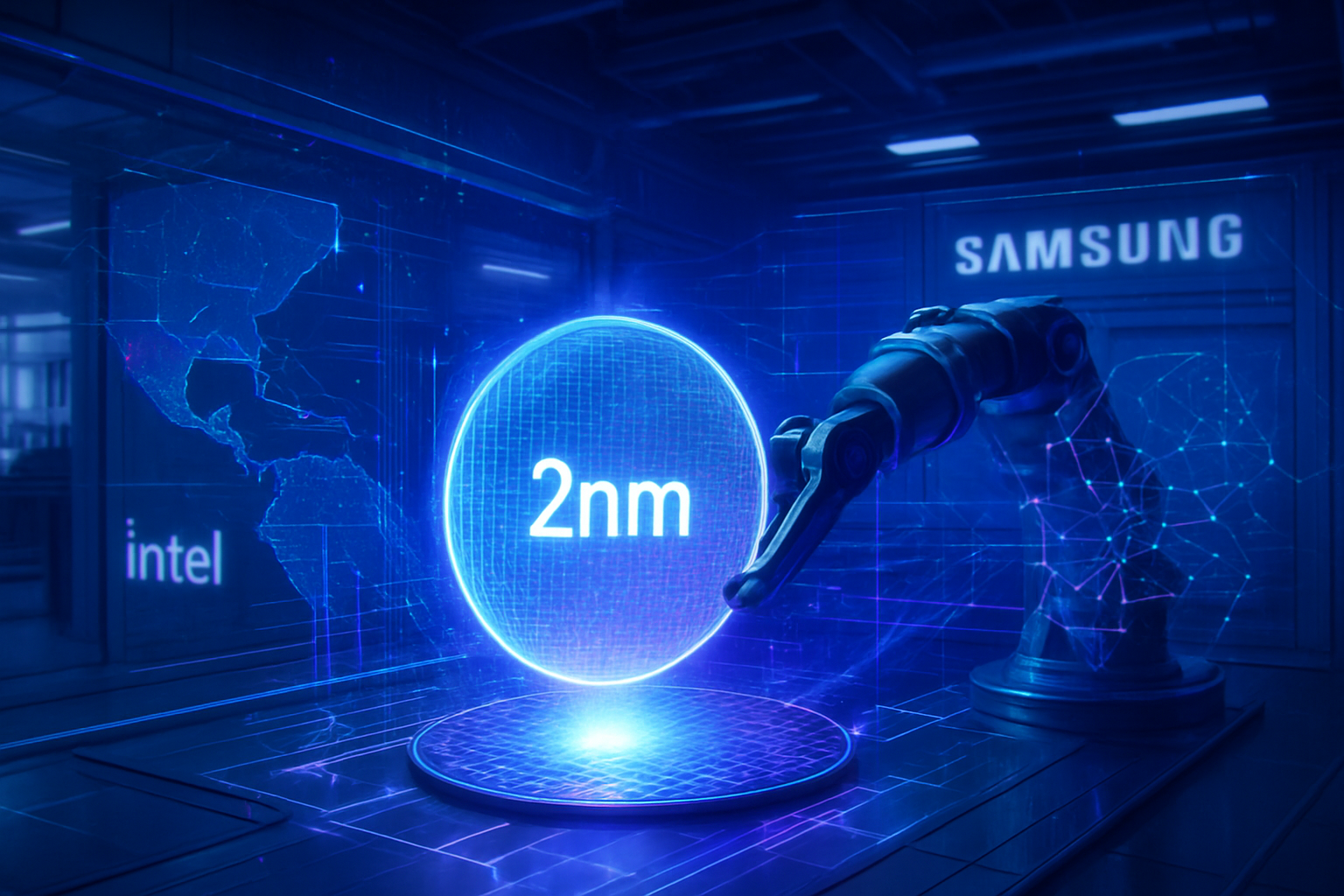
The specific technical focus of this delay centers on "legacy" or mature-node semiconductors. Unlike the cutting-edge 2nm and 3nm chips used in high-end AI servers and smartphones, legacy chips—typically defined as 28nm and older—are the workhorses of the modern economy. They power everything from power management systems in electric vehicles to industrial sensors and medical devices. By keeping the tariff rate at 0% until June 23, 2027, the US Department of Commerce is acknowledging that domestic alternatives and "friend-shoring" capacity in regions like India and Southeast Asia are not yet robust enough to absorb a total shift away from Chinese foundries like Semiconductor Manufacturing International Corp (HKG:0981).
This "calibrated" approach differs significantly from previous blanket tariff strategies. Instead of an immediate wall, the US is creating a "glide path." Industry experts suggest this gives companies like Intel Corporation (NASDAQ:INTC) and GlobalFoundries (NASDAQ:GFS) time to spin up their own mature-node capacity under the subsidies of the CHIPS Act. Initial reactions from the AI research and hardware communities have been cautiously optimistic, with analysts noting that an immediate 50% tariff would have likely crippled the mid-tier robotics and IoT sectors, which are currently undergoing an AI-driven transformation.
However, the technical specifications of this trade policy are rigid. The 0% window is strictly for legacy nodes; advanced AI hardware remains under heavy restriction. This distinction forces a bifurcated design philosophy: hardware designers must now choose between "Western-compliant" advanced stacks and "Legacy-compatible" systems that may still utilize Chinese components for the next 18 months. This has led to a surge in demand for supply chain transparency tools as firms scramble to audit every transistor's origin before the 2027 "cliff."
Market Impact: Tech Giants and the Race for Diversification
The market implications of this delay are profound, particularly for the "Magnificent Seven" and major semiconductor players. NVIDIA Corporation (NASDAQ:NVDA) and Apple Inc. (NASDAQ:AAPL), while focused on the leading edge, rely on a vast ecosystem of legacy components for their peripheral hardware. The 2027 delay prevents a sudden spike in Bill of Materials (BOM) costs, allowing these giants to maintain their aggressive R&D cycles. Conversely, Micron Technology, Inc. (NASDAQ:MU) and Texas Instruments (NASDAQ:TXN) are expected to accelerate their domestic expansion to capture the market share that will inevitably be vacated by Chinese firms when the tariffs eventually land.
The competitive landscape is also shifting toward new regional hubs. Taiwan Semiconductor Manufacturing Co. (NYSE:TSM) has seen its Kumamoto plant in Japan become a focal point of this diversification, with reports suggesting the facility may be upgraded to 2nm production sooner than expected to meet the demands of the "Silicon Nationalism" movement. In India, the Tata Group (NYSE:TTM) has become a primary beneficiary of Western capital, as its Dholera fab project is now viewed as a vital alternative for the 28nm-110nm chips that the US is currently sourcing from China.
Startups in the AI and robotics space are perhaps the most relieved by the 2027 extension. Many smaller firms lack the capital to re-engineer their products overnight. This window allows them to transition to "trusted" foundries without facing the existential threat of a 50% cost increase on their core components. However, the strategic advantage has clearly shifted to companies that can demonstrate a "China-free" supply chain early, as venture capital increasingly flows toward firms that are insulated from geopolitical volatility.
Silicon Nationalism: A New Global Order
This development is more than a trade dispute; it is the formalization of "Silicon Nationalism." This ideology posits that the ability to manufacture semiconductors is a sovereign right and a national security prerequisite. The recent formation of the "Pax Silica" alliance—a US-led bloc including Japan, South Korea, the UK, and the UAE—underscores this shift. This alliance aims to create a closed-loop ecosystem of "trusted" silicon, from the raw minerals to the final AI models, effectively creating a technological "Iron Curtain" that excludes adversarial nations.
The broader significance lies in how this mirrors previous industrial revolutions. Just as coal and oil defined 20th-century geopolitics, silicon and critical minerals like gallium are the 21st-century's strategic assets. China’s decision to weaponize its dominance in rare earth elements, even with the temporary "Busan Truce," serves as a stark reminder of the vulnerabilities inherent in the old globalized model. The US delay to 2027 is a recognition that building a parallel, secure supply chain is a multi-year endeavor that cannot be rushed without risking economic stability.
Critics and some industry veterans worry that this fragmentation will lead to "technological silos," where AI development in the West and East becomes increasingly incompatible. This could result in redundant R&D efforts and a slower overall pace of global innovation. However, proponents of Silicon Nationalism argue that the security benefits—preventing the use of foreign "backdoors" in critical infrastructure—far outweigh the costs of reduced efficiency.
The Road to 2027: Future Developments and Challenges
Looking ahead, the next 18 months will be a period of intense "foundry building." Experts predict a surge in construction for new fabs in Japan, India, and the US. Applied Materials, Inc. (NASDAQ:AMAT) and ASML Holding N.V. (NASDAQ:ASML) are expected to see record orders as nations race to equip their domestic facilities with the latest lithography and deposition tools. The challenge, however, remains the talent gap; building the physical plants is one thing, but training the thousands of specialized engineers required to run them is a hurdle that has yet to be fully cleared.
In the near term, watch for the "2026 Mineral Cliff." The current suspension of China’s export controls on gallium and germanium is set to expire in late 2026, just months before the US chip tariffs are scheduled to kick in. This could create a high-stakes "double whammy" for the tech industry if a new agreement is not reached. We can also expect to see the emergence of "AI-designed supply chains," where companies use advanced multi-agent AI systems to dynamically reroute their sourcing and logistics to stay ahead of shifting trade policies.
Conclusion: Navigating the New Silicon Frontier
The US decision to delay China chip tariffs to 2027 represents a rare moment of pragmatic restraint in an era of escalating tension. It acknowledges the deep interdependencies of the global tech sector while doubling down on the long-term goal of technological independence. The key takeaways are clear: the era of globalized, cost-first manufacturing is over, replaced by a security-first model that prioritizes resilience over price.
This shift will likely be remembered as a defining chapter in the history of the digital age—the moment when the "World Wide Web" began to fragment into localized "Sovereign Stacks." For investors and tech leaders, the coming months will require a delicate balancing act: leveraging the current 0% tariff window to maintain margins while aggressively investing in the "trusted" infrastructure of the future. The countdown to June 2027 has begun, and the race for silicon sovereignty is now the only game in town.
This content is intended for informational purposes only and represents analysis of current AI and semiconductor developments as of December 26, 2025.
TokenRing AI delivers enterprise-grade solutions for multi-agent AI workflow orchestration, AI-powered development tools, and seamless remote collaboration platforms.
For more information, visit https://www.tokenring.ai/.