As of December 22, 2025, the global semiconductor landscape has reached a definitive turning point. ASML Holding N.V. (NASDAQ: ASML), the linchpin of the world’s chipmaking supply chain, is now operating under the most stringent export regime in its history. Following a series of coordinated policy shifts between the United States and the Netherlands throughout late 2024 and 2025, the company has effectively seen its once-dominant market share in China restricted to a fraction of its former self, signaling a profound "normalization" of the industry’s geographic revenue mix.
This development marks the culmination of years of geopolitical tension, where Deep Ultraviolet (DUV) lithography—the workhorse technology used to manufacture everything from automotive chips to advanced AI processors—has become the primary battlefield. The immediate significance lies in the successful "harmonization" of export rules between Washington and The Hague, a move that has closed previous loopholes and forced ASML to pivot its long-term growth strategy toward South Korea and the United States, even as Chinese domestic firms scramble to find workarounds.
Technical Tightening: From EUV to DUV and Beyond
The core of the recent restrictions centers on ASML’s immersion DUV systems, specifically the TWINSCAN NXT:1970i and NXT:1980i. While these systems were once considered "mid-range" compared to the cutting-edge Extreme Ultraviolet (EUV) machines, their ability to produce 7nm-class chips through multi-patterning techniques made them a target for U.S. regulators. In a significant policy shift that took effect in late 2024, the Dutch government expanded its licensing requirements to include these specific DUV models, effectively taking over jurisdiction from the U.S. Foreign Direct Product Rule to create a unified Western front.
Beyond the hardware itself, the December 2024 U.S. "Advanced Computing and Semiconductor Manufacturing Equipment Rule" introduced granular controls on metrology and software. These rules prevent ASML from providing high-level system upgrades that could improve "overlay accuracy"—the precision with which layers of a chip are aligned—by more than 1%. This technical ceiling is designed to prevent Chinese fabs from squeezing more performance out of existing equipment. Industry experts note that while ASML can still provide basic maintenance, the prohibition on performance-enhancing software updates represents a "soft-kill" of the machines' long-term competitiveness for advanced nodes.
Market Realignment: The Rise of South Korea and the China Pivot
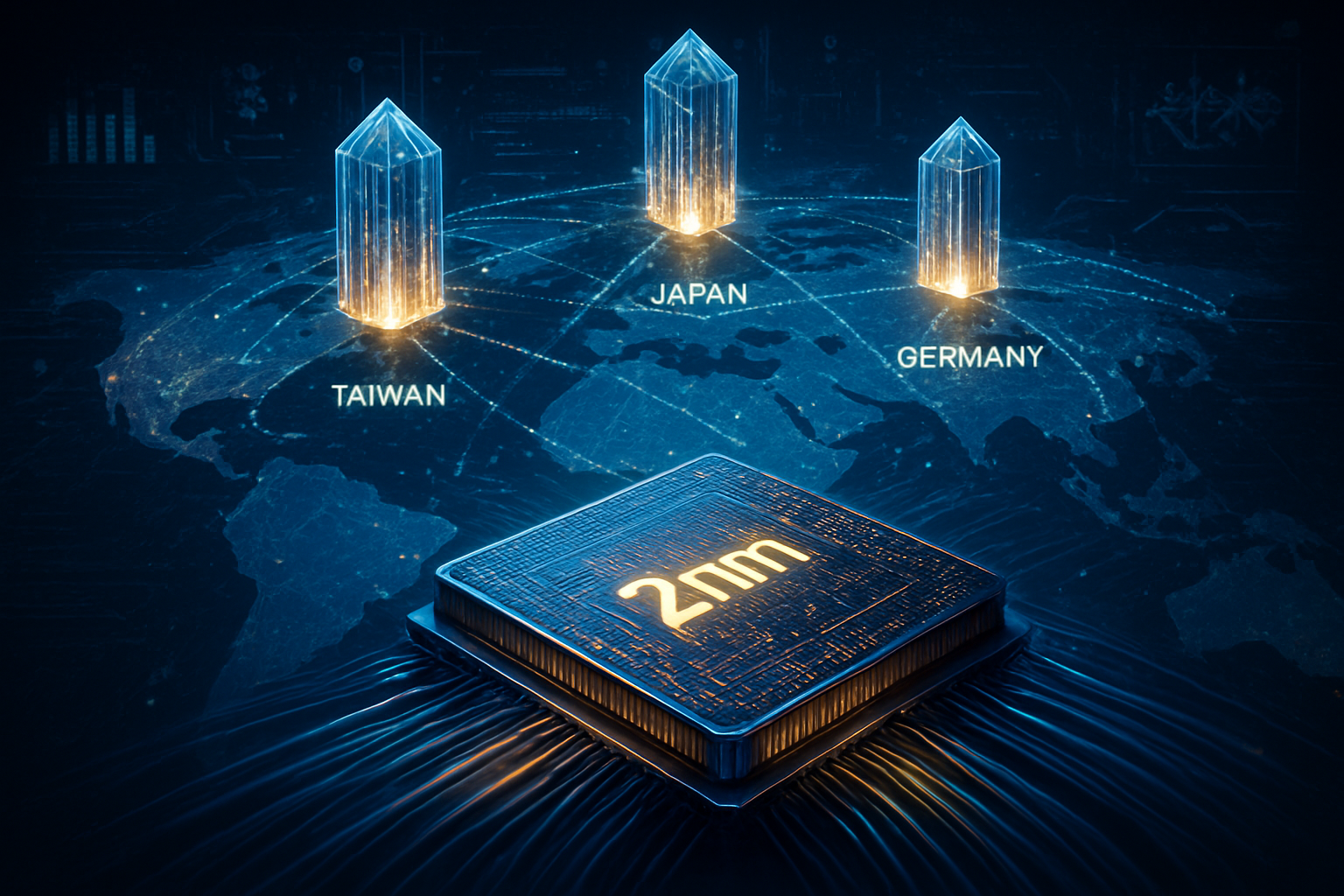
The financial impact of these rules has been stark but, according to ASML leadership, "entirely expected." In 2024, China accounted for a staggering 49% of ASML’s revenue as Chinese firms engaged in a massive stockpiling effort. By the end of 2025, that figure has plummeted to approximately 20%. ASML’s total net sales guidance remains robust at €30 billion to €35 billion, but the source of that capital has shifted. South Korea has emerged as the company’s largest market, accounting for 40% of system sales in 2025, driven by massive investments from memory giants and AI-focused foundries.
For major players like Taiwan Semiconductor Manufacturing Company (NYSE: TSM) and Intel Corporation (NASDAQ: INTC), the restriction on China provides a competitive breather, ensuring that the most advanced lithography tools remain concentrated in allied nations. However, the loss of high-margin DUV sales to China has had a dilutive effect on ASML’s gross margin, which is currently hovering between 51% and 53%—slightly lower than the 55%+ margins seen during the China-driven boom of the early 2020s.
The Geopolitical Landscape: 'Pax Silica' and European Alignment
The year 2025 has seen the emergence of a new geopolitical framework known as "Pax Silica." This U.S.-led strategic alliance, which includes the Netherlands, Japan, South Korea, and the UK, aims to secure the AI and semiconductor supply chain against external shocks and technological leakage. The Netherlands’ decision to join this initiative in December 2025 marks a final departure from its previous "cautious cooperation" stance, fully aligning Dutch economic security with U.S. interests.
This alignment is mirrored in the broader European Union’s updated Economic Security Strategy. While the EU maintains a "country-agnostic" rhetoric, the practical application of its policies has clearly targeted reducing dependencies on high-risk regions for critical technologies. This shift has raised concerns among some European trade advocates who fear the loss of the Chinese market will lead to a "dual-track" global economy, where China develops its own, albeit less efficient, domestic lithography ecosystem, potentially led by state-backed firms like Shanghai Micro Electronics Equipment (SMEE).
Future Outlook: The 7nm Battle and AI Demand
Looking ahead to 2026, the primary challenge for the export control regime will be the "secondary market" and indigenous Chinese innovation. Despite the restrictions, firms like Huawei and SMIC (HKG: 0981) have successfully utilized older DUV kits and third-party engineering to maintain 7nm production. Experts predict that the next phase of restrictions will likely focus on the spare parts market and the movement of specialized personnel, as the U.S. and its allies seek to degrade China's existing installed base of lithography tools.
In the near term, the explosion in AI demand is expected to more than offset the revenue lost from China. The rollout of ASML’s High-NA (Numerical Aperture) EUV systems is accelerating, with major logic and memory customers in the U.S. and Asia ramping up capacity for the next generation of 2nm and 1.4nm chips. The challenge for ASML will be managing the complex logistics of a supply chain that is increasingly fragmented by national security concerns while maintaining the rapid pace of innovation required by the AI revolution.
A New Status Quo in Silicon Diplomacy
The events of late 2025 have solidified a new status quo for the semiconductor industry. ASML has successfully navigated a geopolitical minefield, maintaining its financial health and technological leadership despite the loss of its largest growth engine in China. The "normalization" of the China market share to 20% represents a successful, if painful, decoupling that has fundamentally altered the company’s geographic footprint.
As we move into 2026, the industry will be watching for two key signals: the effectiveness of Chinese domestic lithography breakthroughs and the potential for even stricter controls on "legacy" nodes (28nm and above). For now, ASML remains the indispensable architect of the digital age, but it is an architect that must now build its future within the increasingly rigid walls of a bifurcated global trade system.
This content is intended for informational purposes only and represents analysis of current AI and semiconductor developments.
TokenRing AI delivers enterprise-grade solutions for multi-agent AI workflow orchestration, AI-powered development tools, and seamless remote collaboration platforms.
For more information, visit https://www.tokenring.ai/.