CHANDLER, AZ – In a move that marks the most significant architectural shift in semiconductor manufacturing in over a decade, the industry has officially transitioned into what experts are calling the "Glass Age." As of January 21, 2026, the transition from traditional organic substrates to glass-core technology, coupled with the arrival of the first circuit-ready 3D Complementary Field-Effect Transistors (CFET), has effectively dismantled the physical barriers that threatened to stall the progress of generative AI.
This development is not merely an incremental upgrade; it is a foundational reset. By replacing the resin-based materials that have housed chips for forty years with ultra-flat, thermally stable glass, manufacturers are now able to build "super-packages" of unprecedented scale. These advancements arrive just in time to power the next generation of trillion-parameter AI models, which have outgrown the electrical and thermal limits of 2024-era hardware.
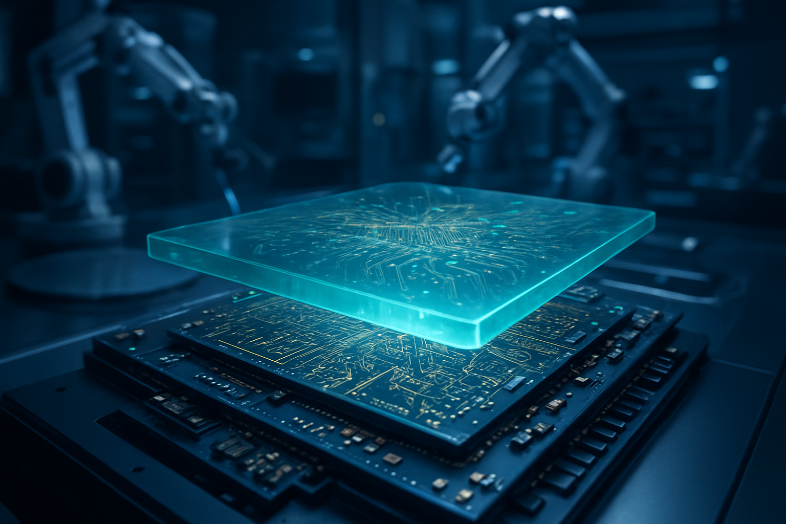
Shattering the "Warpage Wall": The Tech Behind the Transition
The technical shift centers on the transition from Ajinomoto Build-up Film (ABF) organic substrates to glass-core substrates. For years, the industry struggled with the "warpage wall"—a phenomenon where the heat generated by massive AI chips caused traditional organic substrates to expand and contract at different rates than the silicon they supported, leading to microscopic cracks and connection failures. Glass, by contrast, possesses a Coefficient of Thermal Expansion (CTE) that nearly matches silicon. This allows companies like Intel (NASDAQ: INTC) and Samsung (OTC: SSNLF) to manufacture packages exceeding 100mm x 100mm, integrating dozens of chiplets and HBM4 (High Bandwidth Memory) stacks into a single, cohesive unit.
Beyond the substrate, the industry has reached a milestone in transistor architecture with the successful demonstration of the first fully functional 101-stage monolithic CFET Ring Oscillator by TSMC (NYSE: TSM). While the previous Gate-All-Around (GAA) nanosheets allowed for greater control over current, CFET takes scaling into the third dimension by vertically stacking n-type and p-type transistors directly on top of one another. This 3D stacking effectively halves the footprint of logic gates, allowing for a 10x increase in interconnect density through the use of Through-Glass Vias (TGVs). These TGVs enable microscopic electrical paths with pitches of less than 10μm, reducing signal loss by 40% compared to traditional organic routing.
The New Hierarchy: Intel, Samsung, and the Race for HVM
The competitive landscape of the semiconductor industry has been radically reordered by this transition. Intel (NASDAQ: INTC) has seized an early lead, announcing this month that its facility in Chandler, Arizona, has officially moved glass substrate technology into High-Volume Manufacturing (HVM). Its first commercial product utilizing this technology, the Xeon 6+ "Clearwater Forest," is already shipping to major cloud providers. Intel’s early move positions its Foundry Services as a critical partner for US-based AI giants like Amazon (NASDAQ: AMZN) and Google (NASDAQ: GOOGL), who are seeking to insulate their supply chains from geopolitical volatility.
Samsung (KRX: 005930), meanwhile, has leveraged its "Triple Alliance"—a collaboration between its Foundry, Display, and Electro-Mechanics divisions—to fast-track its "Dream Substrate" program. Samsung is targeting the second half of 2026 for mass production, specifically aiming for the high-end AI ASIC market. Not to be outdone, TSMC (NYSE: TSM) has begun sampling its Chip-on-Panel-on-Substrate (CoPoS) glass solution for Nvidia (NASDAQ: NVDA). Nvidia’s newly announced "Vera Rubin" R100 platform is expected to be the primary beneficiary of this tech, aiming for a 5x boost in AI inference capabilities by utilizing the superior signal integrity of glass to manage its staggering 19.6 TB/s HBM4 bandwidth.
Geopolitics and Sustainability: The High Stakes of High Tech
The shift to glass has created a new geopolitical "moat" around the Western-Korean semiconductor axis. As the manufacturing of these advanced substrates requires high-precision equipment and specialized raw materials—such as the low-CTE glass cloth produced almost exclusively by Japan’s Nitto Boseki—a new bottleneck has emerged. US and South Korean firms have secured long-term contracts for these materials, creating a 12-to-18-month lead over Chinese rivals like BOE and Visionox, who are currently struggling with high-volume yields. This technological gap has become a cornerstone of the US strategy to maintain leadership in high-performance computing (HPC).
From a sustainability perspective, the move is a double-edged sword. The manufacturing of glass substrates is more energy-intensive than organic ones, requiring high-temperature furnaces and complex water-reclamation protocols. However, the operational benefits are transformative. By reducing power loss during data movement by 50%, glass-packaged chips are significantly more energy-efficient once deployed in data centers. In an era where AI power consumption is measured in gigawatts, the "Performance per Watt" advantage of glass is increasingly seen as the only viable path to sustainable AI scaling.
Future Horizons: From Electrical to Optical
Looking toward 2027 and beyond, the transition to glass substrates paves the way for the "holy grail" of chip design: integrated co-packaged optics (CPO). Because glass is transparent and ultra-flat, it serves as a perfect medium for routing light instead of electricity. Experts predict that within the next 24 months, we will see the first AI chips that use optical interconnects directly on the glass substrate, virtually eliminating the "power wall" that currently limits how fast data can move between the processor and memory.
However, challenges remain. The brittleness of glass continues to pose yield risks, with current manufacturing lines reporting breakage rates roughly 5-10% higher than organic counterparts. Additionally, the industry must develop new standardized testing protocols for 3D-stacked CFET architectures, as traditional "probing" methods are difficult to apply to vertically stacked transistors. Industry consortiums are currently working to harmonize these standards to ensure that the "Glass Age" doesn't suffer from a lack of interoperability.
A Decisive Moment in AI History
The transition to glass substrates and 3D transistors marks a definitive moment in the history of computing. By moving beyond the physical limitations of 20th-century materials, the semiconductor industry has provided AI developers with the "infinite" canvas required to build the first truly agentic, world-scale AI systems. The ability to stitch together dozens of chiplets into a single, thermally stable package means that the 1,000-watt AI accelerator is no longer a thermal nightmare, but a manageable reality.
As we move into the spring of 2026, all eyes will be on the yield rates of Intel's Arizona lines and the first performance benchmarks of AMD’s (NASDAQ: AMD) Instinct MI400 series, which is slated to utilize glass substrates from merchant supplier Absolics later this year. The "Silicon Valley" of the future may very well be built on a foundation of glass, and the companies that master this transition first will likely dictate the pace of AI innovation for the remainder of the decade.
This content is intended for informational purposes only and represents analysis of current AI developments.
TokenRing AI delivers enterprise-grade solutions for multi-agent AI workflow orchestration, AI-powered development tools, and seamless remote collaboration platforms.
For more information, visit https://www.tokenring.ai/.