Tag: Global Supply Chain

  • India’s Silicon Revolution: Groundbreaking for Dholera Fab Marks Bold Leap Toward 2032 Semiconductor Leadership

    India’s Silicon Revolution: Groundbreaking for Dholera Fab Marks Bold Leap Toward 2032 Semiconductor Leadership

    The landscape of global electronics manufacturing shifted significantly this week as India officially commenced the next phase of its ambitious semiconductor journey. The groundbreaking for the country’s first commercial semiconductor fabrication facility (fab) in the Dholera Special Investment Region (SIR) of Gujarat represents more than just a construction project; it is the physical manifestation of India’s intent to become a premier global tech hub. Spearheaded by a strategic partnership between Tata Electronics and Taiwan’s Powerchip Semiconductor Manufacturing Corp. (TWSE: 6770), the $11 billion (₹91,000 crore) facility is the cornerstone of the India Semiconductor Mission (ISM), aiming to insulate the nation from global supply chain shocks while fueling domestic high-tech growth.

    This milestone comes at a critical juncture as the Indian government doubles down on its long-term vision. Union ministers have reaffirmed a target for India to rank among the top four semiconductor nations globally by 2032, with an even more aggressive goal to lead the world in specific semiconductor verticals by 2035. For a nation that has historically excelled in chip design but lagged in physical manufacturing, the Dholera fab serves as the "anchor tenant" for a massive "Semicon City" ecosystem, signaling to the world that India is no longer just a consumer of technology, but a primary architect and manufacturer of it.

    Technical Specifications and Industry Impact

    The Dholera fab is engineered to be a high-volume, state-of-the-art facility capable of producing 50,000 12-inch wafers per month at full capacity. Technically, the facility is focusing its initial efforts on the 28-nanometer (nm) technology node. While advanced logic chips for smartphones often utilize smaller nodes like 3nm or 5nm, the 28nm node remains the "sweet spot" for a vast array of high-demand applications. These include Power Management Integrated Circuits (PMICs), display drivers, and microcontrollers essential for the automotive and industrial sectors. The facility is also designed with the flexibility to support mature nodes ranging from 40nm to 110nm, ensuring a wide-reaching impact on the electronics ecosystem.

    Initial reactions from the global semiconductor research community have been overwhelmingly positive, particularly regarding the partnership with PSMC. By leveraging the Taiwanese firm’s deep expertise in logic and memory manufacturing, Tata Electronics is bypassing decades of trial-and-error. Technical experts have noted that the "AI-integrated" infrastructure of the fab—which includes advanced automation and real-time data analytics for yield optimization—differentiates this project from traditional fabs in the region. The recent arrival of specialized lithography and etching equipment from Tokyo Electron (TYO: 8035) and other global leaders underscores the facility's readiness to meet international precision standards.

    Strategic Advantages for Tech Giants and Startups

    The establishment of this fab creates a seismic shift for major players across the tech spectrum. The primary beneficiary within the domestic market is the Tata Group, which can now integrate its own chips into products from Tata Motors Limited (NSE: TATAMOTORS) and its aerospace ventures. This vertical integration provides a massive strategic advantage in cost control and supply security. Furthermore, global tech giants like Micron Technology (NASDAQ: MU), which is already operating an assembly and test plant in nearby Sanand, now have a domestic wafer source, potentially reducing the lead times and logistics costs that have historically plagued the Indian electronics market.

    Competitive implications are also emerging for major AI labs and hardware companies. As the Dholera fab scales, it will likely disrupt the existing dominance of East Asian manufacturing hubs. By offering a "China Plus One" alternative, India is positioning itself as a reliable secondary source for global giants like Apple and NVIDIA (NASDAQ: NVDA), who are increasingly looking to diversify their manufacturing footprints. Startups in India’s burgeoning EV and IoT sectors are also expected to see a surge in innovation, as they gain access to localized prototyping and a more responsive supply chain that was previously tethered to overseas lead times.

    Broader Significance in the Global Landscape

    Beyond the immediate commercial impact, the Dholera project carries profound geopolitical weight. In the broader AI and technology landscape, semiconductors have become the new "oil," and India’s entry into the fab space is a calculated move to secure technological sovereignty. This development mirrors the significant historical milestones of the 1980s when Taiwan and South Korea first entered the market; if successful, India’s 2032 goal would mark one of the fastest ascents of a nation into the semiconductor elite in history.

    However, the path is not without its hurdles. Concerns have been raised regarding the massive requirements for ultrapure water and stable high-voltage power, though the Gujarat government has fast-tracked a dedicated 1.5-gigawatt power grid and specialized water treatment facilities to address these needs. Comparisons to previous failed attempts at Indian semiconductor manufacturing are inevitable, but the difference today lies in the unprecedented level of government subsidies—covering up to 50% of project costs—and the deep involvement of established industrial conglomerates like Tata Steel Limited (NSE: TATASTEEL) to provide the foundational infrastructure.

    Future Horizons and Challenges

    Looking ahead, the roadmap for India’s semiconductor mission is both rapid and expansive. Following the stabilization of the 28nm node, the Tata-PSMC joint venture has already hinted at plans to transition to 22nm and eventually explore smaller logic nodes by the turn of the decade. Experts predict that as the Dholera ecosystem matures, it will attract a cluster of "OSAT" (Outsourced Semiconductor Assembly and Test) and ATMP (Assembly, Testing, Marking, and Packaging) facilities, creating a fully integrated value chain on Indian soil.

    The near-term focus will be on "tool-in" milestones and pilot production runs, which are expected to commence by late 2026. One of the most significant challenges on the horizon will be talent cultivation; to meet the goal of being a top-four nation, India must train hundreds of thousands of specialized engineers. Programs like the "Chips to Startup" (C2S) initiative are already underway to ensure that by the time the Dholera fab reaches peak capacity, there is a workforce ready to operate and innovate within its walls.

    A New Era for Indian Silicon

    In summary, the groundbreaking at Dholera is a watershed moment for the Indian economy and the global technology supply chain. By partnering with PSMC and committing billions in capital, India is transitioning from a service-oriented economy to a high-tech manufacturing powerhouse. The key takeaways are clear: the nation has a viable path to 28nm production, a massive captive market through the Tata ecosystem, and a clear, state-backed mandate to dominate the global semiconductor stage by 2032.

    As we move through 2026, all eyes will be on the construction speed and the integration of supply chain partners like Applied Materials (NASDAQ: AMAT) and Lam Research (NASDAQ: LRCX) into the Dholera SIR. The success of this fab will not just be measured in wafers produced, but in the shift of the global technological balance of power. For the first time, "Made in India" chips are no longer a dream of the future, but a looming reality for the global market.


    This content is intended for informational purposes only and represents analysis of current AI and semiconductor developments.

    TokenRing AI delivers enterprise-grade solutions for multi-agent AI workflow orchestration, AI-powered development tools, and seamless remote collaboration platforms.
    For more information, visit https://www.tokenring.ai/.

  • Silicon Sovereignty: India’s Semiconductor Revolution Hits Commercial Milestone in 2026

    Silicon Sovereignty: India’s Semiconductor Revolution Hits Commercial Milestone in 2026

    As of January 2, 2026, the global technology landscape is witnessing a historic shift as India officially transitions from a software powerhouse to a hardware heavyweight. This month marks the commencement of high-volume commercial production at several key semiconductor facilities across the country, signaling the realization of India’s ambitious "Silicon Shield" strategy. With the India Semiconductor Mission (ISM) successfully anchoring over $18 billion in cumulative investments, the nation is no longer just a design hub for global giants; it is now a critical manufacturing node in the global supply chain.

    The arrival of 2026 has brought the much-anticipated "ramp-up" phase for industry leaders. Micron Technology (NASDAQ: MU) has begun high-volume commercial exports of DRAM and NAND memory products from its Sanand, Gujarat facility, while Kaynes Technology India (NSE: KAYNES) has officially entered full-scale production this week. These milestones represent a definitive break from decades of import dependency, positioning India as a resilient alternative in a world increasingly wary of geopolitical volatility in the Taiwan Strait and East Asia.

    From Blueprints to Silicon: Technical Milestones of 2026

    The technical landscape of India’s semiconductor rise is characterized by a strategic focus on "workhorse" mature nodes and advanced packaging. At the heart of this revolution is the Tata Electronics mega-fab in Dholera, a joint venture with Powerchip Semiconductor Manufacturing Corp (TWSE: 6770). While the fab is currently in the intensive equipment installation phase, it is on track to roll out India’s first indigenously manufactured 28nm to 110nm chips by December 2026. These nodes are essential for the automotive, telecommunications, and power electronics sectors, which form the backbone of the modern industrial economy.

    In the Assembly, Test, Marking, and Packaging (ATMP) segment, the progress is even more immediate. Micron Technology’s Sanand plant has validated its 500,000-square-foot cleanroom space and is now processing advanced memory modules for global distribution. Similarly, Kaynes Semicon achieved a technical breakthrough in late 2025 by shipping India’s first commercially manufactured Multi-Chip Modules (MCM) to Alpha & Omega Semiconductor (NASDAQ: AOS). This capability to package complex power semiconductors locally is a significant departure from previous years, where Indian firms were limited to circuit board assembly.

    Initial reactions from the global semiconductor community have been overwhelmingly positive. Experts at the 2025 SEMICON India summit noted that the speed of construction in the Dholera and Sanand clusters has rivaled that of traditional hubs like Hsinchu or Arizona. By focusing on 28nm and 40nm nodes, India has avoided the "bleeding edge" risks of sub-5nm logic, instead capturing the high-demand "foundational" chip market that caused the most severe supply chain bottlenecks during the early 2020s.

    Corporate Maneuvers and the "China Plus One" Strategy

    The commercialization of Indian chips is fundamentally altering the strategic calculus for tech giants and startups alike. For companies like Renesas Electronics (TYO: 6723), which partnered with CG Power and Industrial Solutions (NSE: CGPOWER), the Indian venture provides a vital de-risking mechanism. Their joint OSAT facility in Sanand, which began pilot runs in late 2025, is now transitioning to commercial production of chips for the 5G and electric vehicle (EV) sectors. This move has allowed Renesas to diversify its manufacturing base away from concentrated clusters in East Asia, a strategy now widely termed "China Plus One."

    Major AI and consumer electronics firms stand to benefit significantly from this localization. With Foxconn (TWSE: 2317) and HCL Technologies (NSE: HCLTECH) receiving approval for their own OSAT facility in Uttar Pradesh in mid-2025, the synergy between chip manufacturing and device assembly is reaching a tipping point. Analysts predict that by late 2026, the "Made in India" iPhone or Samsung device will not just be assembled in the country but will also contain memory and power management chips fabricated or packaged within Indian borders.

    However, the journey has not been without its corporate casualties. The high-profile $11 billion fab proposal by the Adani Group and Tower Semiconductor (NASDAQ: TSEM) remains in a state of strategic pause as of January 2026, failing to secure the necessary central subsidies due to disagreements over financial commitments. Similarly, the entry of software giant Zoho into the fab space was shelved in early 2025. These developments highlight the brutal capital intensity and technical rigor required to succeed in the semiconductor arena, where only the most committed players survive.

    Geopolitics and the Quest for Tech Sovereignty

    Beyond the corporate balance sheets, India’s semiconductor rise is a cornerstone of its "Tech Sovereignty" doctrine. In a world where technology and trade are increasingly weaponized, the ability to manufacture silicon is equivalent to national security. Union Minister Ashwini Vaishnaw recently remarked that the "Silicon Shield" is now extending to the Indian subcontinent, providing a layer of protection against global supply shocks. This sentiment is echoed by the Indian government’s commitment to "ISM 2.0," a second phase of the mission focusing on localizing the supply of specialty chemicals, gases, and substrates.

    This shift has profound implications for the global AI landscape. As AI workloads migrate to the edge—into cars, appliances, and industrial robots—the demand for mature-node chips and advanced packaging (like the Integrated Systems Packaging at Tata’s Assam plant) is skyrocketing. India’s entry into this market provides a much-needed pressure valve for the global supply chain, which has remained precariously dependent on a few square miles of territory in Taiwan.

    Potential concerns remain, particularly regarding the environmental impact of large-scale fabrication and the immense water requirements of the Dholera cluster. However, the Indian government has countered these fears by mandating "Green Fab" standards, utilizing recycled water and solar power for the new facilities. Compared to previous industrial milestones like the software revolution of the 1990s, the semiconductor rise of 2026 is a far more capital-intensive and physically tangible transformation of the Indian economy.

    The Horizon: ISM 2.0 and the Talent Pipeline

    Looking toward the near-term future, the focus is shifting from building factories to building a comprehensive ecosystem. By early 2026, India has already trained over 60,000 semiconductor engineers toward its goal of 85,000, effectively mitigating the talent shortages that have plagued fab projects in the United States and Europe. The next 12 to 24 months will likely see a surge in "Design-Linked Incentive" (DLI) startups, as Indian engineers move from designing chips for Western firms to creating indigenous IP for the global market.

    On the horizon, we expect to see the first commercial production of Silicon Carbide (SiC) wafers in Odisha by RIR Power Electronics by March 2026. This will be a game-changer for the EV industry, as SiC chips are significantly more efficient than traditional silicon for high-voltage applications. Challenges remain in the "chemical localization" space, but experts predict that the presence of anchor tenants like Micron and Tata will naturally pull the entire supply chain—including equipment manufacturers and raw material suppliers—into the Indian orbit by 2027.

    A New Era for the Global Chip Industry

    The events of January 2026 mark a definitive "before and after" moment in India's industrial history. The transition from pilot lines to commercial shipping manifests a level of execution that many skeptics doubted only three years ago. India has successfully navigated the "valley of death" between policy announcement and hardware production, proving that it can provide a stable, high-tech alternative to traditional manufacturing hubs.

    As we look forward, the key to watch will be the "yield rates" of the Tata-PSMC fab and the successful scaling of the Assam ATMP facility. If these projects hit their targets by the end of 2026, India will firmly establish itself as the fourth pillar of the global semiconductor industry, alongside the US, Taiwan, and South Korea. For the tech world, the message is clear: the future of silicon is no longer just in the East or the West—it is increasingly in the heart of the Indian subcontinent.


    This content is intended for informational purposes only and represents analysis of current AI and semiconductor developments.

    TokenRing AI delivers enterprise-grade solutions for multi-agent AI workflow orchestration, AI-powered development tools, and seamless remote collaboration platforms.
    For more information, visit https://www.tokenring.ai/.

  • The Silicon Silk Road: India and the Netherlands Forge a New Semiconductor Axis for the AI Era

    The Silicon Silk Road: India and the Netherlands Forge a New Semiconductor Axis for the AI Era

    In a move that signals a tectonic shift in the global technology landscape, India and the Netherlands have today, December 19, 2025, finalized the "Silicon Silk Road" strategic alliance. This comprehensive framework, signed in New Delhi, aims to bridge the gap between European high-tech precision and Indian industrial scale. By integrating the Netherlands’ world-leading expertise in lithography and semiconductor equipment with India’s rapidly expanding manufacturing ecosystem, the partnership seeks to create a resilient, alternative supply chain for the high-performance hardware required to power the next generation of artificial intelligence.

    The immediate significance of this alliance cannot be overstated. As the global demand for AI-optimized chips—specifically those capable of handling massive large language model (LLM) training and edge computing—reaches a fever pitch, the "Silicon Silk Road" provides a blueprint for a decentralized manufacturing future. The agreement moves beyond simple trade, establishing a co-development model that includes technology transfers, joint R&D in advanced materials, and the creation of specialized maintenance hubs that will ensure India’s upcoming fabrication units (fabs) operate with the world’s most advanced Dutch-made machinery.

    Technical Foundations: Lithography, Labs, and Lab-Grown Diamonds

    The core of the alliance is built upon unprecedented commitments from Dutch semiconductor giants. NXP Semiconductors N.V. (NASDAQ:NXPI) has officially announced a massive $1 billion investment to double its research and development presence in India. This expansion is focused on the design of 5-nanometer automotive and AI chips, with a new R&D center slated for the Greater Noida Semiconductor Park. Unlike previous design-only centers, this facility will work in tandem with Indian manufacturing partners to prototype "system-on-chip" (SoC) architectures specifically optimized for low-latency AI applications.

    Simultaneously, ASML Holding N.V. (NASDAQ:ASML) is shifting its strategy from a vendor-client relationship to a deep-tier partnership. For the first time, ASML will establish "Holistic Lithography" maintenance labs within India. These labs are designed to provide real-time technical support and software calibration for the Extreme Ultraviolet (EUV) and Deep Ultraviolet (DUV) lithography systems that are essential for high-end chip production. This differs from existing models where technical expertise was centralized in Europe or East Asia, effectively removing a significant bottleneck for Indian fab operators like the Tata Group and Micron Technology, Inc. (NASDAQ:MU).

    One of the most technically ambitious aspects of the 2025 framework is the joint research into lab-grown diamonds (LGD) as a substrate for semiconductors. Leveraging India’s established diamond-processing hub in Surat and Dutch precision engineering, the partnership aims to develop diamond-based chips that can handle significantly higher thermal loads than traditional silicon. This breakthrough could revolutionize AI hardware, where heat management is currently a primary limiting factor for processing density in data centers.

    Strategic Realignment: Winners in the New Hardware Race

    The "Silicon Silk Road" creates a new competitive theater for the world’s largest AI labs and hardware providers. Companies like NVIDIA Corporation (NASDAQ:NVDA) and Advanced Micro Devices, Inc. (NASDAQ:AMD) stand to benefit immensely from a more diversified manufacturing base. By having a viable, Dutch-supported manufacturing alternative in India, these tech giants can mitigate the geopolitical risks associated with the current concentration of production in East Asia. The alliance provides a "China+1" strategy with teeth, offering a stable environment backed by European intellectual property protections and Indian production-linked incentives (PLI).

    For the Netherlands, the alliance secures a massive, long-term market for its high-tech exports at a time when global trade restrictions are tightening. ASML and NXP are effectively "future-proofing" their revenue streams by embedding themselves into the foundation of India’s digital infrastructure. Meanwhile, Indian tech conglomerates and startups are gaining access to the "holy grail" of semiconductor manufacturing: the ability to move from chip design to domestic fabrication with the support of the world’s most advanced equipment manufacturers. This positioning gives Indian firms a strategic advantage in the burgeoning field of "Sovereign AI," where nations seek to control their own computational resources.

    Geopolitics and the Global AI Landscape

    The emergence of the Silicon Silk Road fits into a broader trend of "techno-nationalism," where semiconductor self-sufficiency is viewed as a pillar of national security. This partnership is a direct response to the fragility of global supply chains exposed during the early 2020s. By forging this link, India and the Netherlands are creating a middle path that avoids the binary choice between US-led and China-led ecosystems. It is a milestone comparable to the early 2000s outsourcing boom, but with a critical difference: this time, India is moving up the value chain into the most complex manufacturing process ever devised by humanity.

    However, the alliance does not come without concerns. Industry analysts have pointed to the immense energy requirements of advanced fabs and the potential environmental impact of large-scale semiconductor manufacturing in India. Furthermore, the transfer of highly sensitive lithography technology requires a level of cybersecurity and intellectual property protection that will be a constant test for Indian regulators. Comparing this to previous milestones like the CHIPS Act, the Silicon Silk Road is unique because it relies on bilateral synergy rather than unilateral subsidies, blending Dutch technical precision with India’s demographic dividend.

    The Horizon: 2026 and Beyond

    Looking ahead, the next 24 months will be critical for the execution of the 2025 framework. The immediate goal is the operationalization of the first joint R&D labs and the commencement of training for the first cohort of 85,000 semiconductor professionals that India aims to produce by 2030. Near-term developments will likely include the announcement of a joint venture between an Indian industrial house and a Dutch equipment firm to manufacture semiconductor components—not just chips—locally, further deepening the supply chain.

    The long-term vision involves the commercialization of the lab-grown diamond substrate technology, which could place the India-Netherlands axis at the forefront of "Beyond Silicon" computing. Experts predict that by 2028, the first AI accelerators featuring "Made in India" chips, fabricated using ASML-supported systems, will hit the global market. The primary challenge will be maintaining the pace of infrastructure development—specifically stable power and ultra-pure water supplies—to match the requirements of the high-tech machinery being deployed.

    Conclusion: A New Chapter in Industrial History

    The signing of the Silicon Silk Road alliance marks the end of an era where semiconductor manufacturing was the exclusive domain of a few select geographies. It represents a maturation of India’s industrial ambitions and a strategic pivot for the Netherlands as it seeks to maintain its technological edge in an increasingly fragmented world. The key takeaway is clear: the future of AI hardware will not be determined by a single nation, but by the strength and resilience of the networks they build.

    As we move into 2026, the global tech community will be watching the progress in Greater Noida and the research labs of Eindhoven with intense interest. The success of this partnership could serve as a model for other nations looking to secure their technological future. For now, the "Silicon Silk Road" stands as a testament to the power of strategic collaboration in the age of artificial intelligence, promising to reshape the hardware that will define the rest of the 21st century.


    This content is intended for informational purposes only and represents analysis of current AI developments.

    TokenRing AI delivers enterprise-grade solutions for multi-agent AI workflow orchestration, AI-powered development tools, and seamless remote collaboration platforms.
    For more information, visit https://www.tokenring.ai/.

  • Silicon Silk Road: India and the Netherlands Forge Strategic Alliance to Redefine Global Semiconductor Manufacturing

    Silicon Silk Road: India and the Netherlands Forge Strategic Alliance to Redefine Global Semiconductor Manufacturing

    In a move that signals a tectonic shift in the global technology landscape, India and the Netherlands have officially entered into a series of landmark agreements aimed at transforming India into a premier semiconductor powerhouse. Signed on December 19, 2025, during a high-level diplomatic visit to New Delhi, these Memoranda of Understanding (MoUs) establish a comprehensive framework for cooperation in advanced chip manufacturing, research and development, and digital security. The alliance effectively bridges the gap between Europe’s leading semiconductor equipment expertise and India’s rapidly scaling manufacturing ambitions, marking a pivotal moment in the quest for a more resilient and diversified global supply chain.

    The timing of this partnership is critical, as it coincides with the rollout of the first "Made in India" packaged semiconductor chips and the launch of the ambitious India Semiconductor Mission (ISM) 2.0. By aligning with the Netherlands—home to the world’s most advanced lithography technology—India is positioning itself not just as a consumer of technology, but as a sophisticated hub for high-end electronic hardware. This collaboration is set to accelerate India’s transition from a software-centric economy to a dual-threat powerhouse capable of designing and fabricating the hardware that powers the next generation of artificial intelligence and automotive systems.

    The core of the new alliance is the "Partnership in Semiconductors and Related Emerging Technologies," a structured framework designed to facilitate long-term cooperation in supply chain resilience. Central to this technical cooperation is the involvement of ASML (NASDAQ: ASML), the world's sole provider of Extreme Ultraviolet (EUV) lithography machines. Under the new agreements, ASML is moving beyond a sales relationship to establish specialized maintenance labs and technology-sharing initiatives within India. This is a significant technical leap, as it provides Indian fabrication units with the "holistic lithography" solutions required to produce advanced nodes, moving closer to the cutting-edge 5nm and 3nm processes essential for high-performance AI accelerators.

    In addition to hardware, the agreements include a "Joint Declaration of Intent on Enhancing Cooperation in the Digital and Cyberspace Domain." This pact focuses on the security protocols necessary for modern chip manufacturing, where digital security is as critical as physical precision. The cooperation aims to develop robust defenses against state-sponsored cyberattacks on critical digital infrastructure and to co-develop secure-by-design hardware architectures. This technical focus on "trusted hardware" distinguishes the Indo-Dutch partnership from previous bilateral agreements, which often focused solely on trade volume rather than the fundamental security of the silicon itself.

    Industry experts have reacted with notable optimism, highlighting that the "Indo-Dutch Semiconductor Partnership for Talent" is perhaps the most technically significant long-term component. The initiative aims to train 85,000 semiconductor professionals over the next five years through direct institutional linkages between the Indian Institutes of Technology (IITs) and Dutch technical universities. This massive infusion of specialized human capital is intended to address the global talent shortage in VLSI (Very Large Scale Integration) design and advanced wafer fabrication, providing the technical backbone for India's burgeoning fab ecosystem.

    The implications for the corporate sector are profound, with several tech giants already positioning themselves to capitalize on the new framework. NXP Semiconductors (NASDAQ: NXPI) has announced a massive $1 billion expansion in India, including the acquisition of land for a second R&D hub in the Greater Noida Semiconductor Park. This facility will focus specifically on 5nm automotive chips and AI-integrated hardware, aiming to double NXP's Indian engineering workforce to over 6,000 by 2026. For NXP, the MoU provides a stable regulatory environment and a direct pipeline to the emerging Indian EV market, which is hungry for high-end silicon.

    For major AI labs and tech companies, this development offers a critical alternative to the current manufacturing concentration in East Asia. Companies like Micron Technology (NASDAQ: MU) are already seeing the benefits of India's aggressive policy push; Micron’s Sanand plant is among the first to roll out packaged chips this month. The entry of Dutch expertise into the Indian market creates a competitive environment that challenges the dominance of established hubs. This shift is likely to disrupt existing product timelines as companies begin to integrate "India-sourced" components into their global portfolios to mitigate geopolitical risks.

    Furthermore, Indian conglomerates are stepping up to the plate. Tata Electronics, a subsidiary of the Tata Group—which includes publicly traded entities like Tata Motors (NYSE: TTM)—is heavily invested in building out OSAT (Outsourced Semiconductor Assembly and Test) facilities and full-scale fabs. The partnership with the Netherlands provides these domestic players with a shortcut to world-class manufacturing standards. By leveraging Dutch lithography and security expertise, Indian firms can offer global tech giants a "China+1" manufacturing strategy that does not sacrifice technical sophistication for geographic diversity.

    The broader significance of this alliance cannot be overstated. It represents the formalization of the "Silicon Silk Road," a strategic trade corridor that connects European high-tech equipment with Indian industrial scale. In the current global landscape, where semiconductor sovereignty has become a matter of national security, this partnership serves as a blueprint for middle-power collaboration. It fits into a wider trend of "friend-shoring," where democratic nations align their supply chains to ensure that the hardware powering AI and critical infrastructure is built within a trusted ecosystem.

    However, the rapid expansion of India's semiconductor footprint is not without its concerns. Critics point to the immense environmental cost of chip manufacturing, particularly regarding water consumption and chemical waste. As India scales its production, the challenge will be to implement the "green manufacturing" standards that the Netherlands has pioneered. Furthermore, the global semiconductor market is notoriously cyclical; by the time India’s major fabs are fully operational in the late 2020s, the industry may face a different set of oversupply or demand challenges compared to the shortages of the early 2020s.

    When compared to previous milestones, such as the initial launch of the India Semiconductor Mission in 2021, the 2025 MoUs represent a shift from aspiration to execution. While the first phase of ISM focused on attracting investment, "ISM 2.0"—with its proposed $20 billion outlay—is focused on advanced nodes and specialized materials like Silicon Carbide (SiC). This evolution mirrors the trajectory of other successful semiconductor hubs, but at a significantly accelerated pace, driven by the urgent global need for supply chain resilience.

    Looking ahead, the next 24 to 36 months will be a period of intense construction and calibration. The near-term focus will be on the successful rollout of commercial-grade chips from the 10 major approved projects currently underway across states like Gujarat, Assam, and Uttar Pradesh. We can expect to see the first Indian-made AI accelerators and automotive sensors hitting the market by 2027. These will likely find immediate use cases in India's massive domestic automotive sector and its burgeoning fleet of AI-powered public service platforms.

    The long-term challenge remains the development of a self-sustaining R&D ecosystem. While the MoUs provide the framework for talent development, the ultimate goal is for India to move from "assembling and testing" to "innovating and leading." Experts predict that the next frontier for the Indo-Dutch partnership will be in the realm of Quantum Computing and Photonic chips, where the Netherlands already holds a significant lead. If India can successfully integrate these future-gen technologies into its manufacturing roadmap, it could leapfrog traditional silicon technologies entirely.

    The signing of the India-Netherlands MoUs on December 19, 2025, marks a definitive chapter in the history of the semiconductor industry. By combining Dutch technical mastery in lithography and digital security with India's massive scale, talent pool, and government backing, the two nations have created a formidable alliance. The key takeaways are clear: India is no longer just a potential player in the chip game; it is an active, strategic hub that is successfully attracting the world's most sophisticated technology partners.

    This development will be remembered as the moment when the global semiconductor map was permanently redrawn. The immediate significance lies in the diversification of the supply chain, but the long-term impact will be felt in the democratization of high-tech manufacturing. In the coming weeks and months, the industry will be watching for the formal approval of ISM 2.0 and the first performance benchmarks of the chips rolling out from Indian facilities. For the global tech industry, the message is clear: the future of silicon is increasingly taking root in Indian soil.


    This content is intended for informational purposes only and represents analysis of current AI and semiconductor developments as of December 19, 2025.

    TokenRing AI delivers enterprise-grade solutions for multi-agent AI workflow orchestration, AI-powered development tools, and seamless remote collaboration platforms. For more information, visit https://www.tokenring.ai/.

  • AI’s Insatiable Hunger Drives TSMC to Pivot Japanese Fab to Advanced 4nm Production

    AI’s Insatiable Hunger Drives TSMC to Pivot Japanese Fab to Advanced 4nm Production

    The escalating global demand for Artificial Intelligence (AI) hardware is fundamentally reshaping the strategies of leading semiconductor foundries worldwide. In a significant strategic pivot, Taiwan Semiconductor Manufacturing Company (TSMC) (NYSE: TSM) is reportedly re-evaluating and upgrading its second manufacturing facility in Kumamoto Prefecture, Japan, to produce more advanced 4-nanometer (4nm) chips. This move, driven by the "insatiable demand" for AI-related products and a corresponding decline in interest for older process nodes, underscores the critical role of cutting-edge manufacturing in fueling the ongoing AI revolution. As of December 12, 2025, this strategic recalibration by the world's largest contract chipmaker signals a profound shift in global semiconductor production, aiming to meet the unprecedented compute requirements of next-generation AI.

    Technical Deep Dive: TSMC's 4nm Leap in Japan

    TSMC's proposed technical upgrade for its second Kumamoto factory, known as Japan Advanced Semiconductor Manufacturing (JASM) Phase 2, represents a substantial leap from its original blueprint. Initially, this facility was slated to produce 6-nanometer (6nm) and 7-nanometer (7nm) chips, with operations anticipated to commence by the end of 2027. However, the current consideration is to elevate its capabilities to 4-nanometer (4nm) production technology. This N4 process is an advanced evolution of TSMC's 5nm technology, offering significant advantages crucial for modern AI hardware.

    The criticality of 4nm and 5nm nodes for AI stems from their ability to deliver higher transistor density, increased speed and performance, and reduced power consumption. For instance, TSMC's 5nm process boasts 1.8 times the density of its 7nm process, allowing for more powerful and complex AI accelerators. This translates directly into faster processing of vast datasets, higher clock frequencies, and improved energy efficiency—all paramount for AI data centers and sophisticated AI applications. Furthermore, TSMC is reportedly exploring the integration of advanced chip packaging technology, such as its CoWoS (Chip on Wafer on Substrate) solution, into its Japanese facilities. This technology is vital for integrating multiple silicon dies and High Bandwidth Memory (HBM) into a single package, enabling the ultra-high bandwidth and performance required by advanced AI accelerators like those from NVIDIA (NASDAQ: NVDA).

    This pivot differs significantly from TSMC's previous international expansions. While the first JASM fab in Kumamoto, which began mass production at the end of 2024, focuses on more mature nodes (40nm to 12nm) for automotive and industrial applications, the proposed 4nm shift for the second fab explicitly targets cutting-edge AI chips. This move optimizes TSMC's global production network, potentially freeing up its highly constrained and valuable advanced fabrication capacity in Taiwan for even newer, high-margin nodes like 3nm and 2nm. Initial reactions have seen construction on the second plant paused since early December 2025, with heavy equipment removed. This halt is linked to the necessary design changes for 4nm production, which could delay the plant's operational start to as late as 2029. TSMC has stated its capacity plans are dynamic, adapting to customer demand, and industry experts view this as a strategic move to solidify its dominant position in the AI era.

    Reshaping the AI Competitive Landscape

    The potential upgrade of TSMC's Japanese facility to 4nm for AI chips is poised to profoundly influence the global AI industry. Leading AI chip designers and tech giants stand to benefit most directly. Companies like NVIDIA (NASDAQ: NVDA), whose latest Blackwell architecture leverages TSMC's 4NP process, could see enhanced supply chain diversification and resilience for their critical AI accelerators. Similarly, tech behemoths such as Google (NASDAQ: GOOGL), Apple (NASDAQ: AAPL), and Amazon (NASDAQ: AMZN), which are increasingly designing their own custom AI silicon (TPUs, A-series/M-series, Graviton/Inferentia), would gain from a new, geographically diversified source of advanced manufacturing. This allows for greater control over chip specifications and potentially improved security, bolstering their competitive edge in cloud services, data centers, and consumer devices.

    For other major TSMC clients like Advanced Micro Devices (NASDAQ: AMD), Broadcom (NASDAQ: AVGO), MediaTek (TPE: 2454), and Qualcomm (NASDAQ: QCOM), increased global 4nm capacity could alleviate supply constraints and reduce lead times for their advanced AI chip orders. While direct access to this advanced fab might be challenging for smaller AI startups, increased overall 4nm capacity from TSMC could indirectly benefit the ecosystem by freeing up older nodes or fostering a more dynamic environment for innovative AI hardware designs.

    Competitively, this move could further entrench NVIDIA's dominance in AI hardware by securing its supply chain for current and next-generation accelerators. For tech giants, it reinforces their strategic advantage in custom AI silicon, allowing them to differentiate their AI offerings. The establishment of advanced manufacturing outside Taiwan also offers a geopolitical advantage, enhancing supply chain resilience amidst global tensions. However, it could also intensify competition for smaller foundries specializing in older technologies as the industry pivots decisively towards advanced nodes. The accelerated availability of cutting-edge 4nm AI chips could hasten the development and deployment of more powerful AI models, potentially creating new product categories and accelerating the obsolescence of older AI hardware.

    Broader Implications and Global Shifts

    TSMC's strategic pivot in Japan transcends mere manufacturing expansion; it is a critical response to and a shaping force within the broader AI landscape and current global trends. The "insatiable" and "surging" demand for AI compute is the undeniable primary driver. High-Performance Computing (HPC), heavily encompassing AI accelerators, now constitutes a commanding 57% of TSMC's total revenue, a share projected to double in 2025. This move directly addresses the industry's need for advanced, powerful semiconductors to power everything from virtual assistants to autonomous vehicles and sophisticated data analytics.

    Geopolitically, this expansion is a proactive measure to diversify global chip supply chains and mitigate the "Taiwan risk" associated with the concentration of advanced chip manufacturing in Taiwan. By establishing advanced fabs in Japan, supported by substantial government subsidies, TSMC aligns with Japan's ambition to revitalize its domestic semiconductor industry and positions the country as a critical hub, enhancing supply chain resilience for the entire global tech industry. This trend of governments incentivizing domestic or allied chip production is a growing response to national security and economic concerns.

    The broader impacts on the tech industry include an "unprecedented 'giga cycle'" for semiconductors, redefining the economics of compute, memory, networking, and storage. For Japan, the economic benefits are substantial, with TSMC's presence projected to bring JPY 6.9 trillion in economic benefit to Kumamoto over a decade and create thousands of jobs. However, concerns persist, including the immense environmental footprint of semiconductor fabs—consuming vast amounts of water and electricity, and generating hazardous waste. Socially, there are challenges related to workforce development, infrastructure strain, and potential health risks for workers. Economically, while subsidies are attractive, higher operating costs in overseas fabs could lead to margin dilution for TSMC and raise questions about market distortion. This strategic diversification, particularly the focus on advanced packaging alongside wafer fabrication, marks a new era in semiconductor manufacturing, contrasting with earlier expansions that primarily focused on front-end wafer fabrication in existing hubs.

    The Road Ahead: Future Developments and Challenges

    In the near-term (late 2025 – late 2027), while JASM Phase 1 is already in mass production for mature nodes, the focus will be on the re-evaluation and potential re-design of JASM Phase 2 for 4nm production. The current pause in construction and hold on equipment orders indicate that the original 2027 operational timeline is likely to be delayed, possibly pushing full ramp-up to 2029. TSMC is also actively exploring the integration of advanced packaging technology in Japan, a crucial component for modern AI processors.

    Longer-term (late 2027 onwards), once operational, JASM Phase 2 is expected to become a cornerstone for advanced AI chip production, powering next-generation AI systems. This, combined with Japan's domestic initiatives like Rapidus aiming for 2nm production by 2027, will solidify Japan's role as a significant player in advanced chip manufacturing, especially for its robust automotive and HPC sectors. The advanced capabilities from these fabs will enable a diverse range of AI-driven applications, from high-performance computing and data centers powering large language models to increasingly sophisticated edge AI devices, autonomous systems, and AI-enabled consumer electronics. The focus on advanced packaging alongside wafer fabrication signals a future of complex, vertically integrated AI chip solutions for ultra-high bandwidth applications.

    Key challenges include talent acquisition and development, as Japan needs to rebuild its semiconductor engineering workforce. Infrastructure, particularly reliable water and electricity supplies, and managing high operational costs are also critical. The rapid shifts in AI chip demand necessitate TSMC's strategic flexibility, as evidenced by the current pivot. Experts predict a transformative "giga cycle" in the semiconductor industry, driven by AI, with the global market potentially surpassing $1 trillion in revenue before 2030. Japan is expected to emerge as a more significant player, and the structural demand for AI and high-end semiconductors is anticipated to remain strong, with AI accelerators reaching $300-$350 billion by 2029 or 2030. Advanced memory like HBM and advanced packaging solutions like CoWoS will remain key constraints, with significant capacity expansions planned.

    A New Era of AI Manufacturing: The Wrap-up

    TSMC's strategic pivot to potentially upgrade its second Japanese facility in Kumamoto to 4nm production for AI chips represents a monumental shift driven by the "insatiable" global demand for AI hardware. This move is a multifaceted response to escalating AI compute requirements, critical geopolitical considerations, and the imperative for greater supply chain resilience. It underscores TSMC's agility in adapting to market dynamics and its unwavering commitment to maintaining technological leadership in the advanced semiconductor space.

    The development holds immense significance in AI history, as it directly addresses the foundational hardware needs of the burgeoning AI revolution. By diversifying its advanced manufacturing footprint to Japan, TSMC not only de-risks its global supply chain but also catalyzes the revitalization of Japan's domestic semiconductor industry, fostering a new era of technological collaboration and regional economic growth. The long-term impact will likely include reinforced TSMC dominance, accelerated global regionalization of chip production, heightened competition among foundries, and the economic transformation of host regions.

    In the coming weeks and months, critical developments to watch for include TSMC's official confirmation of the 4nm production shift for JASM Phase 2, detailed updates on the construction pause and any revised operational timelines, and announcements regarding the integration of advanced packaging technology in Japan. Any new customer commitments specifically targeting this advanced Japanese capacity will also be a strong indicator of its strategic importance. As the AI "giga cycle" continues to unfold, TSMC's strategic moves in Japan will serve as a bellwether for the future direction of global semiconductor manufacturing and the pace of AI innovation.


    This content is intended for informational purposes only and represents analysis of current AI developments.

    TokenRing AI delivers enterprise-grade solutions for multi-agent AI workflow orchestration, AI-powered development tools, and seamless remote collaboration platforms.
    For more information, visit https://www.tokenring.ai/.

  • Intel and Tata Forge $14 Billion Semiconductor Alliance, Reshaping Global Chip Landscape and India’s Tech Future

    Intel and Tata Forge $14 Billion Semiconductor Alliance, Reshaping Global Chip Landscape and India’s Tech Future

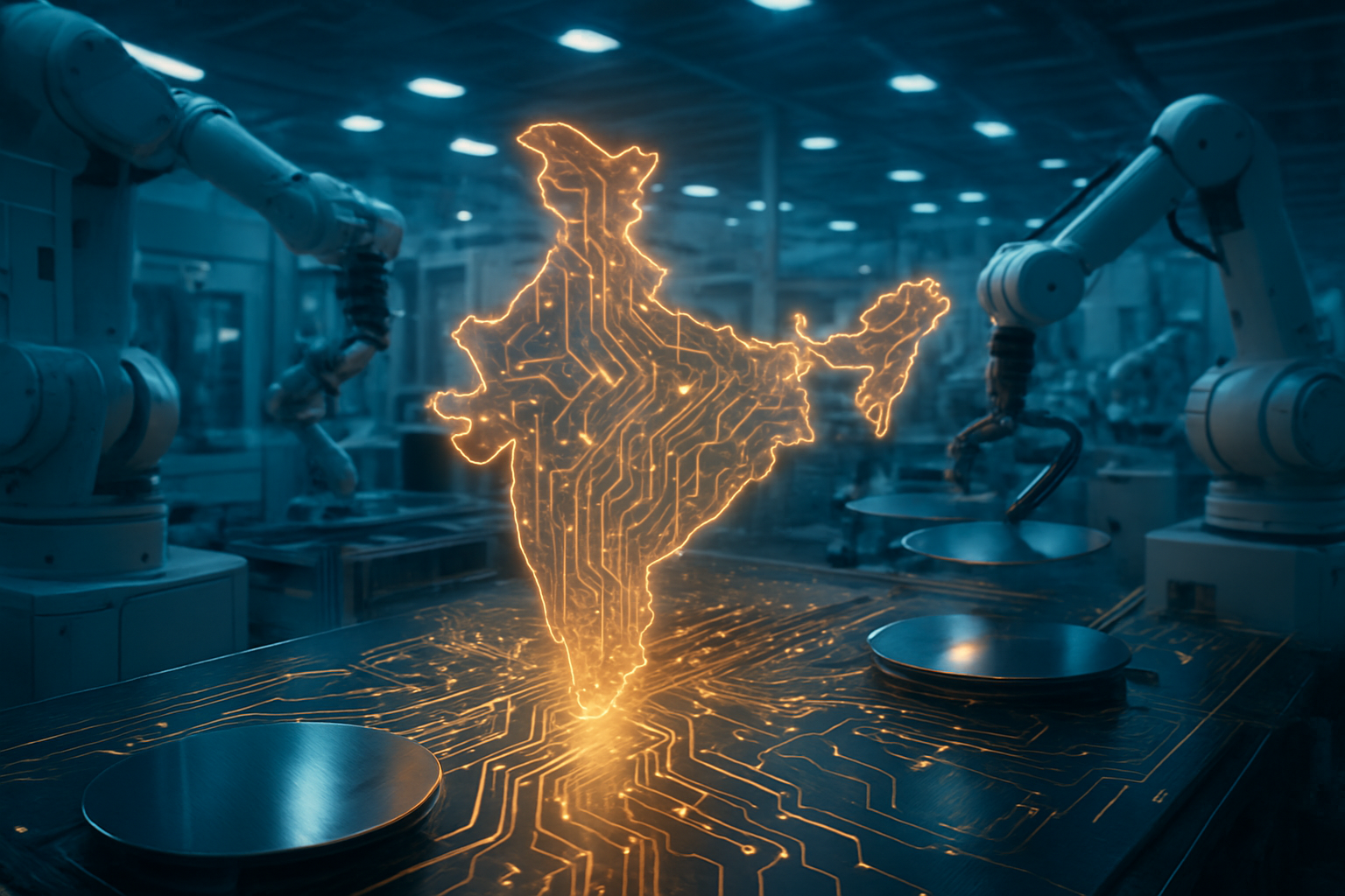
    New Delhi, India – December 8, 2025 – In a landmark strategic alliance poised to redefine the global semiconductor supply chain and catapult India onto the world stage of advanced manufacturing, Intel Corporation (NASDAQ: INTC) and the Tata Group announced a monumental collaboration today. This partnership centers around Tata Electronics' ambitious $14 billion (approximately ₹1.18 lakh crore) investment to establish India's first semiconductor fabrication (fab) facility in Dholera, Gujarat, and an Outsourced Semiconductor Assembly and Test (OSAT) plant in Assam. Intel is slated to be a pivotal initial customer for these facilities, exploring local manufacturing and packaging of its products, with a significant focus on rapidly scaling tailored AI PC solutions for the burgeoning Indian market.

    The agreement, formalized through a Memorandum of Understanding (MoU) on this date, marks a critical juncture for both entities. For Intel, it represents a strategic expansion of its global foundry services (IFS) and a diversification of its manufacturing footprint, particularly in a market projected to be a top-five global compute hub by 2030. For India, it’s a giant leap towards technological self-reliance and the realization of its "India Semiconductor Mission," aiming to create a robust, geo-resilient electronics and semiconductor ecosystem within the country.

    Technical Deep Dive: India's New Silicon Frontier and Intel's Foundry Ambitions

    The technical underpinnings of this deal are substantial, laying the groundwork for a new era of chip manufacturing in India. Tata Electronics, in collaboration with Taiwan's Powerchip Semiconductor Manufacturing Corporation (PSMC), is spearheading the Dholera fab, which is designed to produce chips using 28nm to 110nm technologies. These mature process nodes are crucial for a vast array of essential components, including power management ICs, display drivers, and microcontrollers, serving critical sectors such as automotive, IoT, consumer electronics, and industrial applications. The Dholera facility is projected to achieve a significant monthly production capacity of up to 50,000 wafers (300mm or 12-inch wafers).

    Beyond wafer fabrication, Tata is also establishing an advanced Outsourced Semiconductor Assembly and Test (OSAT) facility in Assam. This facility will be a key area of collaboration with Intel, exploring advanced packaging solutions in India. The total investment by Tata Electronics for these integrated facilities stands at approximately $14 billion. While the Dholera fab is slated for operations by mid-2027, the Assam OSAT facility could go live as early as April 2026, accelerating India's entry into the crucial backend of chip manufacturing.

    This alliance is a cornerstone of Intel's broader IDM 2.0 strategy, positioning Intel Foundry Services (IFS) as a "systems foundry for the AI era." Intel aims to offer full-stack optimization, from factory networks to software, leveraging its extensive engineering expertise to provide comprehensive manufacturing, advanced packaging, and integration services. By securing Tata as a key initial customer, Intel demonstrates its commitment to diversifying its global manufacturing capabilities and tapping into the rapidly growing Indian market, particularly for AI PC solutions. While the initial focus on 28nm-110nm nodes may not be Intel's cutting-edge (like its 18A or 14A processes), it strategically allows Intel to leverage these facilities for specific regional needs, packaging innovations, and to secure a foothold in a critical emerging market.

    Initial reactions from industry experts are largely positive, recognizing the strategic importance of the deal for both Intel and India. Experts laud the Indian government's strong support through initiatives like the India Semiconductor Mission, which makes such investments attractive. The appointment of former Intel Foundry Services President, Randhir Thakur, as CEO and Managing Director of Tata Electronics, underscores the seriousness of Tata's commitment and brings invaluable global expertise to India's burgeoning semiconductor ecosystem. While the focus on mature nodes is a practical starting point, it's seen as foundational for India to build robust manufacturing capabilities, which will be vital for a wide range of applications, including those at the edge of AI.

    Corporate Chessboard: Shifting Dynamics for Tech Giants and Startups

    The Intel-Tata alliance sends ripples across the corporate chessboard, promising to redefine competitive landscapes and open new avenues for growth, particularly in India.

    Tata Group (NSE: TATA) stands as a primary beneficiary. This deal is a monumental step in its ambition to become a global force in electronics and semiconductors. It secures a foundational customer in Intel and provides critical technology transfer for manufacturing and advanced packaging, positioning Tata Electronics across Electronics Manufacturing Services (EMS), OSAT, and semiconductor foundry services. For Intel (NASDAQ: INTC), this partnership significantly strengthens its Intel Foundry business by diversifying its supply chain and providing direct access to the rapidly expanding Indian market, especially for AI PCs. It's a strategic move to re-establish Intel as a major global foundry player.

    The implications for Indian AI companies and startups are profound. Local fab and OSAT facilities could dramatically reduce reliance on imports, potentially lowering costs and improving turnaround times for specialized AI chips and components. This fosters an innovation hub for indigenous AI hardware, leading to custom AI chips tailored for India's unique market needs, including multilingual processing. The anticipated creation of thousands of direct and indirect jobs will also boost the skilled workforce in semiconductor manufacturing and design, a critical asset for AI development. Even global tech giants with significant operations in India stand to benefit from a more localized and resilient supply chain for components.

    For major global AI labs like Google DeepMind, OpenAI, Meta AI (NASDAQ: META), and Microsoft AI (NASDAQ: MSFT), the direct impact on sourcing cutting-edge AI accelerators (e.g., advanced GPUs) from this specific fab might be limited initially, given its focus on mature nodes. However, the deal contributes to the overall decentralization of chip manufacturing, enhancing global supply chain resilience and potentially freeing up capacity at advanced fabs for leading-edge AI chips. The emergence of a robust Indian AI hardware ecosystem could also lead to Indian startups developing specialized AI chips for edge AI, IoT, or specific Indian language processing, which major AI labs might integrate into their products for the Indian market. The growth of India's sophisticated semiconductor industry will also intensify global competition for top engineering and research talent.

    Potential disruptions include a gradual shift in the geopolitical landscape of chip manufacturing, reducing over-reliance on concentrated hubs. The new capacity for mature node chips could introduce new competition for existing manufacturers, potentially leading to price adjustments. For Intel Foundry, securing Tata as a customer strengthens its position against pure-play foundries like TSMC (NYSE: TSM) and Samsung (KRX: 005930), albeit in different technology segments initially. This deal also provides massive impetus to India's "Make in India" initiatives, potentially encouraging more global companies to establish manufacturing footprints across various tech sectors in the country.

    A New Era: Broader Implications for Global Tech and Geopolitics

    The Intel-Tata semiconductor fab deal transcends mere corporate collaboration; it is a profound development with far-reaching implications for the broader AI landscape, global semiconductor supply chains, and international geopolitics.

    This collaboration is deeply integrated into the burgeoning AI landscape. The explicit goal to rapidly scale tailored AI PC solutions for the Indian market underscores the foundational role of semiconductors in driving AI adoption. India is projected to be among the top five global markets for AI PCs by 2030, and the chips produced at Tata's new facilities will cater to this escalating demand, alongside applications in automotive, wireless communication, and general computing. Furthermore, the manufacturing facilities themselves are envisioned to incorporate advanced automation powered by AI, machine learning, and data analytics to optimize efficiency, showcasing AI's pervasive influence even in its own production. Intel's CEO has highlighted that AI is profoundly transforming the world, creating an unprecedented opportunity for its foundry business, making this deal a critical component of Intel's long-term AI strategy.

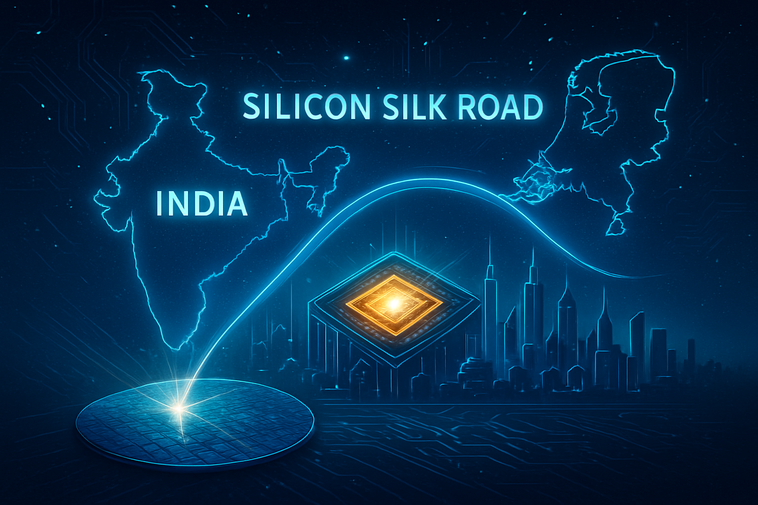
    The most immediate and significant impact will be on global semiconductor supply chains. This deal is a strategic move towards creating a more resilient and diversified global supply chain, a critical objective for many nations following recent disruptions. By establishing a significant manufacturing base in India, the initiative aims to rebalance the heavy concentration of chip production in regions like China and Taiwan, positioning India as a "second base" for manufacturing. This diversification mitigates vulnerabilities to geopolitical tensions, natural disasters, or unforeseen bottlenecks, contributing to a broader "tech decoupling" effort by Western nations to reduce reliance on specific regions. India's focus on manufacturing, including legacy chips, aims to establish it as a reliable and stable supplier in the global chip value chain.

    Geopolitically, the deal carries immense weight. India's Prime Minister Narendra Modi's "India Semiconductor Mission," backed by $10 billion in incentives, aims to transform India into a global chipmaker, rivaling established powerhouses. This collaboration is seen by some analysts as part of a "geopolitical game" where countries seek to diversify semiconductor sources and reduce Chinese dominance by supporting manufacturing in "like-minded countries" such as India. Domestic chip manufacturing enhances a nation's "digital sovereignty" and provides "digital leverage" on the global stage, bolstering India's self-reliance and influence. The historical concentration of advanced semiconductor production in Taiwan has been a source of significant geopolitical risk, making the diversification of manufacturing capabilities an imperative.

    However, potential concerns temper the optimism. Semiconductor manufacturing is notoriously capital-intensive, with long lead times to profitability. Intel itself has faced significant challenges and delays in its manufacturing transitions, impacting its market dominance. The specific logistical challenges in India, such as the need for "elephant-proof" walls in Assam to prevent vibrations from affecting nanometer-level precision, highlight the unique hurdles. Comparing this to previous milestones, Intel's past struggles in AI and manufacturing contrast sharply with Nvidia's rise and TSMC's dominance. This current global push for diversified manufacturing, exemplified by the Intel-Tata deal, marks a significant departure from earlier periods of increased reliance on globalized supply chains. Unlike past stalled attempts by India to establish chip fabrication, the current government incentives and the substantial commitment from Tata, coupled with international partnerships, represent a more robust and potentially successful approach.

    The Road Ahead: Challenges and Opportunities for India's Silicon Dream

    The Intel-Tata semiconductor fab deal, while groundbreaking, sets the stage for a future fraught with both immense opportunities and significant challenges for India's burgeoning silicon dream.

    In the near-term, the focus will be on the successful establishment and operationalization of Tata Electronics' facilities. The Assam OSAT plant is expected to be operational by mid-2025, followed by the Dholera fab commencing operations by 2027. Intel's role as the first major customer will be crucial, with initial efforts centered on manufacturing and packaging Intel products specifically for the Indian market and developing advanced packaging capabilities. This period will be critical for demonstrating India's capability in high-volume, high-precision manufacturing.

    Long-term developments envision a comprehensive silicon and compute ecosystem in India. Beyond merely manufacturing, the partnership aims to foster innovation, attract further investment, and position India as a key player in a geo-resilient global supply chain. This will necessitate significant skill development, with projections of tens of thousands of direct and indirect jobs, addressing the current gap in specialized semiconductor fabrication and testing expertise within India's workforce. The success of this venture could catalyze further foreign investment and collaborations, solidifying India's position in the global electronics supply chain.

    The potential applications for the chips produced are vast, with a strong emphasis on the future of AI. The rapid scaling of tailored AI PC solutions for India's consumer and enterprise markets is a primary objective, leveraging Intel's AI compute designs and Tata's manufacturing prowess. These chips will also fuel growth in industrial applications, general consumer electronics, and the automotive sector. India's broader "India Semiconductor Mission" targets the production of its first indigenous semiconductor chip by 2025, a significant milestone for domestic capability.

    However, several challenges need to be addressed. India's semiconductor industry currently grapples with an underdeveloped supply chain, lacking critical raw materials like silicon wafers, high-purity gases, and ultrapure water. A significant shortage of specialized talent for fabrication and testing, despite a strong design workforce, remains a hurdle. As a relatively late entrant, India faces stiff competition from established global hubs with decades of experience and mature ecosystems. Keeping pace with rapidly evolving technology and continuous miniaturization in chip design will demand continuous, substantial capital investments. Past attempts by India to establish chip manufacturing have also faced setbacks, underscoring the complexities involved.

    Expert predictions generally paint an optimistic picture, with India's semiconductor market projected to reach $64 billion by 2026 and approximately $103.4 billion by 2030, driven by rising PC demand and rapid AI adoption. Tata Sons Chairman N Chandrasekaran emphasizes the group's deep commitment to developing a robust semiconductor industry in India, seeing the alliance with Intel as an accelerator to capture the "large and growing AI opportunity." The strong government backing through the India Semiconductor Mission is seen as a key enabler for this transformation. The success of the Intel-Tata partnership could serve as a powerful blueprint, attracting further foreign investment and collaborations, thereby solidifying India's position in the global electronics supply chain.

    Conclusion: India's Semiconductor Dawn and Intel's Strategic Rebirth

    The strategic alliance between Intel Corporation (NASDAQ: INTC) and the Tata Group (NSE: TATA), centered around a $14 billion investment in India's semiconductor manufacturing capabilities, marks an inflection point for both entities and the global technology landscape. This monumental deal, announced on December 8, 2025, is a testament to India's burgeoning ambition to become a self-reliant hub for advanced technology and Intel's strategic re-commitment to its foundry business.

    The key takeaways from this development are multifaceted. For India, it’s a critical step towards establishing an indigenous, geo-resilient semiconductor ecosystem, significantly reducing its reliance on global supply chains. For Intel, it represents a crucial expansion of its Intel Foundry Services, diversifying its manufacturing footprint and securing a foothold in one of the world's fastest-growing compute markets, particularly for AI PC solutions. The collaboration on mature node manufacturing (28nm-110nm) and advanced packaging will foster a comprehensive ecosystem, from design to assembly and test, creating thousands of skilled jobs and attracting further investment.

    Assessing this development's significance in AI history, it underscores the fundamental importance of hardware in the age of artificial intelligence. While not directly producing cutting-edge AI accelerators, the establishment of robust, diversified manufacturing capabilities is essential for the underlying components that power AI-driven devices and infrastructure globally. This move aligns with a broader trend of "tech decoupling" and the decentralization of critical manufacturing, enhancing global supply chain resilience and mitigating geopolitical risks associated with concentrated production. It signals a new chapter for Intel's strategic rebirth and India's emergence as a formidable player in the global technology arena.

    Looking ahead, the long-term impact promises to be transformative for India's economy and technological sovereignty. The successful operationalization of these fabs and OSAT facilities will not only create direct economic value but also foster an innovation ecosystem that could spur indigenous AI hardware development. However, challenges related to supply chain maturity, talent development, and intense global competition will require sustained effort and investment. What to watch for in the coming weeks and months includes further details on technology transfer, the progress of facility construction, and the initial engagement of Intel as a customer. The success of this venture will be a powerful indicator of India's capacity to deliver on its high-tech ambitions and Intel's ability to execute its revitalized foundry strategy.


    This content is intended for informational purposes only and represents analysis of current AI developments.

    TokenRing AI delivers enterprise-grade solutions for multi-agent AI workflow orchestration, AI-powered development tools, and seamless remote collaboration platforms.
    For more information, visit https://www.tokenring.ai/.

  • TSMC’s Unstoppable Momentum: Billions Poured into Global Expansion as AI Fuels Investor Frenzy

    TSMC’s Unstoppable Momentum: Billions Poured into Global Expansion as AI Fuels Investor Frenzy

    Taiwan Semiconductor Manufacturing Company (NYSE: TSM), the undisputed titan of the global semiconductor foundry industry, is experiencing an unprecedented surge in investment and investor confidence as of November 2025. Driven by an insatiable demand for cutting-edge chips powering the artificial intelligence revolution, TSMC is aggressively expanding its manufacturing footprint and technological capabilities worldwide, solidifying its indispensable role in the digital economy. This wave of capital expenditure and robust financial performance underscores the company's critical importance in shaping the future of technology.

    The immediate significance of TSMC's current trajectory cannot be overstated. With projected capital expenditures for 2025 ranging between $38 billion and $42 billion, the company is making a clear statement of intent: to maintain its technological leadership and meet the escalating global demand for advanced semiconductors. This substantial investment is primarily directed towards advanced process development, ensuring TSMC remains at the forefront of chip manufacturing, a position that is increasingly vital for tech giants and innovative startups alike.

    Engineering the Future: TSMC's Technological Edge and Strategic Investments

    TSMC's strategic investment initiatives are meticulously designed to reinforce its technological dominance and cater to the evolving needs of the high-performance computing (HPC) and AI sectors. Approximately 70% of its massive capital expenditure is funneled into advanced process development, with a significant portion dedicated to bringing 2-nanometer (nm) technology to mass production. The company anticipates commencing mass production of 2nm chips in the second half of 2025, with an ambitious target of reaching a monthly production capacity of up to 90,000 wafers by late 2026. This technological leap promises a 25-30% improvement in energy efficiency, a critical factor for power-hungry AI applications, and is expected to further boost TSMC's margins and secure long-term contracts.

    Beyond process node advancements, TSMC is also aggressively scaling its advanced packaging capabilities, recognizing their crucial role in integrating complex AI and HPC chips. Its Chip-on-Wafer-on-Substrate (CoWoS) capacity is projected to expand by over 80% from 2022 to 2026, while its System-on-Integrated-Chip (SoIC) capacity is expected to grow at a compound annual growth rate (CAGR) exceeding 100% during the same period. These packaging innovations are vital for overcoming the physical limitations of traditional chip design, allowing for denser, more powerful, and more efficient integration of components—a key differentiator from previous approaches and a necessity for the next generation of AI hardware.

    The company's global footprint expansion is equally ambitious. In Taiwan, seven new facilities are slated for 2025, including 2nm production bases in Hsinchu and Kaohsiung, and advanced packaging facilities across Tainan, Taichung, and Chiayi. Internationally, TSMC is dramatically increasing its investment in the United States to a staggering total of US$165 billion, establishing three new fabrication plants, two advanced packaging facilities, and a major R&D center in Phoenix, Arizona. Construction of its second Kumamoto fab in Japan is set to begin in Q1 2025, with mass production targeted for 2027, and progress continues on a new fab in Dresden, Germany. These expansions demonstrate a commitment to diversify its manufacturing base while maintaining its technological lead, a strategy that sets it apart from competitors who often struggle to match the scale and complexity of TSMC's advanced manufacturing.

    The AI Engine: How TSMC's Dominance Shapes the Tech Landscape

    TSMC's unparalleled manufacturing capabilities are not just a technical marvel; they are the bedrock upon which the entire AI industry is built, profoundly impacting tech giants, AI companies, and startups alike. Companies like Apple (NASDAQ: AAPL), NVIDIA (NASDAQ: NVDA), Advanced Micro Devices (NASDAQ: AMD), Broadcom (NASDAQ: AVGO), and Qualcomm (NASDAQ: QCOM) are heavily reliant on TSMC for the production of their most advanced semiconductors. This dependence means that TSMC's technological advancements and production capacity directly dictate the pace of innovation and product launches for these industry leaders.

    For major AI labs and tech companies, TSMC's leading-edge process technologies are critical enablers. The company's 3nm chips currently power Apple's latest devices, and its upcoming 2nm technology is expected to be crucial for the next generation of AI accelerators and high-performance processors. This ensures that companies at the forefront of AI development have access to the most power-efficient and high-performing chips, giving them a competitive edge. Without TSMC's capabilities, the rapid advancements seen in areas like large language models, autonomous systems, and advanced graphics processing would be significantly hampered.

    The competitive implications are clear: companies with strong partnerships and allocation at TSMC stand to benefit immensely. This creates a strategic advantage for those who can secure manufacturing slots for their innovative chip designs. Conversely, any disruption or bottleneck at TSMC could have cascading effects across the entire tech ecosystem, impacting product availability, development timelines, and market positioning. TSMC's consistent delivery and technological leadership minimize such risks, providing a stable and advanced manufacturing partner that is essential for the sustained growth of the AI and tech sectors.

    Global Geopolitics and the Silicon Backbone: Wider Significance of TSMC

    TSMC's role extends far beyond merely manufacturing chips; it is a linchpin of global technology, intertwining with geopolitical stability, economic prosperity, and the broader trajectory of technological advancement. The company's unchallenged market leadership, commanding an estimated 70% of the global chip manufacturing market and over 55% of the foundry sector in 2024, makes it a critical component of international supply chains. This technological indispensability means that major world economies and their leading tech firms are deeply invested in TSMC's success and stability.

    The company's extensive investments and global expansion efforts, particularly in the United States, Japan, and Europe, are not just about increasing capacity; they are strategic moves to de-risk supply chains and foster localized semiconductor ecosystems. The expanded investment in the U.S. alone is projected to create 40,000 construction jobs and tens of thousands of high-paying, high-tech manufacturing and R&D positions, driving over $200 billion of indirect economic output. This demonstrates the profound economic ripple effect of TSMC's operations and its significant contribution to global employment and innovation.

    Concerns about geopolitical tensions, particularly in the Taiwan Strait, inevitably cast a shadow over TSMC's valuation. However, the global reliance on its manufacturing capabilities acts as a mitigating factor, making its stability a shared international interest. The company's consistent innovation, as recognized by the Robert N. Noyce Award presented to its Chairman C.C. Wei and former Chairman Mark Liu in November 2025, underscores its profound contributions to the semiconductor industry, comparable to previous milestones that defined eras of computing. TSMC's advancements are not just incremental; they are foundational, enabling the current AI boom and setting the stage for future technological breakthroughs.

    The Road Ahead: Future Developments and Enduring Challenges

    Looking ahead, TSMC's trajectory is marked by continued aggressive expansion and relentless pursuit of next-generation technologies. The company's commitment to mass production of 2nm chips by the second half of 2025 and its ongoing research into even more advanced nodes signal a clear path towards sustained technological leadership. The planned construction of additional 2nm factories in Taiwan and the significant investments in advanced packaging facilities like CoWoS and SoIC are expected to further solidify its position as the go-to foundry for the most demanding AI and HPC applications.

    Potential applications and use cases on the horizon are vast, ranging from more powerful and efficient AI accelerators for data centers to advanced chips for autonomous vehicles, augmented reality devices, and ubiquitous IoT. Experts predict that TSMC's innovations will continue to push the boundaries of what's possible in computing, enabling new forms of intelligence and connectivity. The company's focus on energy efficiency in its next-generation processes is particularly crucial as AI workloads become increasingly resource-intensive, addressing a key challenge for sustainable technological growth.

    However, challenges remain. The immense capital expenditure required to stay ahead in the semiconductor race necessitates sustained profitability and access to talent. Geopolitical risks, while mitigated by global reliance, will continue to be a factor. Competition, though currently lagging in advanced nodes, could intensify in the long term. What experts predict will happen next is a continued arms race in semiconductor technology, with TSMC leading the charge, but also a growing emphasis on resilient supply chains and diversified manufacturing locations to mitigate global risks. The company's strategic global expansion is a direct response to these challenges, aiming to build a more robust and distributed manufacturing network.

    A Cornerstone of the AI Era: Wrapping Up TSMC's Impact

    In summary, TSMC's current investment trends and investor interest reflect its pivotal and increasingly indispensable role in the global technology landscape. Key takeaways include its massive capital expenditures directed towards advanced process nodes like 2nm and sophisticated packaging technologies, overwhelmingly positive investor sentiment fueled by robust financial performance and its critical role in the AI boom, and its strategic global expansion to meet demand and mitigate risks. The company's recent 17% increase in its quarterly dividend further signals confidence in its sustained growth and profitability.

    This development's significance in AI history is profound. TSMC is not just a manufacturer; it is the silent enabler of the AI revolution, providing the foundational hardware that powers everything from sophisticated algorithms to complex neural networks. Without its continuous innovation and manufacturing prowess, the rapid advancements in AI that we witness today would be severely constrained. Its technological leadership and market dominance make it a cornerstone of the modern digital age.

    Final thoughts on the long-term impact point to TSMC remaining a critical barometer for the health and direction of the tech industry. Its ability to navigate geopolitical complexities, maintain its technological edge, and continue its aggressive expansion will largely determine the pace of innovation for decades to come. What to watch for in the coming weeks and months includes further updates on its 2nm production ramp-up, progress on its global fab constructions, and any shifts in its capital expenditure guidance, all of which will provide further insights into the future of advanced semiconductor manufacturing and, by extension, the future of AI.


    This content is intended for informational purposes only and represents analysis of current AI developments.

    TokenRing AI delivers enterprise-grade solutions for multi-agent AI workflow orchestration, AI-powered development tools, and seamless remote collaboration platforms.
    For more information, visit https://www.tokenring.ai/.

  • The Global Chip Renaissance: Billions Poured into New Fabs as Manufacturing Shifts Reshape Tech Landscape

    The Global Chip Renaissance: Billions Poured into New Fabs as Manufacturing Shifts Reshape Tech Landscape

    The global semiconductor industry is in the midst of an unprecedented building boom, with chipmakers and governments worldwide committing trillions of dollars to construct new fabrication plants (fabs) and expand existing facilities. This massive wave of investment, projected to exceed $1.5 trillion between 2024 and 2030, is not merely about increasing capacity; it represents a fundamental restructuring of the global supply chain, driven by escalating demand for advanced chips in artificial intelligence (AI), 5G, high-performance computing (HPC), and the burgeoning automotive sector. The immediate significance lies in a concerted effort to enhance supply chain resilience, accelerate technological advancement, and secure national economic and technological leadership.

    This transformative period, heavily influenced by geopolitical considerations and robust government incentives like the U.S. CHIPS and Science Act, is seeing a strategic rebalancing of manufacturing hubs. While Asia remains dominant, North America and Europe are experiencing a significant resurgence, with major players like Taiwan Semiconductor Manufacturing Company (TSMC) (NYSE: TSM), Intel (NASDAQ: INTC), and Samsung (KRX: 005930) leading the charge in establishing state-of-the-art facilities across multiple continents. The scale and speed of these investments underscore a global recognition of semiconductors as the bedrock of modern economies and future innovation.

    The Technical Crucible: Forging the Next Generation of Silicon

    The heart of this global expansion lies in the relentless pursuit of advanced process technologies and specialized manufacturing capabilities. Companies are not just building more fabs; they are building highly sophisticated facilities designed to produce the most cutting-edge chips, often pushing the boundaries of physics and engineering. This includes the development of 2nm, 1.8nm, and even future 1.6nm nodes, alongside significant advancements in High-Bandwidth Memory (HBM) and advanced packaging solutions like CoWoS and SoIC, which are crucial for AI accelerators and other high-performance applications.

    TSMC, the undisputed leader in contract chip manufacturing, is at the forefront, with plans for 10 new and ongoing fab projects globally by 2025. This includes four 2nm production sites in Taiwan and significant expansion of advanced packaging capacity, expected to double in 2024 and increase by another 30% in 2025. Their $165 billion commitment in the U.S. for three new fabs, two advanced packaging facilities, and an R&D center, and new fabs in Japan and Germany, highlight a multi-pronged approach to global leadership. Intel, aiming to reclaim its process technology crown, is investing over $100 billion over five years in the U.S., with new fabs in Arizona and Ohio targeting 2nm and 1.8nm technologies by 2025-2026. Samsung, not to be outdone, is pouring approximately $309-$310 billion into South Korea over the next five years for advanced R&D and manufacturing, including its fifth plant at Pyeongtaek Campus and a new R&D complex, alongside a $40 billion investment in Central Texas for a new fab.

    These new facilities often incorporate extreme ultraviolet (EUV) lithography, a technology critical for manufacturing advanced nodes, representing a significant technical leap from previous approaches. The investment in EUV machines alone runs into hundreds of millions of dollars per unit, showcasing the immense capital intensity of modern chipmaking. The industry is also seeing a surge in specialized technologies, such as silicon-carbide (SiC) and gallium-nitride (GaN) semiconductors for electric vehicles and power electronics, reflecting a diversification beyond general-purpose logic and memory. Initial reactions from the AI research community and industry experts emphasize that these investments are vital for sustaining the exponential growth of AI and other data-intensive applications, providing the foundational hardware necessary for future breakthroughs. The scale and complexity of these projects are unprecedented, requiring massive collaboration between governments, chipmakers, and equipment suppliers.

    Shifting Sands: Corporate Strategies and Competitive Implications

    The global semiconductor manufacturing expansion is profoundly reshaping the competitive landscape, creating both immense opportunities and significant challenges for AI companies, tech giants, and startups alike. Companies with strong balance sheets and strategic government partnerships are best positioned to capitalize on this boom. TSMC, Intel, and Samsung are clearly the primary beneficiaries, as their aggressive expansion plans are cementing their roles as foundational suppliers of advanced chips.

    For AI companies and tech giants like Nvidia (NASDAQ: NVDA), Google (NASDAQ: GOOGL), Microsoft (NASDAQ: MSFT), and Amazon (NASDAQ: AMZN), these investments translate into a more robust and geographically diversified supply of the high-performance chips essential for their AI models and data centers. A more resilient supply chain reduces the risk of future shortages and allows for greater innovation in AI hardware. However, it also means potentially higher costs for advanced nodes as manufacturing shifts to higher-cost regions like the U.S. and Europe. Startups in AI and specialized hardware may face increased competition for fab access, but could also benefit from new foundry services and specialized process technologies becoming available closer to home.

    The competitive implications are stark. Intel's ambitious "IDM 2.0" strategy, focusing on both internal product manufacturing and external foundry services, directly challenges TSMC and Samsung's dominance in contract manufacturing. If successful, Intel Foundry Services could disrupt the existing foundry market, offering an alternative for companies seeking to diversify their chip production. Similarly, Samsung's aggressive push into advanced packaging and memory, alongside its foundry business, intensifies the rivalry across multiple segments. The focus on regional self-sufficiency could also lead to fragmentation, with different fabs specializing in certain types of chips or serving specific regional markets, potentially impacting global standardization and economies of scale.

    A New Era of Geopolitical Chipmaking

    The current wave of semiconductor manufacturing expansion is more than just an industrial phenomenon; it's a geopolitical imperative. This massive investment cycle fits squarely into the broader AI landscape and global trends of technological nationalism and supply chain de-risking. Nations worldwide recognize that control over advanced semiconductor manufacturing is tantamount to national security and economic sovereignty in the 21st century. The U.S. CHIPS Act, along with similar initiatives in Europe and Japan, explicitly aims to reduce reliance on concentrated manufacturing in Asia, particularly Taiwan, which produces the vast majority of advanced logic chips.

    The impacts are wide-ranging. Economically, these investments are creating tens of thousands of high-paying jobs in construction, manufacturing, and R&D across various regions, fostering local semiconductor ecosystems. Strategically, they aim to enhance supply chain resilience against disruptions, whether from natural disasters, pandemics, or geopolitical tensions. However, potential concerns include the immense cost of these endeavors, the risk of overcapacity in the long term, and the challenge of securing enough skilled labor to staff these advanced fabs. The environmental impact of building and operating such energy-intensive facilities also remains a significant consideration.

    Comparisons to previous AI milestones highlight the foundational nature of this development. While breakthroughs in AI algorithms and software often capture headlines, the ability to physically produce the hardware capable of running these advanced algorithms is equally, if not more, critical. This manufacturing expansion is akin to building the superhighways and power grids necessary for the digital economy, enabling the next generation of AI to scale beyond current limitations. It represents a global race not just for technological leadership, but for industrial capacity itself, reminiscent of historical industrial revolutions.

    The Road Ahead: Challenges and Opportunities

    Looking ahead, the semiconductor industry is poised for continued rapid evolution, with several key developments on the horizon. Near-term, the focus will remain on bringing the multitude of new fabs online and ramping up production of 2nm and 1.8nm chips. We can expect further advancements in advanced packaging technologies, which are becoming increasingly critical for extracting maximum performance from individual chiplets. The integration of AI directly into the chip design and manufacturing process itself will also accelerate, leading to more efficient and powerful chip architectures.

    Potential applications and use cases on the horizon are vast. Beyond current AI accelerators, these advanced chips will power truly ubiquitous AI, enabling more sophisticated autonomous systems, hyper-realistic metaverse experiences, advanced medical diagnostics, and breakthroughs in scientific computing. The automotive sector, in particular, will see a dramatic increase in chip content as vehicles become software-defined and increasingly autonomous. Challenges that need to be addressed include the persistent talent gap in semiconductor engineering and manufacturing, the escalating costs of R&D and equipment, and the complexities of managing a geographically diversified but interconnected supply chain. Geopolitical tensions, particularly concerning access to advanced lithography tools and intellectual property, will also continue to shape investment decisions.

    Experts predict that the drive for specialization will intensify, with different regions potentially focusing on specific types of chips – for instance, the U.S. on leading-edge logic, Europe on power semiconductors, and Asia maintaining its dominance in memory and certain logic segments. The "fabless" model, where companies design chips but outsource manufacturing, will continue, but with more options for where to fabricate, potentially leading to more customized supply chain strategies. The coming years will be defined by the industry's ability to balance rapid innovation with sustainable, resilient manufacturing.

    Concluding Thoughts: A Foundation for the Future

    The global semiconductor manufacturing expansion is arguably one of the most significant industrial undertakings of the 21st century. The sheer scale of investment, the ambitious technological goals, and the profound geopolitical implications underscore its importance. This isn't merely a cyclical upturn; it's a fundamental re-architecture of a critical global industry, driven by the insatiable demand for processing power, especially from the burgeoning field of artificial intelligence.

    The key takeaways are clear: a massive global capital expenditure spree is underway, leading to significant regional shifts in manufacturing capacity. This aims to enhance supply chain resilience, fuel technological advancement, and secure national economic leadership. While Asia retains its dominance, North America and Europe are making substantial inroads, creating a more distributed, albeit potentially more complex, global chip ecosystem. The significance of this development in AI history cannot be overstated; it is the physical manifestation of the infrastructure required for the next generation of intelligent machines.

    In the coming weeks and months, watch for announcements regarding the operational status of new fabs, further government incentives, and how companies navigate the intricate balance between global collaboration and national self-sufficiency. The long-term impact will be a more robust and diversified semiconductor supply chain, but one that will also be characterized by intense competition and ongoing geopolitical maneuvering. The future of AI, and indeed the entire digital economy, is being forged in these new, advanced fabrication plants around the world.


    This content is intended for informational purposes only and represents analysis of current AI developments.

    TokenRing AI delivers enterprise-grade solutions for multi-agent AI workflow orchestration, AI-powered development tools, and seamless remote collaboration platforms.
    For more information, visit https://www.tokenring.ai/.

  • Malaysia’s Ambitious Leap: Forging a New Era in Global Semiconductor Design and Advanced Manufacturing

    Malaysia’s Ambitious Leap: Forging a New Era in Global Semiconductor Design and Advanced Manufacturing

    Malaysia is rapidly recalibrating its position in the global semiconductor landscape, embarking on an audacious strategic push to ascend the value chain beyond its traditional stronghold in assembly, testing, and packaging (ATP). This concerted national effort, backed by substantial investments and a visionary National Semiconductor Strategy (NSS), signifies a pivotal shift towards becoming a comprehensive semiconductor hub encompassing integrated circuit (IC) design, advanced manufacturing, and high-end wafer fabrication. The immediate significance of this pivot is profound, positioning Malaysia as a critical player in fostering a more resilient and diversified global chip supply chain amidst escalating geopolitical tensions and an insatiable demand for advanced silicon.

    The nation's ambition is not merely to be "Made in Malaysia" but to foster a "Designed by Malaysia" ethos, cultivating indigenous innovation and intellectual property. This strategic evolution is poised to attract a new wave of high-tech investments, create knowledge-based jobs, and solidify Malaysia's role as a trusted partner in the burgeoning era of artificial intelligence and advanced computing. With a clear roadmap and robust governmental support, Malaysia is proactively shaping its future as a high-value semiconductor ecosystem, ready to meet the complex demands of the 21st-century digital economy.

    The Technical Blueprint: From Backend to Brainpower

    Malaysia's strategic shift is underpinned by a series of concrete technical advancements and investment commitments designed to propel it into the forefront of advanced semiconductor capabilities. The National Semiconductor Strategy (NSS), launched in May 2024, acts as a dynamic three-phase roadmap, with Phase 1 focusing on modernizing existing outsourced semiconductor assembly and test (OSAT) capabilities and attracting high-end manufacturing equipment, while Phase 2 aims to attract foreign direct investment (FDI) in advanced chip manufacturing and develop local champions, ultimately leading to Phase 3's goal of establishing higher-end wafer fabrication facilities. This phased approach demonstrates a methodical progression towards full-spectrum semiconductor prowess.

    A cornerstone of this technical transformation is the aggressive development of Integrated Circuit (IC) design capabilities. The Malaysia Semiconductor IC Design Park in Puchong, launched in August 2024, stands as Southeast Asia's largest, currently housing over 200 engineers from 14 companies and providing state-of-the-art CAD tools, prototyping labs, and simulation environments. This initiative has already seen seven companies within the park actively involved in ARM CSS and AFA Design Token initiatives, with the ambitious target of developing Malaysia's first locally designed chip by 2027 or 2028. Further reinforcing this commitment, a second IC Design Park in Cyberjaya (IC Design Park 2) was launched in November 2025, featuring an Advanced Chip Testing Centre and training facilities under the Advanced Semiconductor Malaysia Academy (ASEM), backed by significant government funding and global partners like Arm, Synopsys, (NASDAQ: SNPS) Amazon Web Services (AWS), and Keysight (NYSE: KEYS).

    This differs significantly from Malaysia's historical role, which predominantly focused on the backend of the semiconductor process. By investing in IC design parks, securing advanced chip design blueprints from Arm Holdings (NASDAQ: ARM), and fostering local innovation, Malaysia is actively moving upstream, aiming to create intellectual property rather than merely assembling it. The RM3 billion facility expansion in Sarawak, launched in September 2025, boosting wafer production capacity from 30,000 to 40,000 units per month for automotive, medical, and industrial applications, further illustrates this move towards higher-value manufacturing. Initial reactions from the AI research community and industry experts have been largely positive, recognizing Malaysia's potential to become a crucial node in the global chip ecosystem, particularly given the increasing demand for specialized chips for AI, automotive, and IoT applications.

    Competitive Implications and Market Positioning

    Malaysia's strategic push carries significant competitive implications for major AI labs, tech giants, and startups alike. Companies like AMD (NASDAQ: AMD) are already planning advanced packaging and design operations in Penang, signaling a move beyond traditional backend work. Infineon Technologies AG (XTRA: IFX) is making a colossal €5 billion investment to build one of the world's largest silicon carbide power fabs in Kulim, a critical component for electric vehicles and industrial applications. Intel Corporation (NASDAQ: INTC) continues to expand its operations with a $7 billion advanced chip packaging plant in Malaysia. Other global players such as Micron Technology, Inc. (NASDAQ: MU), AT&S Austria Technologie & Systemtechnik AG (VIE: ATS), Texas Instruments Incorporated (NASDAQ: TXN), NXP Semiconductors N.V. (NASDAQ: NXPI), and Syntiant Corp. are also investing or expanding, particularly in advanced packaging and specialized chip production.

    These developments stand to benefit a wide array of companies. For established tech giants, Malaysia offers a stable and expanding ecosystem for diversifying their supply chains and accessing skilled talent for advanced manufacturing and design. For AI companies, the focus on developing local chip design capabilities, including the partnership with Arm to produce seven high-end chip blueprints for Malaysian companies, means a potential for more localized and specialized AI hardware development, potentially leading to cost efficiencies and faster innovation cycles. Startups in the IC design space are particularly poised to gain from the new design parks, incubators like the Penang Silicon Research and Incubation Space (PSD@5KM+), and funding initiatives such as the Selangor Semiconductor Fund, which aims to raise over RM100 million for high-potential local semiconductor design and technology startups.

    This strategic pivot could disrupt existing market dynamics by offering an alternative to traditional manufacturing hubs, fostering greater competition and potentially driving down costs for specialized components. Malaysia's market positioning is strengthened by its neutrality in geopolitical tensions, making it an attractive investment destination for companies seeking to de-risk their supply chains. The emphasis on advanced packaging and design also provides a strategic advantage, allowing Malaysia to capture a larger share of the value created in the semiconductor lifecycle, moving beyond its historical role as primarily an assembly point.

    Broader Significance and Global Trends

    Malaysia's aggressive foray into higher-value semiconductor activities fits seamlessly into the broader global AI landscape and prevailing technological trends. The insatiable demand for AI-specific hardware, from powerful GPUs to specialized AI accelerators, necessitates diversified and robust supply chains. As AI models grow in complexity and data processing requirements, the need for advanced packaging and efficient chip design becomes paramount. Malaysia's investments in these areas directly address these critical needs, positioning it as a key enabler for future AI innovation.

    The impacts of this strategy are far-reaching. It contributes to global supply chain resilience, reducing over-reliance on a few geographical regions for critical semiconductor components. This diversification is particularly crucial in an era marked by geopolitical uncertainties and the increasing weaponization of technology. Furthermore, by fostering local design capabilities and talent, Malaysia is contributing to a more distributed global knowledge base in semiconductor technology, potentially accelerating breakthroughs and fostering new collaborations.

    Potential concerns, however, include the intense global competition for skilled talent and the immense capital expenditure required for high-end wafer fabrication. While Malaysia is actively addressing talent development with ambitious training programs (e.g., 10,000 engineers in advanced chip design), sustaining this pipeline and attracting top-tier global talent will be an ongoing challenge. The comparison to previous AI milestones reveals a pattern: advancements in AI are often gated by the underlying hardware capabilities. By strengthening its semiconductor foundation, Malaysia is not just building chips; it's building the bedrock for the next generation of AI innovation, mirroring the foundational role played by countries like Taiwan and South Korea in previous computing eras.

    Future Developments and Expert Predictions

    In the near-term, Malaysia is expected to see continued rapid expansion in its IC design ecosystem, with the two major design parks in Puchong and Cyberjaya becoming vibrant hubs for innovation. The partnership with Arm is projected to yield its first locally designed high-end chips within the next two to three years (by 2027 or 2028), marking a significant milestone. We can also anticipate further foreign direct investment in advanced packaging and specialized manufacturing, as companies seek to leverage Malaysia's growing expertise and supportive ecosystem. The Advanced Semiconductor Malaysia Academy (ASEM) will likely ramp up its training programs, churning out a new generation of skilled engineers and technicians crucial for sustaining this growth.

    Longer-term developments, particularly towards Phase 3 of the NSS, will focus on attracting and establishing higher-end wafer fabrication facilities. While capital-intensive, the success in design and advanced packaging could create the necessary momentum and infrastructure for this ambitious goal. Potential applications and use cases on the horizon include specialized AI chips for edge computing, automotive AI, and industrial automation, where Malaysia's focus on power semiconductors and advanced packaging will be particularly relevant.

    Challenges that need to be addressed include maintaining a competitive edge in a rapidly evolving global market, ensuring a continuous supply of highly skilled talent, and navigating the complexities of international trade and technology policies. Experts predict that Malaysia's strategic push will solidify its position as a key player in the global semiconductor supply chain, particularly for niche and high-growth segments like silicon carbide and advanced packaging. The collaborative ecosystem, spearheaded by initiatives like the ASEAN Integrated Semiconductor Supply Chain Framework, suggests a future where regional cooperation further strengthens Malaysia's standing.

    A New Dawn for Malaysian Semiconductors

    Malaysia's strategic push in semiconductor manufacturing represents a pivotal moment in its economic history and a significant development for the global technology landscape. The key takeaways are clear: a determined shift from a backend-centric model to a comprehensive ecosystem encompassing IC design, advanced packaging, and a long-term vision for wafer fabrication. Massive investments, both domestic and foreign (exceeding RM63 billion or US$14.88 billion secured as of March 2025), coupled with a robust National Semiconductor Strategy and the establishment of state-of-the-art IC design parks, underscore the seriousness of this ambition.

    This development holds immense significance in AI history, as it directly addresses the foundational hardware requirements for the next wave of artificial intelligence innovation. By fostering a "Designed by Malaysia" ethos, the nation is not just participating but actively shaping the future of silicon, creating intellectual property and high-value jobs. The long-term impact is expected to transform Malaysia into a resilient and self-sufficient semiconductor hub, capable of supporting cutting-edge AI, automotive, and industrial applications.

    In the coming weeks and months, observers should watch for further announcements regarding new investments, the progress of companies within the IC design parks, and the tangible outcomes of the talent development programs. The successful execution of the NSS, particularly the development of locally designed chips and the expansion of advanced manufacturing capabilities, will be critical indicators of Malaysia's trajectory towards becoming a global leader in the advanced semiconductor sector. The world is witnessing a new dawn for Malaysian semiconductors, poised to power the innovations of tomorrow.


    This content is intended for informational purposes only and represents analysis of current AI developments.

    TokenRing AI delivers enterprise-grade solutions for multi-agent AI workflow orchestration, AI-powered development tools, and seamless remote collaboration platforms.
    For more information, visit https://www.tokenring.ai/.

  • TSMC’s Global Gambit: A Trillion-Dollar Bet on the Future of AI and Geopolitical Resilience

    TSMC’s Global Gambit: A Trillion-Dollar Bet on the Future of AI and Geopolitical Resilience

    Taiwan Semiconductor Manufacturing Company (NYSE: TSM), the undisputed titan of the semiconductor foundry industry, is embarking on an unprecedented global expansion and capital expenditure spree. With an eye towards securing its dominance in the burgeoning artificial intelligence (AI) and high-performance computing (HPC) sectors, and driven by profound geopolitical shifts, TSMC's investment strategy into 2025 and beyond signals a transformative era for the global technology supply chain. The company's audacious plans, involving tens of billions in annual capital expenditure and a record number of new facilities across three continents, underscore the critical importance of advanced chip manufacturing in the modern world.

    This monumental investment push is not merely about meeting demand; it is a strategic maneuver to navigate a complex geopolitical landscape, bolster supply chain resilience for nations, and solidify its technological lead. As the world races to build the infrastructure for the AI revolution, TSMC's decisions will reverberate through every corner of the tech industry, from the largest tech giants to agile startups.

    Unpacking TSMC's Unprecedented Investment Wave

    TSMC's capital expenditure (CapEx) projections for 2025 are nothing short of staggering, with forecasts ranging from US$34 billion to US$42 billion, potentially surpassing its previous peak of US$36.29 billion in 2022. This financial firepower is being directed towards an ambitious global construction program, comprising ten ongoing or newly launched projects by 2025 – a record for the company and the industry. Approximately 70% of this CapEx is earmarked for advanced technology production, while 10-20% will fuel specialty processes, and another 10-20% will enhance advanced packaging, testing, and mask manufacturing capabilities.

    Within Taiwan, the company is developing seven new facilities, including two 2nm production bases (with two fabs each in Hsinchu and Kaohsiung) and three advanced packaging facilities (AP8 in Tainan, CoWoS expansion in Taichung, and new CoWoS/SoIC investments in Chiayi). Mass production of 2nm chips is slated for the second half of 2025. Globally, TSMC is significantly expanding its footprint. In Arizona, USA, the total planned investment could reach an astounding US$165 billion, encompassing a first fab that began 4nm volume production in Q4 2024, a second 3nm fab with construction completed, and a third 2nm (or more advanced) fab that broke ground in April 2025. This U.S. expansion also includes plans for two advanced packaging facilities and a major R&D center. In Japan, the first fab in Kumamoto, a joint venture with Sony Semiconductor Solutions (TYO: 6758), DENSO (TYO: 6902), and Toyota (TYO: 7203), commenced mass production in late 2024. A second Kumamoto fab, focusing on 6nm, 7nm, and 40nm chips, is scheduled to begin construction in Q1 2025, targeting 2027 for mass production, with the total investment in JASM exceeding US$20 billion. Europe also enters the fray, with construction of TSMC's first European chip plant in Dresden, Germany, a joint venture with Infineon (ETR: IFX), NXP (NASDAQ: NXPI), and Robert Bosch, having begun in Q4 2024. This US$11 billion facility, supported by the European Chips Act, expects to start production in 2027. This multi-pronged, multi-continental strategy is a clear departure from previous approaches, which primarily concentrated advanced manufacturing in Taiwan, reflecting a profound shift in global semiconductor production paradigms.

    Reshaping the AI and Tech Industry Landscape

    TSMC's aggressive investment strategy has profound implications for AI companies, tech giants, and startups alike. Companies heavily reliant on cutting-edge chips for AI development and deployment, such as NVIDIA (NASDAQ: NVDA), Advanced Micro Devices (NASDAQ: AMD), Apple (NASDAQ: AAPL), and Qualcomm (NASDAQ: QCOM), stand to benefit immensely from TSMC's expanded capacity and advanced node development. The projected mass production of 2nm chips by late 2025 will provide these companies with the foundational hardware necessary to push the boundaries of AI, enabling more powerful processors for training large language models, accelerating inference, and developing next-generation AI applications.

    However, this expansion also carries competitive implications. While TSMC maintains over 90% market share in advanced chip manufacturing, rivals like Samsung Electronics (KRX: 005930) and Intel (NASDAQ: INTC) are also investing heavily to catch up. Intel, in particular, with its 'IDM 2.0' strategy, aims to reclaim its foundry leadership. TSMC's global diversification, while beneficial for customers seeking geographical supply chain resilience, may also lead to higher production costs. Chips produced in TSMC's Arizona fabs, for instance, are estimated to be 5-20% more expensive than those made in Taiwan. This cost differential could potentially impact the pricing strategies of AI hardware, though the benefits of a diversified, secure supply chain may outweigh the increased expense for many customers. The market positioning of TSMC as the premier pure-play foundry is only strengthened by these investments, solidifying its strategic advantage and making it an indispensable partner for any company at the forefront of AI innovation.

    Wider Significance: The Geopolitical and Economic Chessboard

    TSMC's investment offensive is deeply intertwined with the broader AI landscape and global geopolitical trends. The "chip war" between the U.S. and China, and the resulting push for supply chain resilience, is a primary catalyst. Governments worldwide, recognizing semiconductors as critical national security assets, are actively incentivizing domestic or allied-nation chip production through legislation like the U.S. CHIPS Act and the European Chips Act. These subsidies are crucial enablers of TSMC's overseas ventures, transforming what might otherwise be economically unfeasible projects into strategic necessities.

    The booming demand for AI and high-performance computing is the major economic driver. TSMC projects AI accelerator revenue growth to achieve a mid-40% compound annual growth rate (CAGR) for the five-year period starting 2024. This insatiable appetite for advanced processing power is fueling the need for TSMC's 3nm, 5nm, and upcoming 2nm chips. However, concerns persist regarding the "Silicon Shield" – the idea that Taiwan's central role in advanced chip manufacturing deters aggression. Diversifying production abroad, while addressing customer and governmental concerns, might subtly diminish this strategic leverage. Furthermore, the rising production costs, driven by the immense complexity and capital intensity of advanced manufacturing technologies like Extreme Ultraviolet (EUV) lithography, are expected to lead to price increases. TSMC anticipates hikes of up to 10% in 2025 for some advanced nodes, and potentially an average of 5-10% annually starting in 2026 for AI-related chips. This signifies a fundamental shift, potentially ending the era of predictably declining costs per transistor and ushering in a new reality where cutting-edge AI hardware becomes inherently more expensive.

    The Road Ahead: Challenges and Innovations

    Looking ahead, TSMC's trajectory suggests continued expansion and technological leadership, but not without challenges. Near-term developments will focus on bringing the numerous new fabs online, particularly the 2nm production in Taiwan and the 3nm/2nm facilities in Arizona. Long-term, the company will continue to push the boundaries of Moore's Law, exploring even more advanced nodes and packaging technologies like CoWoS and SoIC, which are critical for AI accelerators. Potential applications on the horizon include pervasive AI integration into every device, from autonomous vehicles to edge computing, all powered by TSMC's advanced silicon.

    However, significant challenges loom. Talent acquisition and retention, particularly for highly specialized engineers, will be critical for staffing the global network of fabs. Infrastructure constraints, such as ensuring sufficient electricity and water supply for massive fabrication plants, especially in water-stressed regions, remain a concern. Geopolitical stability is another ever-present variable; any escalation in tensions could disrupt supply chains or impact investment flows. Experts predict a sustained period of high capital expenditure and intense competition in the semiconductor industry, with TSMC likely to maintain its leadership position due to its technological prowess and robust ecosystem. The era of cheap, abundant chips may be drawing to a close, replaced by a landscape where strategic partnerships, government support, and technological innovation dictate success.

    A New Chapter for the Semiconductor King

    TSMC's current investment surge represents a pivotal moment in AI history and the global semiconductor industry. It's a comprehensive strategy to fortify its technological lead, diversify its manufacturing base, and solidify its indispensable role in powering the AI revolution. Key takeaways include the unprecedented scale of capital expenditure, the global distribution of new advanced fabs, and the dual drivers of booming AI demand and geopolitical necessity.

    This development's significance in AI history cannot be overstated. By ensuring a robust supply of cutting-edge chips, TSMC is directly enabling the next generation of AI breakthroughs. The long-term impact will be a more geographically diversified, albeit potentially more expensive, semiconductor supply chain, with Taiwan remaining the core of advanced R&D and critical mass production. What to watch for in the coming weeks and months includes further updates on construction timelines, any shifts in government subsidy policies, and the market's reaction to potential chip price increases. TSMC's journey is a microcosm of the broader technological and geopolitical shifts defining our era, where silicon truly is the new gold.


    This content is intended for informational purposes only and represents analysis of current AI developments.

    TokenRing AI delivers enterprise-grade solutions for multi-agent AI workflow orchestration, AI-powered development tools, and seamless remote collaboration platforms.
    For more information, visit https://www.tokenring.ai/.