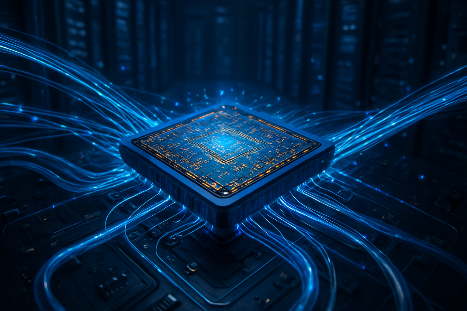
As of early 2026, the artificial intelligence industry has reached a critical inflection point where generic hardware is no longer enough to satisfy the hunger of multi-trillion parameter models. Leading this fundamental shift is Broadcom Inc. (NASDAQ: AVGO), which has successfully transitioned from a diversified networking giant into the primary architect of the custom AI silicon era. By positioning itself as the indispensable partner for hyperscalers like Google and Meta, and now the primary engine behind OpenAI’s hardware ambitions, Broadcom is witnessing a historic surge in revenue that is reshaping the semiconductor market.
The numbers tell a story of rapid, unprecedented dominance. After closing a blockbuster fiscal year 2025 with $20 billion in AI-related revenue, Broadcom is now on track to more than double that figure in 2026, with projections soaring toward the $50 billion mark. With an AI order backlog currently sitting at a staggering $73 billion, the company has effectively bifurcated the AI chip market: while Nvidia Corp. (NASDAQ: NVDA) remains the king of general-purpose training, Broadcom has become the undisputed sovereign of custom Application-Specific Integrated Circuits (ASICs), providing the "bespoke compute" that allows the world’s largest tech companies to bypass the "Nvidia tax" and build more efficient, specialized data centers.
Engineering the Architecture of Sovereign AI
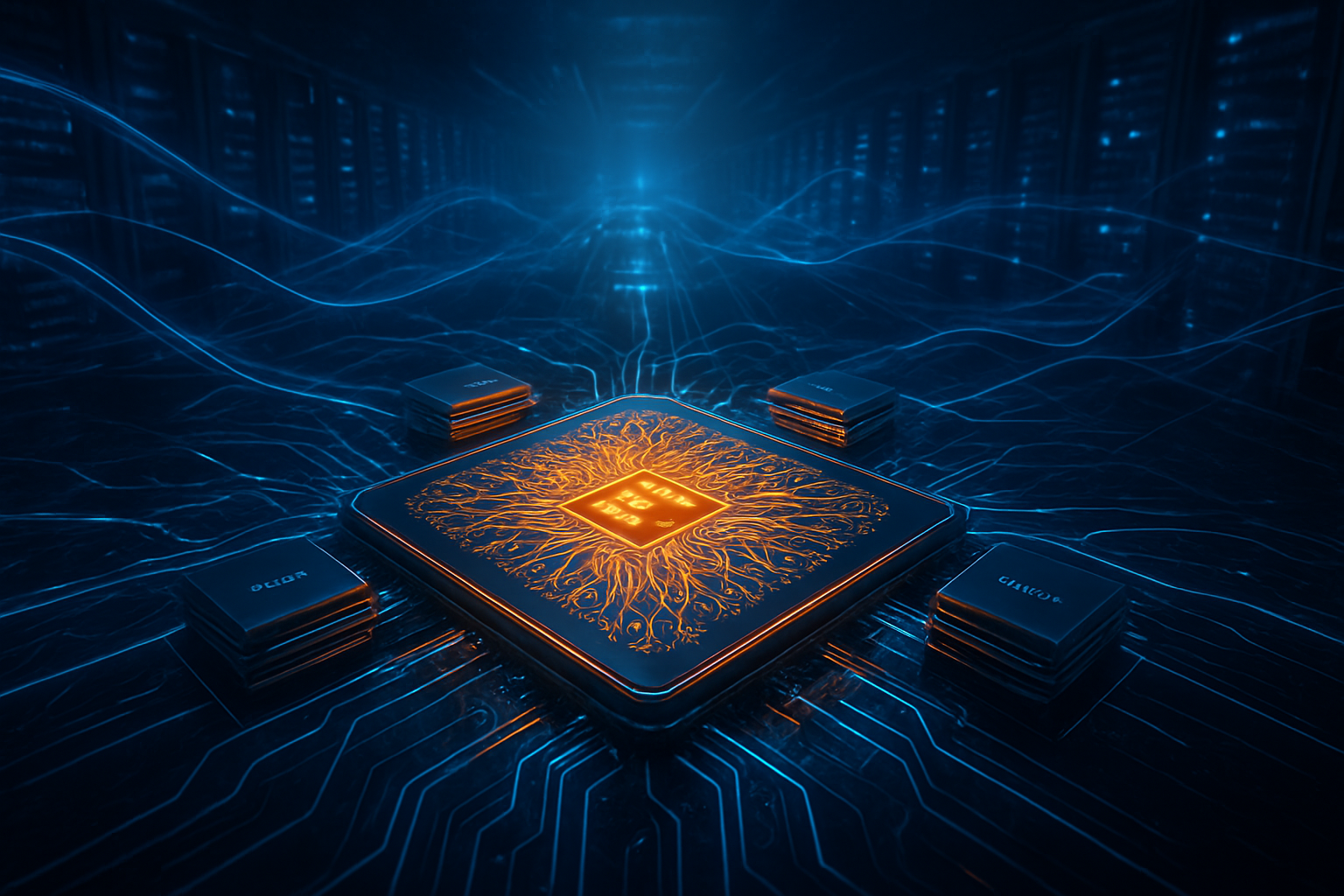
The core of Broadcom’s technical advantage lies in its ability to co-design chips that strip away the silicon "cruft" found in general-purpose GPUs. While Nvidia’s Blackwell and newly released Rubin platforms must support a vast array of legacy applications and diverse workloads, Broadcom’s ASICs—such as Google’s (NASDAQ: GOOGL) TPU v7 and Meta Platforms' (NASDAQ: META) MTIA v4—are laser-focused on the specific mathematical operations required for Large Language Models (LLMs). This specialization allows for a 30% to 50% improvement in performance-per-watt compared to off-the-shelf GPUs. In an era where data center power limits have become the primary bottleneck for AI scaling, this energy efficiency is not just a cost-saving measure; it is a strategic necessity.
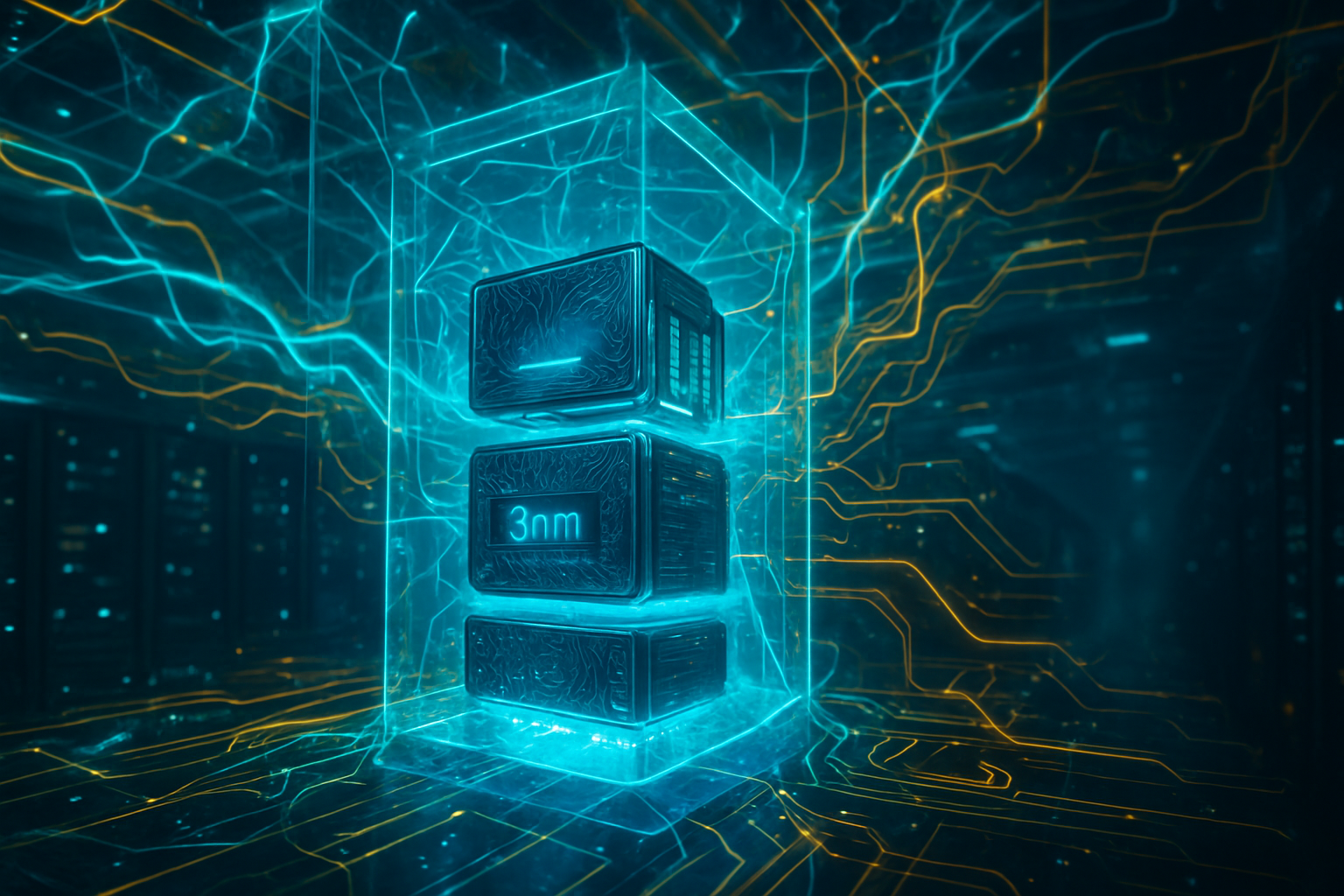
The technical specifications of these new accelerators are formidable. The Google TPU v7 (codenamed "Ironwood"), built on a 3nm process, is optimized specifically for the latest Gemini 2.0 and 3.0 models. Meanwhile, the Meta MTIA v4 (Santa Barbara), currently deploying across Meta’s massive fleet of servers, features liquid-cooled rack integration and advanced 3D Torus networking topologies. This architecture allows companies to cluster over 9,000 chips into a single unified "Superpod" with minimal latency, far exceeding the scale of traditional GPU clusters. Broadcom provides the critical intellectual property—including high-speed SerDes, HBM controllers, and networking interconnects—while leveraging its deep partnership with Taiwan Semiconductor Manufacturing Co. (NYSE: TSM) for advanced packaging.
Shifting the Competitive Power Balance
This surge in custom silicon is fundamentally altering the power dynamics among tech giants. By developing their own chips through Broadcom, companies like Meta and Google are achieving a level of vertical integration that provides a significant competitive moat. For these hyperscalers, the shift to ASICs represents a "decoupling" from the supply chain volatility and high margins associated with third-party GPU vendors. It allows them to optimize their entire stack—from the underlying silicon and networking to the AI models themselves—resulting in a lower Total Cost of Ownership (TCO) that startups and smaller labs simply cannot match.
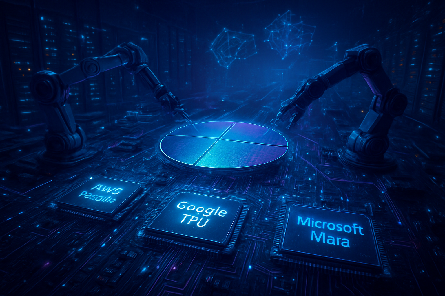
The market is also witnessing the emergence of a "second tier" of custom silicon providers, most notably Marvell Technology Inc. (NASDAQ: MRVL), which has secured its own landmark deals with Amazon and Microsoft. However, Broadcom remains the dominant force, controlling roughly 65% of the custom AI ASIC market. This positioning has made Broadcom a "proxy" for the overall health of the AI infrastructure sector. As OpenAI officially joins Broadcom’s customer roster with a multi-billion dollar project to build its own "sovereignty" chip, the company’s role has evolved from a supplier to a strategic kingmaker. OpenAI’s move to internal silicon, specifically designed to run its high-intensity "reasoning" models like the o1-series, signals that the industry's heaviest hitters are no longer content with being customers—they want to be architects.
The Broader Implications for the AI Landscape
Broadcom’s success reflects a broader trend toward the fragmentation of the AI hardware landscape. We are moving away from a world of "one size fits all" compute and toward a heterogeneous environment where different chips are tuned for specific tasks: training, inference, or reasoning. This shift mimics the evolution of the mobile industry, where Apple’s move to internal silicon eventually redefined the performance benchmarks for the entire smartphone market. By enabling Google, Meta, and OpenAI to do the same for AI, Broadcom is accelerating a future where the most advanced AI capabilities are tied directly to proprietary hardware.
However, this trend toward custom silicon also raises concerns about market consolidation. As the barrier to entry for high-end AI moves from "buying GPUs" to "designing multi-billion dollar custom chips," the gap between the "Big Five" hyperscalers and the rest of the industry may become an unbridgeable chasm. Furthermore, the reliance on a few key players—specifically Broadcom for design and TSMC for fabrication—creates new points of failure in the global AI supply chain. The environmental impact is also a double-edged sword; while ASICs are more efficient per operation, the sheer scale of the new data centers being built to house them is driving global energy demand to unprecedented heights.
The Horizon: 2nm Nodes and Reasoning-Specific Silicon
Looking toward 2027 and beyond, the roadmap for custom silicon is focused on the transition to 2nm-class nodes and the integration of even more advanced "Chip-on-Wafer-on-Substrate" (CoWoS) packaging. Broadcom is already in the early stages of development for the TPU v8, which is expected to begin mass production in the second half of 2026. These next-generation chips will likely incorporate on-chip optical interconnects, further reducing the latency and energy costs associated with moving data between processors and memory—a critical requirement for the next generation of "Agentic AI" that must process information in real-time.
Experts predict that the next major frontier will be the development of silicon specifically optimized for "reasoning-heavy" inference. Current chips are largely designed for the "next-token prediction" paradigm of GPT-4. However, as models move toward more complex chain-of-thought processing, the demand for chips with significantly higher local memory bandwidth and specialized logic for logic-gate simulation will grow. Broadcom’s partnership with OpenAI is widely believed to be the first major step in this direction, potentially creating a new category of "Reasoning Units" that differ fundamentally from current NPUs and GPUs.
Conclusion: A Legacy Defined by Customization
Broadcom’s transformation into an AI silicon powerhouse is one of the most significant developments in the history of the semiconductor industry. By 2026, the company has proven that the path to AI supremacy is paved with customization, not just raw power. Its $50 billion revenue surge is a testament to the fact that for the world’s most advanced AI labs, the "off-the-shelf" era is effectively over. Broadcom’s ability to turn the complex requirements of companies like Google, Meta, and OpenAI into physical, high-performance silicon has placed it at the center of the AI ecosystem.
In the coming months, the industry will be watching closely as the first "live silicon" from the OpenAI-Broadcom partnership begins to ship. This event will likely serve as a litmus test for whether internal silicon can truly provide the "sovereignty" that AI labs crave. For investors and technologists alike, Broadcom is no longer just a networking company; it is the master builder of the infrastructure that will define the next decade of artificial intelligence.
This content is intended for informational purposes only and represents analysis of current AI developments.
TokenRing AI delivers enterprise-grade solutions for multi-agent AI workflow orchestration, AI-powered development tools, and seamless remote collaboration platforms.
For more information, visit https://www.tokenring.ai/.