Tag: Google TPU

  • The Great Silicon Squeeze: Why Google and Microsoft are Sacrificing Billions to Break the HBM and CoWoS Bottleneck

    The Great Silicon Squeeze: Why Google and Microsoft are Sacrificing Billions to Break the HBM and CoWoS Bottleneck

    As of January 2026, the artificial intelligence industry has reached a fever pitch, not just in the complexity of its models, but in the physical reality of the hardware required to run them. The "compute crunch" of 2024 and 2025 has evolved into a structural "capacity wall" centered on two critical components: High Bandwidth Memory (HBM) and Chip-on-Wafer-on-Substrate (CoWoS) advanced packaging. For industry titans like Google (NASDAQ:GOOGL) and Microsoft (NASDAQ:MSFT), the strategy has shifted from optimizing the Total Cost of Ownership (TCO) to an aggressive, almost desperate, pursuit of Time-to-Market (TTM). In the race for Artificial General Intelligence (AGI), these giants have signaled that they are willing to pay any price to cut the manufacturing queue, effectively prioritizing speed over cost in a high-stakes scramble for silicon.

    The immediate significance of this shift cannot be overstated. By January 2026, the demand for CoWoS packaging has surged to nearly one million wafers per year, far outstripping the aggressive expansion efforts of TSMC (NYSE:TSM). This bottleneck has created a "vampire effect," where the production of AI accelerators is siphoning resources away from the broader electronics market, leading to rising costs for everything from smartphones to automotive chips. For Google and Microsoft, securing these components is no longer just a procurement task—it is a matter of corporate survival and geopolitical leverage.

    The Technical Frontier: HBM4 and the 16-Hi Arms Race

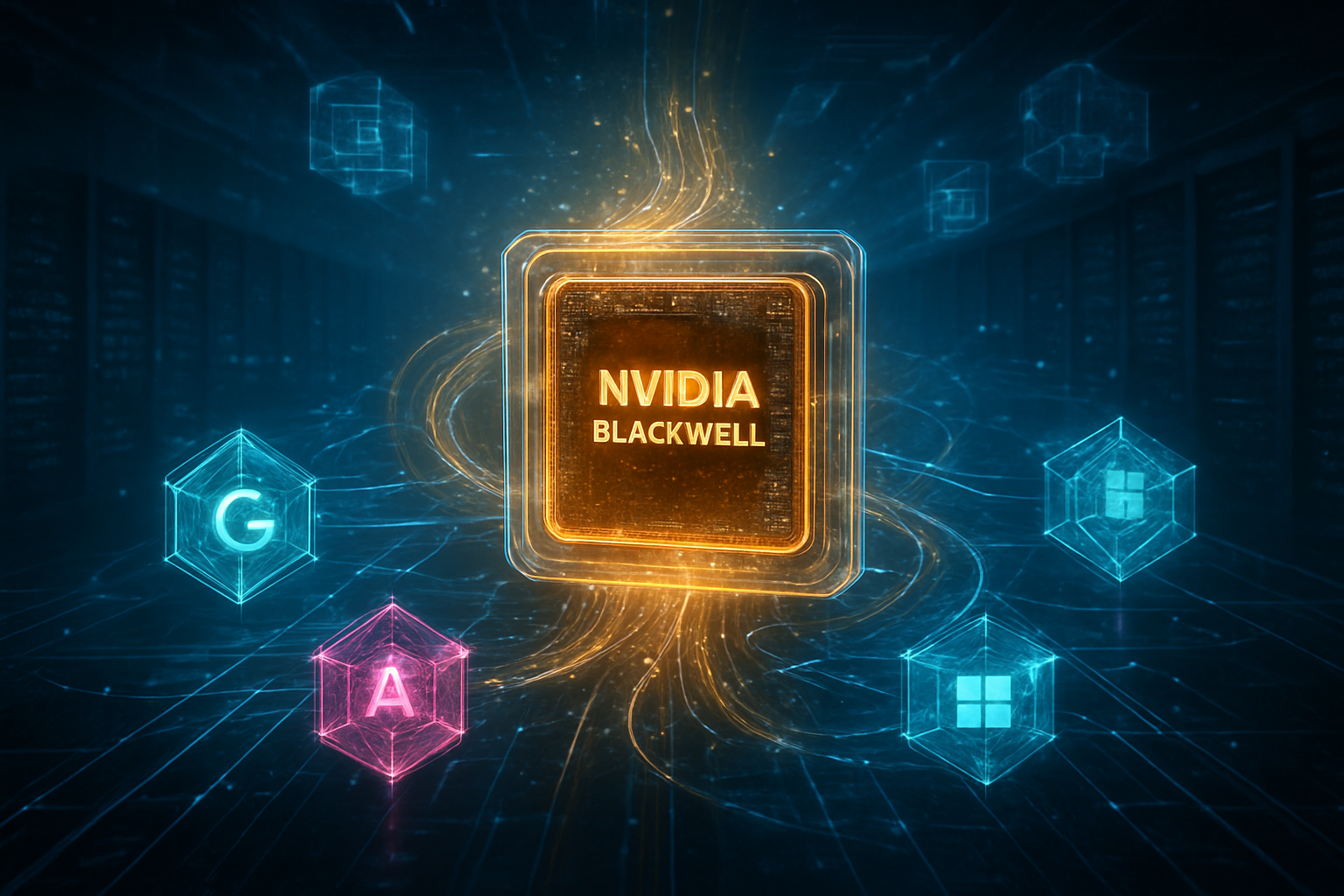
    At the heart of the current bottleneck is the transition from HBM3e to the next-generation HBM4 standard. While HBM3e was sufficient for the initial waves of Large Language Models (LLMs), the massive parameter counts of 2026-era models require the 2048-bit memory interface width offered by HBM4—a doubling of the 1024-bit interface used in previous generations. This technical leap is essential for feeding the voracious data appetites of chips like NVIDIA’s (NASDAQ:NVDA) new Rubin architecture and Google’s TPU v7, codenamed "Ironwood."

    The engineering challenge of HBM4 lies in the physical stacking of memory. The industry is currently locked in a "16-Hi arms race," where 16 layers of DRAM are stacked into a single package. To keep these stacks within the JEDEC-defined thickness of 775 micrometers, manufacturers like SK Hynix (KRX:000660) and Samsung (KRX:005930) have had to reduce wafer thickness to a staggering 30 micrometers. This thinning process has cratered yields and necessitated a shift toward "Hybrid Bonding"—a copper-to-copper connection method that replaces traditional micro-bumps. This complexity is exactly why CoWoS (Chip-on-Wafer-on-Substrate) has become the primary point of failure in the supply chain; it is the specialized "glue" that connects these ultra-thin memory stacks to the logic processors.

    Initial reactions from the research community suggest that while HBM4 provides the necessary bandwidth to avoid "memory wall" stalls, the thermal dissipation issues are becoming a nightmare for data center architects. Industry experts note that the move to 16-Hi stacks has forced a redesign of cooling systems, with liquid-to-chip cooling now becoming a mandatory requirement for any Tier-1 AI cluster. This technical hurdle has only increased the reliance on TSMC’s advanced CoWoS-L (Local Silicon Interconnect) packaging, which remains the only viable solution for the high-density interconnects required by the latest Blackwell Ultra and Rubin platforms.

    Strategic Maneuvers: Custom Silicon vs. The NVIDIA Tax

    The strategic landscape of 2026 is defined by a "dual-track" approach from the hyperscalers. Microsoft and Google are simultaneously NVIDIA’s largest customers and its most formidable competitors. Microsoft (NASDAQ:MSFT) has accelerated the mass production of its Maia 200 (Braga) accelerator, while Google has moved aggressively with its TPU v7 fleet. The goal is simple: reduce the "NVIDIA tax," which currently sees NVIDIA command gross margins north of 75% on its high-end H100 and B200 systems.

    However, building custom silicon does not exempt these companies from the HBM and CoWoS bottleneck. Even a custom-designed TPU requires the same HBM4 stacks and the same TSMC packaging slots as an NVIDIA Rubin chip. To secure these, Google has leveraged its long-standing partnership with Broadcom (NASDAQ:AVGO) to lock in nearly 50% of Samsung’s 2026 HBM4 production. Meanwhile, Microsoft has turned to Marvell (NASDAQ:MRVL) to help reserve dedicated CoWoS-L capacity at TSMC’s new AP8 facility in Taiwan. By paying massive prepayments—estimated in the billions of dollars—these companies are effectively "buying the queue," ensuring that their internal projects aren't sidelined by NVIDIA’s overwhelming demand.

    The competitive implications are stark. Startups and second-tier cloud providers are increasingly being squeezed out of the market. While a company like CoreWeave or Lambda can still source NVIDIA GPUs, they lack the vertical integration and the capital to secure the raw components (HBM and CoWoS) at the source. This has allowed Google and Microsoft to maintain a strategic advantage: even if they can't build a better chip than NVIDIA, they can ensure they have more chips, and have them sooner, by controlling the underlying supply chain.

    The Global AI Landscape: The "Vampire Effect" and Sovereign AI

    The scramble for HBM and CoWoS is having a profound impact on the wider technology landscape. Economists have noted a "Vampire Effect," where the high margins of AI memory are causing manufacturers like Micron (NASDAQ:MU) and SK Hynix to convert standard DDR4 and DDR5 production lines into HBM lines. This has led to an unexpected 20% price hike in "boring" memory for PCs and servers, as the supply of commodity DRAM shrinks to feed the AI beast. The AI bottleneck is no longer a localized issue; it is a macroeconomic force driving inflation across the semiconductor sector.

    Furthermore, the emergence of "Sovereign AI" has added a new layer of complexity. Nations like the UAE, France, and Japan have begun treating AI compute as a national utility, similar to energy or water. These governments are reportedly paying "sovereign premiums" to secure turnkey NVIDIA Rubin NVL144 racks, further inflating the price of the limited CoWoS capacity. This geopolitical dimension means that Google and Microsoft are not just competing against each other, but against national treasuries that view AI leadership as a matter of national security.

    This era of "Speed over Cost" marks a significant departure from previous tech cycles. In the mobile or cloud eras, companies prioritized efficiency and cost-per-user. In the AGI race of 2026, the consensus is that being six months late with a frontier model is a multi-billion dollar failure that no amount of cost-saving can offset. This has led to a "Capex Cliff," where investors are beginning to demand proof of ROI, yet companies feel they cannot afford to stop spending lest they fall behind permanently.

    Future Outlook: Glass Substrates and the Post-CoWoS Era

    Looking toward the end of 2026 and into 2027, the industry is already searching for a way out of the CoWoS trap. One of the most anticipated developments is the shift toward glass substrates. Unlike the organic materials currently used in packaging, glass offers superior flatness and thermal stability, which could allow for even denser interconnects and larger "system-on-package" designs. Intel (NASDAQ:INTC) and several South Korean firms are racing to commercialize this technology, which could finally break TSMC’s "secondary monopoly" on advanced packaging.

    Additionally, the transition to HBM4 will likely see the integration of the "logic die" directly into the memory stack, a move that will require even closer collaboration between memory makers and foundries. Experts predict that by 2027, the distinction between a "memory company" and a "foundry" will continue to blur, as SK Hynix and Samsung begin to incorporate TSMC-manufactured logic into their HBM stacks. The challenge will remain one of yield; as the complexity of these 3D-stacked systems increases, the risk of a single defect ruining a $50,000 chip becomes a major financial liability.

    Summary of the Silicon Scramble

    The HBM and CoWoS bottleneck of 2026 represents a pivotal moment in the history of computing. It is the point where the abstract ambitions of AI software have finally collided with the hard physical limits of material science and manufacturing capacity. Google and Microsoft's decision to prioritize speed over cost is a rational response to a market where "time-to-intelligence" is the only metric that matters. By locking down the supply of HBM4 and CoWoS, they are not just building data centers; they are fortifying their positions in the most expensive arms race in human history.

    In the coming months, the industry will be watching for the first production yields of 16-Hi HBM4 and the operational status of TSMC’s Arizona packaging plants. If these facilities can hit their targets, the bottleneck may begin to ease by late 2027. However, if yields remain low, the "Speed over Cost" era may become the permanent state of the AI industry, favoring only those with the deepest pockets and the most aggressive supply chain strategies. For now, the silicon squeeze continues, and the price of entry into the AI elite has never been higher.


    This content is intended for informational purposes only and represents analysis of current AI developments.

    TokenRing AI delivers enterprise-grade solutions for multi-agent AI workflow orchestration, AI-powered development tools, and seamless remote collaboration platforms.
    For more information, visit https://www.tokenring.ai/.

  • The Blackwell Era: Nvidia’s GB200 NVL72 Redefines the Trillion-Parameter Frontier

    The Blackwell Era: Nvidia’s GB200 NVL72 Redefines the Trillion-Parameter Frontier

    As of January 1, 2026, the artificial intelligence landscape has reached a pivotal inflection point, transitioning from the frantic "training race" of previous years to a sophisticated era of massive, real-time inference. At the heart of this shift is the full-scale deployment of Nvidia’s (NASDAQ:NVDA) Blackwell architecture, specifically the GB200 NVL72 liquid-cooled racks. These systems, now shipping at a rate of approximately 1,000 units per week, have effectively reset the benchmarks for what is possible in generative AI, enabling the seamless operation of trillion-parameter models that were once considered computationally prohibitive for widespread use.

    The arrival of the Blackwell era marks a fundamental change in the economics of intelligence. With a staggering 25x reduction in the total cost of ownership (TCO) for inference and a similar leap in energy efficiency, Nvidia has transformed the AI data center into a high-output "AI factory." However, this dominance is facing its most significant challenge yet as hyperscalers like Alphabet (NASDAQ:GOOGL) and Meta (NASDAQ:META) accelerate their own custom silicon programs. The battle for the future of AI compute is no longer just about raw power; it is about the efficiency of every token generated and the strategic autonomy of the world’s largest tech giants.

    The Technical Architecture of the Blackwell Superchip

    The GB200 NVL72 is not merely a collection of GPUs; it is a singular, massive compute engine. Each rack integrates 72 Blackwell GPUs and 36 Grace CPUs, interconnected via the fifth-generation NVLink, which provides a staggering 1.8 TB/s of bidirectional throughput per GPU. This allows the entire rack to act as a single GPU with 1.4 exaflops of AI performance and 30 TB of fast memory. The shift to the Blackwell Ultra (B300) variant in late 2025 further expanded this capability, introducing 288GB of HBM3E memory per chip to accommodate the massive context windows required by 2026’s "reasoning" models, such as OpenAI’s latest o-series and DeepSeek’s R-1 successors.

    Technically, the most significant advancement lies in the second-generation Transformer Engine, which utilizes micro-scaling formats including 4-bit floating point (FP4) precision. This allows Blackwell to deliver 30x the inference performance for 1.8-trillion parameter models compared to the previous H100 generation. Furthermore, the transition to liquid cooling has become a necessity rather than an option. With the TDP of individual B200 chips exceeding 1200W, the GB200 NVL72’s liquid-cooling manifold is the only way to maintain the thermal efficiency required for sustained high-load operations. This architectural shift has forced a massive global overhaul of data center infrastructure, as traditional air-cooled facilities are rapidly being retrofitted or replaced to support the high-density requirements of the Blackwell era.

    Industry experts have been quick to note that while the raw TFLOPS are impressive, the real breakthrough is the reduction in "communication tax." By utilizing the NVLink Switch System, Blackwell minimizes the latency typically associated with moving data between chips. Initial reactions from the research community emphasize that this allows for a "reasoning-at-scale" capability, where models can perform thousands of internal "thoughts" or steps before outputting a final answer to a user, all while maintaining a low-latency experience. This hardware breakthrough has effectively ended the era of "dumb" chatbots, ushering in an era of agentic AI that can solve complex multi-step problems in seconds.

    Competitive Pressure and the Rise of Custom Silicon

    While Nvidia (NASDAQ:NVDA) currently maintains an estimated 85-90% share of the merchant AI silicon market, the competitive landscape in 2026 is increasingly defined by "custom-built" alternatives. Alphabet (NASDAQ:GOOGL) has successfully deployed its seventh-generation TPU, codenamed "Ironwood" (TPU v7). These chips are designed specifically for the JAX and XLA software ecosystems, offering a compelling alternative for large-scale developers like Anthropic. Ironwood pods support up to 9,216 chips in a single synchronous configuration, matching Blackwell’s memory bandwidth and providing a more cost-effective solution for Google Cloud customers who don't require the broad compatibility of Nvidia’s CUDA platform.

    Meta (NASDAQ:META) has also made significant strides with its third-generation Meta Training and Inference Accelerator (MTIA 3). Unlike Nvidia’s general-purpose approach, MTIA 3 is surgically optimized for Meta’s internal recommendation and ranking algorithms. By January 2026, MTIA now handles over 50% of the internal workloads for Facebook and Instagram, significantly reducing Meta’s reliance on external silicon for its core business. This strategic move allows Meta to reserve its massive Blackwell clusters exclusively for the pre-training of its next-generation Llama frontier models, effectively creating a tiered hardware strategy that maximizes both performance and cost-efficiency.

    This surge in custom ASICs (Application-Specific Integrated Circuits) is creating a two-tier market. On one side, Nvidia remains the "gold standard" for frontier model training and general-purpose AI services used by startups and enterprises. On the other, hyperscalers like Amazon (NASDAQ:AMZN) and Microsoft (NASDAQ:MSFT) are aggressively pushing their own chips—Trainium/Inferentia and Maia, respectively—to lock in customers and lower their own operational overhead. The competitive implication is clear: Nvidia can no longer rely solely on being the fastest; it must now leverage its deep software moat, including the TensorRT-LLM libraries and the CUDA ecosystem, to prevent customers from migrating to these increasingly capable custom alternatives.

    The Global Impact of the 25x TCO Revolution

    The broader significance of the Blackwell deployment lies in the democratization of high-end inference. Nvidia’s claim of a 25x reduction in total cost of ownership has been largely validated by production data in early 2026. For a cloud provider, the cost of generating a million tokens has plummeted by nearly 20x compared to the Hopper (H100) generation. This economic shift has turned AI from an expensive experimental cost center into a high-margin utility. It has enabled the rise of "AI Factories"—massive data centers dedicated entirely to the production of intelligence—where the primary metric of success is no longer uptime, but "tokens per watt."

    However, this rapid advancement has also raised significant concerns regarding energy consumption and the "digital divide." While Blackwell is significantly more efficient per token, the sheer scale of deployment means that the total energy demand of the AI sector continues to climb. Companies like Oracle (NYSE:ORCL) have responded by co-locating Blackwell clusters with modular nuclear reactors (SMRs) to ensure a stable, carbon-neutral power supply. This trend highlights a new reality where AI hardware development is inextricably linked to national energy policy and global sustainability goals.

    Furthermore, the Blackwell era has redefined the "Memory Wall." As models grow to include trillions of parameters and context windows that span millions of tokens, the ability of hardware to keep that data "hot" in memory has become the primary bottleneck. Blackwell’s integration of high-bandwidth memory (HBM3E) and its massive NVLink fabric represent a successful, albeit expensive, solution to this problem. It sets a new standard for the industry, suggesting that future breakthroughs in AI will be as much about data movement and thermal management as they are about the underlying silicon logic.

    Looking Ahead: The Road to Rubin and AGI

    As we look toward the remainder of 2026, the industry is already anticipating Nvidia’s next move: the Rubin architecture (R100). Expected to enter mass production in the second half of the year, Rubin is rumored to feature HBM4 and an even more advanced 4×4 mesh interconnect. The near-term focus will be on further integrating AI hardware with "physical AI" applications, such as humanoid robotics and autonomous manufacturing, where the low-latency inference capabilities of Blackwell are already being put to the test.

    The primary challenge moving forward will be the transition from "static" models to "continuously learning" systems. Current hardware is optimized for fixed weights, but the next generation of AI will likely require chips that can update their knowledge in real-time without massive retraining costs. Experts predict that the hardware of 2027 and beyond will need to incorporate more neuromorphic or "brain-like" architectures to achieve the next order-of-magnitude leap in efficiency.

    In the long term, the success of Blackwell and its successors will be measured by their ability to support the pursuit of Artificial General Intelligence (AGI). As models move beyond simple text and image generation into complex reasoning and scientific discovery, the hardware must evolve to support non-linear thought processes. The GB200 NVL72 is the first step toward this "reasoning" infrastructure, providing the raw compute needed for models to simulate millions of potential outcomes before making a decision.

    Summary: A Landmark in AI History

    The deployment of Nvidia’s Blackwell GPUs and GB200 NVL72 racks stands as one of the most significant milestones in the history of computing. By delivering a 25x reduction in TCO and 30x gains in inference performance, Nvidia has effectively ended the era of "AI scarcity." Intelligence is now becoming a cheap, abundant commodity, fueling a new wave of innovation across every sector of the global economy. While custom silicon from Google and Meta provides a necessary competitive check, the Blackwell architecture remains the benchmark against which all other AI hardware is measured.

    As we move further into 2026, the key takeaways are clear: the "moat" in AI has shifted from training to inference efficiency, liquid cooling is the new standard for data center design, and the integration of hardware and software is more critical than ever. The industry has moved past the hype of the early 2020s and into a phase of industrial-scale execution. For investors and technologists alike, the coming months will be defined by how effectively these massive Blackwell clusters are utilized to solve real-world problems, from climate modeling to drug discovery.

    The "AI supercycle" is no longer a prediction—it is a reality, powered by the most complex and capable machines ever built. All eyes now remain on the production ramps of the late-2026 Rubin architecture and the continued evolution of custom silicon, as the race to build the foundation of the next intelligence age continues unabated.


    This content is intended for informational purposes only and represents analysis of current AI developments.

    TokenRing AI delivers enterprise-grade solutions for multi-agent AI workflow orchestration, AI-powered development tools, and seamless remote collaboration platforms.
    For more information, visit https://www.tokenring.ai/.

  • The Great Decoupling: How Hyperscaler Custom Silicon is Ending NVIDIA’s AI Monopoly

    The Great Decoupling: How Hyperscaler Custom Silicon is Ending NVIDIA’s AI Monopoly

    The artificial intelligence industry has reached a historic inflection point as of early 2026, marking the beginning of what analysts call the "Great Decoupling." For years, the tech world was beholden to the supply chains and pricing power of NVIDIA Corporation (NASDAQ: NVDA), whose H100 and Blackwell GPUs became the de facto currency of the generative AI era. However, the tide has turned. As the industry shifts its focus from training massive foundation models to the high-volume, cost-sensitive world of inference, the world’s largest hyperscalers—Google, Amazon, and Meta—have finally unleashed their secret weapons: custom-built AI accelerators designed to bypass the "NVIDIA tax."

    Leading this charge is the general availability of Alphabet Inc.’s (NASDAQ: GOOGL) TPU v7, codenamed "Ironwood." Alongside the deployment of Amazon.com, Inc.’s (NASDAQ: AMZN) Trainium 3 and Meta Platforms, Inc.’s (NASDAQ: META) MTIA v3, these chips represent a fundamental shift in the AI power dynamic. No longer content to be just NVIDIA’s biggest customers, these tech giants are vertically integrating their hardware and software stacks to achieve "silicon sovereignty," promising to slash AI operating costs and redefine the competitive landscape for the next decade.

    The Ironwood Era: Inside Google’s TPU v7 Breakthrough

    Google’s TPU v7 "Ironwood," which entered general availability in late 2025, represents the most significant architectural overhaul in the Tensor Processing Unit's decade-long history. Built on a cutting-edge 3nm process node, Ironwood delivers a staggering 4.6 PFLOPS of dense FP8 compute per chip—an 11x increase over the TPU v5p. More importantly, it features 192GB of HBM3e memory with a bandwidth of 7.4 TB/s, specifically engineered to handle the massive KV-caches required for the latest trillion-parameter frontier models like Gemini 2.0 and the upcoming Gemini 3.0.

    What truly sets Ironwood apart from NVIDIA’s Blackwell architecture is its networking philosophy. While NVIDIA relies on NVLink to cluster GPUs in relatively small pods, Google has refined its proprietary Optical Circuit Switch (OCS) and 3D Torus topology. A single Ironwood "Superpod" can connect 9,216 chips into a unified compute domain, providing an aggregate of 42.5 ExaFLOPS of FP8 compute. This allows Google to treat thousands of chips as a single "brain," drastically reducing the latency and networking overhead that typically plagues large-scale distributed inference.

    Initial reactions from the AI research community have been overwhelmingly positive, particularly regarding the TPU’s energy efficiency. Experts at the AI Hardware Summit noted that while NVIDIA’s B200 remains a powerhouse for raw training, Ironwood offers nearly double the performance-per-watt for inference tasks. This efficiency is a direct result of Google’s ASIC approach: by stripping away the legacy graphics circuitry found in general-purpose GPUs, Google has created a "lean and mean" machine dedicated solely to the matrix multiplications that power modern transformers.

    The Cloud Counter-Strike: AWS and Meta’s Silicon Sovereignty

    Not to be outdone, Amazon.com, Inc. (NASDAQ: AMZN) has accelerated its custom silicon roadmap with the full deployment of Trainium 3 (Trn3) in early 2026. Manufactured on TSMC’s 3nm node, Trn3 marks a strategic pivot for AWS: the convergence of its training and inference lines. Amazon has realized that the "thinking" models of 2026, such as Anthropic’s Claude 4 and Amazon’s own Nova series, require the massive memory and FLOPS previously reserved for training. Trn3 delivers 2.52 PFLOPS of FP8 compute, offering a 50% better price-performance ratio than the equivalent NVIDIA H100 or B200 instances currently available on the market.

    Meta Platforms, Inc. (NASDAQ: META) is also making massive strides with its MTIA v3 (Meta Training and Inference Accelerator). While Meta remains one of NVIDIA’s largest customers for the raw training of its Llama family, the company has begun migrating its massive recommendation engines—the heart of Facebook and Instagram—to its own silicon. MTIA v3 features a significant upgrade to HBM3e memory, allowing Meta to serve Llama 4 models to billions of users with a fraction of the power consumption required by off-the-shelf GPUs. This move toward infrastructure autonomy is expected to save Meta billions in capital expenditures over the next three years.

    Even Microsoft Corporation (NASDAQ: MSFT) has joined the fray with the volume rollout of its Maia 200 (Braga) chips. Designed to reduce the "Copilot tax" for Azure OpenAI services, Maia 200 is now powering a significant portion of ChatGPT’s inference workloads. This collective push by the hyperscalers has created a multi-polar hardware ecosystem where the choice of chip is increasingly dictated by the specific model architecture and the desired cost-per-token, rather than brand loyalty to NVIDIA.

    Breaking the CUDA Moat: The Software Revolution

    The primary barrier to decoupling has always been NVIDIA’s proprietary CUDA software ecosystem. However, in 2026, that moat is being bridged by a maturing open-source software stack. OpenAI’s Triton has emerged as the industry’s primary "off-ramp," allowing developers to write high-performance kernels in Python that are hardware-agnostic. Triton now features mature backends for Google’s TPU, AWS Trainium, and even AMD’s MI350 series, effectively neutralizing the software advantage that once made NVIDIA GPUs indispensable.

    Furthermore, the integration of PyTorch 2.x and the upcoming 3.0 release has solidified torch.compile as the standard for AI development. By using the OpenXLA (Accelerated Linear Algebra) compiler and the PJRT interface, PyTorch can now automatically optimize models for different hardware backends with minimal performance loss. This means a developer can train a model on an NVIDIA-based workstation and deploy it to a Google TPU v7 or an AWS Trainium 3 cluster with just a few lines of code.

    This software abstraction has profound implications for the market. It allows AI labs and startups to build "Agentlakes"—composable architectures that can dynamically shift workloads between different cloud providers based on real-time pricing and availability. The "NVIDIA tax"—the 70-80% margins the company once commanded—is being eroded as hyperscalers use their own silicon to offer AI services at lower price points, forcing a competitive race to the bottom in the inference market.

    The Future of Distributed Compute: 2nm and Beyond

    Looking ahead to late 2026 and 2027, the battle for silicon supremacy will move to the 2nm process node. Industry insiders predict that the next generation of chips will focus heavily on "Interconnect Fusion." NVIDIA is already fighting back with its NVLink Fusion technology, which aims to open its high-speed interconnects to third-party ASICs, attempting to move the lock-in from the chip level to the network level. Meanwhile, Google is rumored to be working on TPU v8, which may feature integrated photonic interconnects directly on the die to eliminate electronic bottlenecks entirely.

    The next frontier will also involve "Edge-to-Cloud" continuity. As models become more modular through techniques like Mixture-of-Experts (MoE), we expect to see hybrid inference strategies where the "base" of a model runs on energy-efficient custom silicon in the cloud, while specialized "expert" modules run locally on 2nm-powered mobile devices and PCs. This would create a truly distributed AI fabric, further reducing the reliance on massive centralized GPU clusters.

    However, challenges remain. The fragmentation of the hardware landscape could lead to a "optimization tax," where developers spend more time tuning models for different architectures than they do on actual research. Additionally, the massive capital requirements for 2nm fabrication mean that only the largest hyperscalers can afford to play this game, potentially leading to a new form of "Cloud Oligarchy" where smaller players are priced out of the custom silicon race.

    Conclusion: A New Era of AI Economics

    The "Great Decoupling" of 2026 marks the end of the monolithic GPU era and the birth of a more diverse, efficient, and competitive AI hardware ecosystem. While NVIDIA remains a dominant force in high-end research and frontier model training, the rise of Google’s TPU v7 Ironwood, AWS Trainium 3, and Meta’s MTIA v3 has proven that the world’s biggest tech companies are no longer willing to outsource their infrastructure's future.

    The key takeaway for the industry is that AI is transitioning from a scarcity-driven "gold rush" to a cost-driven "utility phase." In this new world, "Silicon Sovereignty" is the ultimate strategic advantage. As we move into the second half of 2026, the industry will be watching closely to see how NVIDIA responds to this erosion of its moat and whether the open-source software stack can truly maintain parity across such a diverse range of hardware. One thing is certain: the era of the $40,000 general-purpose GPU as the only path to AI success is officially over.


    This content is intended for informational purposes only and represents analysis of current AI developments.

    TokenRing AI delivers enterprise-grade solutions for multi-agent AI workflow orchestration, AI-powered development tools, and seamless remote collaboration platforms.
    For more information, visit https://www.tokenring.ai/.

  • Hyperscalers Accelerate Custom Silicon Deployment to Challenge NVIDIA’s AI Dominance

    Hyperscalers Accelerate Custom Silicon Deployment to Challenge NVIDIA’s AI Dominance

    The artificial intelligence hardware landscape is undergoing a seismic shift, characterized by industry analysts as the "Great Decoupling." As of late 2025, the world’s largest cloud providers—Alphabet Inc. (NASDAQ: GOOGL), Amazon.com Inc. (NASDAQ: AMZN), and Meta Platforms Inc. (NASDAQ: META)—have reached a critical mass in their efforts to reduce reliance on NVIDIA (NASDAQ: NVDA). This movement is no longer a series of experimental projects but a full-scale industrial pivot toward custom Application-Specific Integrated Circuits (ASICs) designed to optimize performance and bypass the high premiums associated with third-party hardware.

    The immediate significance of this shift is most visible in the high-volume inference market, where custom silicon now captures nearly 40% of all workloads. By deploying their own chips, these hyperscalers are effectively avoiding the "NVIDIA tax"—the 70% to 80% gross margins commanded by the market leader—while simultaneously tailoring their hardware to the specific needs of their massive software ecosystems. While NVIDIA remains the undisputed champion of frontier model training, the rise of specialized silicon for inference marks a new era of cost-efficiency and architectural sovereignty for the tech giants.

    Silicon Sovereignty: The Specs Behind the Shift

    The technical vanguard of this movement is led by Google’s seventh-generation Tensor Processing Unit, codenamed TPU v7 'Ironwood.' Unveiled with staggering specifications, Ironwood claims a performance of 4.6 PetaFLOPS of dense FP8 compute per chip. This puts it in a dead heat with NVIDIA’s Blackwell B200 architecture. Beyond raw speed, Google has optimized Ironwood for massive scale, utilizing an Optical Circuit Switch (OCS) fabric that allows the company to link 9,216 chips into a single "Superpod" with nearly 2 Petabytes of shared memory. This architecture is specifically designed to handle the trillion-parameter models that define the current state of generative AI.

    Not to be outdone, Amazon has scaled its Trainium3 and Inferentia lines, moving to a unified 3nm process for its latest silicon. The Trainium3 UltraServer integrates 144 chips per rack to aggregate 362 FP8 PetaFLOPS, offering a 30% to 40% price-performance advantage over general-purpose GPUs for AWS customers. Meanwhile, Meta’s MTIA v2 (Artemis) has seen broad deployment across its global data center footprint. Unlike its competitors, Meta has prioritized a massive SRAM hierarchy over expensive High Bandwidth Memory (HBM) for its specific recommendation and ranking workloads, resulting in a 44% lower Total Cost of Ownership (TCO) compared to commercial alternatives.

    Industry experts note that this differs fundamentally from previous hardware cycles. In the past, general-purpose GPUs were necessary because AI algorithms were changing too rapidly for fixed-function ASICs to keep up. However, the maturation of the Transformer architecture and the standardization of data types like FP8 have allowed hyperscalers to "freeze" certain hardware requirements into silicon without the risk of immediate obsolescence.

    Competitive Implications for the AI Ecosystem

    The "Great Decoupling" is creating a bifurcated market that benefits the hyperscalers while forcing NVIDIA to accelerate its own innovation cycle. For Alphabet, Amazon, and Meta, the primary benefit is margin expansion. By "paying cost" for their own silicon rather than market prices, these companies can offer AI services at a price point that is difficult for smaller cloud competitors to match. This strategic advantage allows them to subsidize their AI research and development through hardware savings, creating a virtuous cycle of reinvestment.

    For NVIDIA, the challenge is significant but not yet existential. The company still maintains a 90% share of the frontier model training market, where flexibility and absolute peak performance are paramount. However, as inference—the process of running a trained model for users—becomes the dominant share of AI compute spending, NVIDIA is being pushed into a "premium tier" where it must justify its costs through superior software and networking. The erosion of the "CUDA Moat," driven by the rise of open-source compilers like OpenAI’s Triton and PyTorch 2.x, has made it significantly easier for developers to port their models to Google’s TPUs or Amazon’s Trainium without a massive engineering overhead.

    Startups and smaller AI labs stand to benefit from this competition as well. The availability of diversified hardware options in the cloud means that the "compute crunch" of 2023 and 2024 has largely eased. Companies can now choose hardware based on their specific needs: NVIDIA for cutting-edge research, and custom ASICs for cost-effective, large-scale deployment.

    The Economic and Strategic Significance

    The wider significance of this shift lies in the democratization of high-performance compute at the infrastructure level. We are moving away from a monolithic hardware era toward a specialized one. This fits into the broader trend of "vertical integration," where the software, the model, and the silicon are co-designed. When a company like Meta designs a chip specifically for its recommendation algorithms, it achieves efficiencies that a general-purpose chip simply cannot match, regardless of its raw power.

    However, this transition is not without concerns. The reliance on custom silicon could lead to "vendor lock-in" at the hardware level, where a model optimized for Google’s TPU v7 may not perform as well on Amazon’s Trainium3. Furthermore, the massive capital expenditure required to design and manufacture 3nm chips means that only the wealthiest companies can participate in this decoupling. This could potentially centralize AI power even further among the "Magnificent Seven" tech giants, as the cost of entry for custom silicon is measured in billions of dollars.

    Comparatively, this milestone is being likened to the transition from general-purpose CPUs to GPUs in the early 2010s. Just as the GPU unlocked the potential of deep learning, the custom ASIC is unlocking the potential of "AI at scale," making it economically viable to serve generative AI to billions of users simultaneously.

    Future Horizons: Beyond the 3nm Era

    Looking ahead, the next 24 to 36 months will see an even more aggressive roadmap. NVIDIA is already preparing its Rubin architecture, which is expected to debut in late 2026 with HBM4 memory and "Vera" CPUs, aiming to reclaim the performance lead. In response, hyperscalers are already in the design phase for their next-generation chips, focusing on "chiplet" architectures that allow for even more modular and scalable designs.

    We can expect to see more specialized use cases on the horizon, such as "edge ASICs" designed for local inference on mobile devices and IoT hardware, further extending the reach of these custom stacks. The primary challenge remains the supply chain; as everyone moves to 3nm and 2nm processes, the competition for manufacturing capacity at foundries like TSMC will be the ultimate bottleneck. Experts predict that the next phase of the hardware wars will not just be about who has the best design, but who has the most secure access to the world’s most advanced fabrication plants.

    A New Chapter in AI History

    In summary, the deployment of custom silicon by hyperscalers represents a maturing of the AI industry. The transition from a single-provider market to a diversified ecosystem of custom ASICs is a clear signal that AI has moved from the research lab to the core of global infrastructure. Key takeaways include the impressive 4.6 PetaFLOPS performance of Google’s Ironwood, the significant TCO advantages of Meta’s MTIA v2, and the strategic necessity for cloud giants to escape the "NVIDIA tax."

    As we move into 2026, the industry will be watching for the first large-scale frontier models trained entirely on non-NVIDIA hardware. If a company like Google or Meta can produce a GPT-5 class model using only internal silicon, it will mark the final stage of the Great Decoupling. For now, the hardware wars are heating up, and the ultimate winners will be the users who benefit from more powerful, more efficient, and more accessible artificial intelligence.


    This content is intended for informational purposes only and represents analysis of current AI developments.

    TokenRing AI delivers enterprise-grade solutions for multi-agent AI workflow orchestration, AI-powered development tools, and seamless remote collaboration platforms.
    For more information, visit https://www.tokenring.ai/.

  • The Blackwell Moat: How NVIDIA’s AI Hegemony Holds Firm Against the Rise of Hyperscaler Silicon

    The Blackwell Moat: How NVIDIA’s AI Hegemony Holds Firm Against the Rise of Hyperscaler Silicon

    As we approach the end of 2025, the artificial intelligence hardware landscape has reached a fever pitch of competition. NVIDIA (NASDAQ: NVDA) continues to command the lion's share of the market with its Blackwell architecture, a powerhouse of silicon that has redefined the boundaries of large-scale model training and inference. However, the "NVIDIA Tax"—the high margins associated with the company’s proprietary hardware—has forced the world’s largest cloud providers to accelerate their own internal silicon programs.

    While NVIDIA’s B200 and GB200 chips remain the gold standard for frontier AI research, a "great decoupling" is underway. Hyperscalers like Google (NASDAQ: GOOGL), Amazon (NASDAQ: AMZN), and Microsoft (NASDAQ: MSFT) are no longer content to be mere distributors of NVIDIA’s hardware. By deploying custom Application-Specific Integrated Circuits (ASICs) like Trillium, Trainium, and Maia, these tech giants are attempting to commoditize the inference layer of AI, creating a two-tier market where NVIDIA provides the "Ferrari" for training while custom silicon serves as the "workhorse" for high-volume, cost-sensitive production.

    The Technical Supremacy of Blackwell

    NVIDIA’s Blackwell architecture, specifically the GB200 NVL72 system, represents a monumental leap in data center engineering. Featuring 208 billion transistors and manufactured using a custom 4NP TSMC process, the Blackwell B200 is not just a chip, but the centerpiece of a liquid-cooled rack-scale computer. The most significant technical advancement lies in its second-generation Transformer Engine, which supports FP4 and FP6 precision. This allows the B200 to deliver up to 20 PetaFLOPS of compute, effectively providing a 30x performance boost for trillion-parameter model inference compared to the previous H100 generation.

    Unlike previous architectures that focused primarily on raw FLOPS, Blackwell prioritizes interconnectivity. The NVLink 5 interconnect provides 1.8 TB/s of bidirectional throughput per GPU, enabling a cluster of 72 GPUs to act as a single, massive compute unit with 13.5 TB of HBM3e memory. This unified memory architecture is critical for the "Inference Scaling" trend of 2025, where models like OpenAI’s o1 require massive compute during the reasoning phase of an output. Industry experts have noted that while competitors are catching up in raw throughput, NVIDIA’s mature CUDA software stack and the sheer bandwidth of NVLink remain nearly impossible to replicate in the short term.

    The Hyperscaler Counter-Offensive

    Despite NVIDIA’s technical lead, the strategic shift toward custom silicon has reached a critical mass. Google’s latest TPU v7, codenamed "Ironwood," was unveiled in late 2025 as the first chip explicitly designed to challenge Blackwell in the inference market. Utilizing an Optical Circuit Switch (OCS) fabric, Ironwood can scale to 9,216-chip Superpods, offering a 4.6 PetaFLOPS FP8 performance that rivals the B200. More importantly, Google claims Ironwood provides a 40–60% lower Total Cost of Ownership (TCO) for its Gemini models, allowing the company to offer "two cents per million tokens"—a price point NVIDIA-based clouds struggle to match.

    Amazon and Microsoft are following similar paths of vertical integration. Amazon’s Trainium2 (Trn2) has already proven its mettle by powering the training of Anthropic’s Claude 4, demonstrating that frontier models can indeed be built without NVIDIA hardware. Meanwhile, Microsoft has paired its Maia 100 and the upcoming Maia 200 (Braga) with custom Cobalt 200 CPUs and Azure Boost DPUs. This "system-level" approach aims to optimize the entire data path, reducing the latency bottlenecks that often plague heterogeneous GPU clusters. For these companies, the goal isn't necessarily to beat NVIDIA on every benchmark, but to gain leverage and reduce the multi-billion-dollar capital expenditure directed toward Santa Clara.

    The Inference Revolution and Market Shifts

    The broader AI landscape in 2025 has seen a decisive shift: roughly 80% of AI compute spend is now directed toward inference rather than training. This transition plays directly into the hands of custom ASIC developers. While training requires the extreme flexibility and high-precision compute that NVIDIA excels at, inference is increasingly about "cost-per-token." In this commodity tier of the market, the specialized, energy-efficient designs of Amazon’s Inferentia and Google’s TPUs are eroding NVIDIA's dominance.

    Furthermore, the rise of "Sovereign AI" has added a new dimension to the market. Countries like Japan, Saudi Arabia, and France are building national AI factories to ensure data residency and technological independence. While these nations are currently heavy buyers of Blackwell chips—driving NVIDIA’s backlog into mid-2026—they are also eyeing the open-source hardware movements. The tension between NVIDIA’s proprietary "closed" ecosystem and the "open" ecosystem favored by hyperscalers using JAX, XLA, and PyTorch is the defining conflict of the current hardware era.

    Future Horizons: Rubin and the 3nm Transition

    Looking ahead to 2026, the hardware wars will only intensify. NVIDIA has already teased its next-generation "Rubin" architecture, which is expected to move to a 3nm process and incorporate HBM4 memory. This roadmap suggests that NVIDIA intends to stay at least one step ahead of the hyperscalers in raw performance. However, the challenge for NVIDIA will be maintaining its high margins as "good enough" custom silicon becomes more capable.

    The next frontier for custom ASICs will be the integration of "test-time compute" capabilities directly into the silicon. As models move toward more complex reasoning, the line between training and inference is blurring. We expect to see Amazon and Google announce 3nm chips in early 2026 that specifically target these reasoning-heavy workloads. The primary challenge for these firms remains the software; until the developer experience on Trainium or Maia is as seamless as it is on CUDA, NVIDIA’s "moat" will remain formidable.

    A New Era of Specialized Compute

    The dominance of NVIDIA’s Blackwell architecture in 2025 is a testament to the company’s ability to anticipate the massive compute requirements of the generative AI era. By delivering a 30x performance leap, NVIDIA has ensured that it remains the indispensable partner for any organization building frontier-scale models. Yet, the rise of Google’s Ironwood, Amazon’s Trainium2, and Microsoft’s Maia signals that the era of the "universal GPU" may be giving way to a more fragmented, specialized future.

    In the coming months, the industry will be watching the production yields of the 3nm transition and the adoption rates of non-CUDA software frameworks. While NVIDIA’s financial performance remains record-breaking, the successful training of Claude 4 on Trainium2 proves that the "NVIDIA-only" era of AI is over. The hardware landscape is no longer a monopoly; it is a high-stakes chess match where performance, cost, and energy efficiency are the ultimate prizes.


    This content is intended for informational purposes only and represents analysis of current AI developments.

    TokenRing AI delivers enterprise-grade solutions for multi-agent AI workflow orchestration, AI-powered development tools, and seamless remote collaboration platforms.
    For more information, visit https://www.tokenring.ai/.

  • The Great Decoupling: How Hyperscaler Custom ASICs are Dismantling the NVIDIA Monopoly

    The Great Decoupling: How Hyperscaler Custom ASICs are Dismantling the NVIDIA Monopoly

    As of December 2025, the artificial intelligence industry has reached a pivotal turning point. For years, the narrative of the AI boom was synonymous with the meteoric rise of merchant silicon providers, but a new era of "DIY" hardware has officially arrived. Major hyperscalers, including Alphabet Inc. (NASDAQ: GOOGL), Amazon.com, Inc. (NASDAQ: AMZN), and Meta Platforms, Inc. (NASDAQ: META), have successfully transitioned from being NVIDIA’s largest customers to its most formidable competitors. By designing their own custom AI Application-Specific Integrated Circuits (ASICs), these tech giants are fundamentally reshaping the economics of the data center.

    This shift, often referred to by industry analysts as "The Great Decoupling," represents a strategic move to escape the high margins and supply chain constraints of general-purpose GPUs. With the recent general availability of Google’s TPU v7 and the launch of Amazon’s Trainium 3 at re:Invent 2025, the performance gap between custom silicon and merchant hardware has narrowed to the point of parity in many critical workloads. This transition is not merely about cost-cutting; it is about vertical integration and optimizing hardware for the specific architectures of the world’s most advanced large language models (LLMs).

    The 3nm Frontier: Technical Specs and Specialized Silicon

    The technical landscape of late 2025 is dominated by the move to 3nm process nodes. Google’s TPU v7 (Ironwood) has set a new benchmark for cluster-level scaling. Built on Taiwan Semiconductor Manufacturing Company (NYSE: TSM) 3nm technology, Ironwood delivers a staggering 4.6 PetaFLOPS of FP8 compute per chip, supported by 192 GB of HBM3e memory. What sets the TPU v7 apart is its Optical Circuit Switching (OCS) fabric, which allows Google to link 9,216 chips into a single "Superpod." This optical interconnect bypasses the electrical bottlenecks that plague traditional copper-based systems, offering 9.6 Tb/s of bandwidth and enabling nearly linear scaling for massive training runs.

    Amazon’s Trainium 3, unveiled earlier this month, mirrors this aggressive push into 3nm silicon. Developed by Amazon’s Annapurna Labs, Trainium 3 provides 2.52 PetaFLOPS of compute and 144 GB of HBM3e. While its raw peak performance may trail the NVIDIA Corporation (NASDAQ: NVDA) Blackwell Ultra in certain precision formats, Amazon’s Trn3 UltraServer architecture packs 144 chips per rack, achieving a density that rivals NVIDIA’s NVL72. Meanwhile, Meta has scaled its MTIA v2 (Artemis) into high-volume production, specifically tuning the silicon for the ranking and recommendation algorithms that power its social platforms. Reports indicate that Meta is already securing capacity for MTIA v3, which will transition to HBM3e to handle the increasing inference demands of the Llama 4 family of models.

    These custom designs differ from previous approaches by prioritizing energy efficiency and specific data-flow architectures over general-purpose flexibility. While an NVIDIA GPU must be capable of handling everything from scientific simulations to crypto mining, a TPU or Trainium chip is stripped of unnecessary logic, focusing entirely on tensor operations. This specialization allows Google’s TPU v6e, for instance, to deliver up to 4x better performance-per-dollar for inference compared to the aging H100, while operating at a significantly lower thermal design power (TDP).

    The Strategic Pivot: Cost, Control, and Competitive Advantage

    The primary driver behind the DIY chip trend is the massive Total Cost of Ownership (TCO) advantage. Current market analysis suggests that hyperscaler ASICs offer a 40% to 65% TCO benefit over merchant silicon. By bypassing the "NVIDIA tax"—the high margins associated with purchasing third-party GPUs—hyperscalers can offer AI cloud services at lower prices while maintaining higher profitability. This has immediate implications for startups and AI labs; those building on AWS or Google Cloud can now choose between premium NVIDIA instances for research and lower-cost custom silicon for production-scale inference.

    For merchant silicon providers, the implications are profound. While NVIDIA remains the market leader thanks to its software moat (CUDA) and the sheer power of its upcoming Vera Rubin architecture, its market share within the hyperscaler tier has begun to erode. In late 2025, NVIDIA’s share of data center compute has slipped from nearly 90% to roughly 75%. The most significant impact is felt in the inference market, where over 50% of hyperscaler internal workloads are now processed on custom ASICs.

    Other players are also feeling the heat. Advanced Micro Devices, Inc. (NASDAQ: AMD) has positioned its MI350X and MI400 series as the primary merchant alternative for companies like Microsoft Corporation (NASDAQ: MSFT) that want to hedge against NVIDIA’s dominance. Meanwhile, Intel Corporation (NASDAQ: INTC) has found a niche with its Gaudi 3 accelerator, marketing it as a high-value training solution. However, Intel’s most significant strategic play may not be its own chips, but its 18A foundry service, which aims to manufacture the very custom ASICs that compete with its merchant products.

    Redefining the AI Landscape: Beyond the GPU

    The rise of custom silicon marks a transition in the broader AI landscape from an "experimentation phase" to an "industrialization phase." In the early years of the generative AI boom, speed to market was the only metric that mattered, making general-purpose GPUs the logical choice. Today, as AI models become integrated into the core infrastructure of the global economy, efficiency and scale are the new priorities. The trend toward ASICs reflects a maturing industry that is no longer content with "one size fits all" hardware.

    This shift also addresses critical concerns regarding energy consumption and supply chain resilience. Custom chips are inherently more power-efficient because they are designed for specific mathematical operations. As data centers face increasing scrutiny over their carbon footprints, the energy savings of a TPU v6 (operating at ~300W per chip) versus a Blackwell GPU (operating at 700W-1000W) become a decisive factor. Furthermore, by designing their own silicon, hyperscalers gain greater control over their supply chains, reducing their vulnerability to the "GPU shortages" that defined 2023 and 2024.

    Comparatively, this milestone is reminiscent of the shift in the early 2000s when tech giants moved away from proprietary mainframe hardware toward commodity x86 servers—only this time, the giants are building the proprietary hardware themselves. The "DIY" trend represents a reversal of outsourcing, as the world’s largest software companies become the world’s most sophisticated hardware designers.

    The Road Ahead: 1.8A Foundries and the Future of Silicon

    Looking toward 2026 and beyond, the competition is expected to intensify as the industry moves toward even more advanced manufacturing processes. NVIDIA is already sampling its Vera Rubin architecture, which promises a revolutionary leap in unified memory and FP4 precision training. However, the hyperscalers are not standing still. Meta’s MTIA v3 and Microsoft’s next-generation Maia chips are expected to leverage Intel’s 18A and TSMC’s 2nm nodes to push the boundaries of what is possible in silicon.

    One of the most anticipated developments is the integration of AI-driven chip design. Companies are now using AI agents to optimize the floorplans and power routing of their next-generation ASICs, a move that could shorten the design cycle from years to months. The challenge remains the software ecosystem; while Google has a mature stack with XLA and JAX, and Amazon has made strides with Neuron, NVIDIA’s CUDA remains the gold standard for developer ease-of-use. Closing this software gap will be the primary hurdle for custom silicon in the near term.

    Experts predict that the market will bifurcate: NVIDIA will continue to dominate the high-end "frontier model" training market, where flexibility and raw power are paramount, while custom ASICs will take over the high-volume inference market. This "hybrid" data center model—where training happens on GPUs and deployment happens on ASICs—is likely to become the standard architecture for the next decade of AI development.

    A New Era of Vertical Integration

    The trend of hyperscalers designing custom AI ASICs is more than a technical footnote; it is a fundamental realignment of the technology industry. By taking control of the silicon, companies like Google, Amazon, and Meta are ensuring that their hardware is as specialized as the algorithms they run. This "DIY" movement has effectively broken the monopoly on high-end AI compute, introducing a level of competition that will drive down costs and accelerate the deployment of AI services globally.

    As we look toward the final weeks of 2025 and into 2026, the key metric to watch will be the "inference-to-training" ratio. As more models move out of the lab and into the hands of billions of users, the demand for cost-effective inference silicon will only grow, further tilting the scales in favor of custom ASICs. The era of the general-purpose GPU as the sole engine of AI is ending, replaced by a diverse ecosystem of specialized silicon that is faster, cheaper, and more efficient.

    The "Great Decoupling" is complete. The hyperscalers are no longer just building the software of the future; they are forging the very atoms that make it possible.


    This content is intended for informational purposes only and represents analysis of current AI developments.

    TokenRing AI delivers enterprise-grade solutions for multi-agent AI workflow orchestration, AI-powered development tools, and seamless remote collaboration platforms.
    For more information, visit https://www.tokenring.ai/.

  • The Great Decoupling: How Custom Silicon is Breaking NVIDIA’s Iron Grip on the AI Cloud

    The Great Decoupling: How Custom Silicon is Breaking NVIDIA’s Iron Grip on the AI Cloud

    As we close out 2025, the landscape of artificial intelligence infrastructure has undergone a seismic shift. For years, the industry’s reliance on NVIDIA Corp. (NASDAQ: NVDA) was absolute, with the company’s H100 and Blackwell GPUs serving as the undisputed currency of the AI revolution. However, the final months of 2025 have confirmed a new reality: the era of the "General Purpose GPU" monopoly is ending. Cloud hyperscalers—Alphabet Inc. (NASDAQ: GOOGL), Amazon.com Inc. (NASDAQ: AMZN), and Microsoft Corp. (NASDAQ: MSFT)—have successfully transitioned from being NVIDIA’s biggest customers to its most formidable competitors, deploying custom-built AI Application-Specific Integrated Circuits (ASICs) at a scale previously thought impossible.

    This transition is not merely about saving costs; it is a fundamental re-engineering of the AI stack. By bypassing traditional GPUs, these tech giants are gaining unprecedented control over their supply chains, energy consumption, and software ecosystems. With the recent launch of Google’s seventh-generation TPU, "Ironwood," and Amazon’s "Trainium3," the performance gap that once protected NVIDIA has all but vanished, ushering in a "Great Decoupling" that is redefining the economics of the cloud.

    The Technical Frontier: Ironwood, Trainium3, and the Push for 3nm

    The technical specifications of 2025’s custom silicon represent a quantum leap over the experimental chips of just two years ago. Google’s Ironwood (TPU v7), unveiled in late 2025, has become the new benchmark for scaling. Built on a cutting-edge 3nm process, Ironwood delivers a staggering 4.6 PetaFLOPS of FP8 performance per chip, narrowly edging out the standard NVIDIA Blackwell B200. What sets Ironwood apart is its "optical switching" fabric, which allows Google to link 9,216 chips into a single "Superpod" with 1.77 Petabytes of shared HBM3e memory. This architecture virtually eliminates the communication bottlenecks that plague traditional Ethernet-based GPU clusters, making it the preferred choice for training the next generation of trillion-parameter models.

    Amazon’s Trainium3, launched at re:Invent in December 2025, focuses on a different technical triumph: the "Total Cost of Ownership" (TCO). While its raw compute of 2.5 PetaFLOPS trails NVIDIA’s top-tier Blackwell Ultra, the Trainium3 UltraServer packs 144 chips into a single rack, delivering 0.36 ExaFLOPS of aggregate performance at a fraction of the power draw. Amazon’s dual-chiplet design allows for high yields and lower manufacturing costs, enabling AWS to offer AI training credits at prices 40% to 65% lower than equivalent NVIDIA-based instances.

    Microsoft, while facing some design hurdles with its Maia 200 (now expected in early 2026), has pivoted its technical strategy toward vertical integration. At Ignite 2025, Microsoft showcased the Azure Cobalt 200, a 3nm Arm-based CPU designed to work in tandem with the Azure Boost DPU (Data Processing Unit). This combination offloads networking and storage tasks from the AI accelerators, ensuring that even the current Maia 100 chips operate at near-peak theoretical utilization. This "system-level" approach differs from NVIDIA’s "chip-first" philosophy, focusing on how data moves through the entire data center rather than just the speed of a single processor.

    Market Disruption: The End of the "GPU Tax"

    The strategic implications of this shift are profound. For years, cloud providers were forced to pay what many called the "NVIDIA Tax"—massive premiums that resulted in 80% gross margins for the chipmaker. By 2025, the hyperscalers have reclaimed this margin. For Meta Platforms Inc. (NASDAQ: META), which recently began renting Google’s TPUs to supplement its own internal MTIA (Meta Training and Inference Accelerator) efforts, the move to custom silicon represents a multi-billion dollar saving in capital expenditure.

    This development has created a new competitive dynamic between major AI labs. Anthropic, backed heavily by Amazon and Google, now does the vast majority of its training on Trainium and TPU clusters. This gives them a significant cost advantage over OpenAI, which remains more closely tied to NVIDIA hardware via its partnership with Microsoft. However, even that is changing; Microsoft’s move to make its Azure Foundry "hardware agnostic" allows it to shift internal workloads like Microsoft 365 Copilot onto Maia silicon, freeing up its limited NVIDIA supply for high-paying external customers.

    Furthermore, the rise of custom ASICs is disrupting the startup ecosystem. New AI companies are no longer defaulting to CUDA (NVIDIA’s proprietary software platform). With the emergence of OpenXLA and PyTorch 2.5+, which provide seamless abstraction layers across different hardware types, the "software moat" that once protected NVIDIA is being drained. Amazon’s shocking announcement that its upcoming Trainium4 will natively support CUDA-compiled kernels is perhaps the final nail in the coffin for hardware lock-in, signaling a future where code can run on any silicon, anywhere.

    The Wider Significance: Power, Sovereignty, and Sustainability

    Beyond the corporate balance sheets, the rise of custom AI silicon addresses the most pressing crisis facing the tech industry: the power grid. As of late 2025, data centers are consuming an estimated 8% of total US electricity. Custom ASICs like Google’s Ironwood are designed with "inference-first" architectures that are up to 3x more energy-efficient than general-purpose GPUs. This efficiency is no longer a luxury; it is a requirement for obtaining building permits for new data centers in power-constrained regions like Northern Virginia and Dublin.

    This trend also reflects a broader move toward "Technological Sovereignty." During the supply chain crunches of 2023 and 2024, hyperscalers were "price takers," at the mercy of NVIDIA’s allocation schedules. In 2025, they are "price makers." By controlling the silicon design, Google, Amazon, and Microsoft can dictate their own roadmap, optimizing hardware for specific model architectures like Mixture-of-Experts (MoE) or State Space Models (SSM) that were not yet mainstream when NVIDIA’s Blackwell was first designed.

    However, this shift is not without concerns. The fragmentation of the hardware landscape could lead to a "two-tier" AI world: one where the "Big Three" cloud providers have access to hyper-efficient, low-cost custom silicon, while smaller cloud providers and sovereign nations are left competing for increasingly expensive, general-purpose GPUs. This could further centralize the power of AI development into the hands of a few trillion-dollar entities, raising antitrust questions that regulators in the US and EU are already beginning to probe as we head into 2026.

    The Horizon: Inference-First and the 2nm Race

    Looking ahead to 2026 and 2027, the focus of custom silicon is expected to shift from "Training" to "Massive-Scale Inference." As AI models become embedded in every aspect of computing—from operating systems to real-time video translation—the demand for chips that can run models cheaply and instantly will skyrocket. We expect to see "Edge-ASICs" from these hyperscalers that bridge the gap between the cloud and local devices, potentially challenging the dominance of Apple Inc. (NASDAQ: AAPL) in the AI-on-device space.

    The next major milestone will be the transition to 2nm process technology. Reports suggest that both Google and Amazon have already secured 2nm capacity at Taiwan Semiconductor Manufacturing Co. (NYSE: TSM) for 2026. These next-gen chips will likely integrate "Liquid-on-Chip" cooling technologies to manage the extreme heat densities of trillion-parameter processing. The challenge will remain software; while abstraction layers have improved, the "last mile" of optimization for custom silicon still requires specialized engineering talent that remains in short supply.

    A New Era of AI Infrastructure

    The rise of custom AI silicon marks the end of the "GPU Gold Rush" and the beginning of the "ASIC Integration" era. By late 2025, the hyperscalers have proven that they can not only match NVIDIA’s performance but exceed it in the areas that matter most: scale, cost, and efficiency. This development is perhaps the most significant in the history of AI hardware, as it breaks the bottleneck that threatened to stall AI progress due to high costs and limited supply.

    As we move into 2026, the industry will be watching closely to see how NVIDIA responds to this loss of market share. While NVIDIA remains the leader in raw innovation and software ecosystem depth, the "Great Decoupling" is now an irreversible reality. For enterprises and developers, this means more choice, lower costs, and a more resilient AI infrastructure. The AI revolution is no longer being fought on a single front; it is being won in the custom-built silicon foundries of the world’s largest cloud providers.


    This content is intended for informational purposes only and represents analysis of current AI developments.

    TokenRing AI delivers enterprise-grade solutions for multi-agent AI workflow orchestration, AI-powered development tools, and seamless remote collaboration platforms.
    For more information, visit https://www.tokenring.ai/.

  • The Symbiotic Revolution: How Software-Hardware Co-Design Unlocks the Next Generation of AI Chips

    The Symbiotic Revolution: How Software-Hardware Co-Design Unlocks the Next Generation of AI Chips

    The relentless march of artificial intelligence, particularly the exponential growth of large language models (LLMs) and generative AI, is pushing the boundaries of traditional computing. As AI models become more complex and data-hungry, the industry is witnessing a profound paradigm shift: the era of software and hardware co-design. This integrated approach, where the development of silicon and the algorithms it runs are inextricably linked, is no longer a luxury but a critical necessity for achieving optimal performance, energy efficiency, and scalability in the next generation of AI chips.

    Moving beyond the traditional independent development of hardware and software, co-design fosters a synergy that is immediately significant for overcoming the escalating demands of complex AI workloads. By tailoring hardware to specific AI algorithms and optimizing software to leverage unique hardware capabilities, systems can execute AI tasks significantly faster, reduce latency, and minimize power consumption. This collaborative methodology is driving innovation across the tech landscape, from hyperscale data centers to the burgeoning field of edge AI, promising to unlock unprecedented capabilities and reshape the future of intelligent computing.

    Technical Deep Dive: The Art of AI Chip Co-Design

    The shift to AI chip co-design marks a departure from the traditional "hardware-first" approach, where general-purpose processors were expected to run diverse software. Instead, co-design adopts a "software-first" or "top-down" philosophy, where the specific computational patterns and requirements of AI algorithms directly inform the design of specialized hardware. This tightly coupled development ensures that hardware features directly support software needs, and software is meticulously optimized to exploit the unique capabilities of the underlying silicon. This synergy is essential as Moore's Law struggles to keep pace with AI's insatiable appetite for compute, with AI compute needs doubling approximately every 3.5 months since 2012.

    Google's Tensor Processing Units (TPUs) exemplify this philosophy. These Application-Specific Integrated Circuits (ASICs) are purpose-built for AI workloads. At their heart lies the Matrix Multiply Unit (MXU), a systolic array designed for high-volume, low-precision matrix multiplications, a cornerstone of deep learning. TPUs also incorporate High Bandwidth Memory (HBM) and custom, high-speed interconnects like the Inter-Chip Interconnect (ICI), enabling massive clusters (up to 9,216 chips in a pod) to function as a single supercomputer. The software stack, including frameworks like TensorFlow, JAX, and PyTorch, along with the XLA (Accelerated Linear Algebra) compiler, is deeply integrated, translating high-level code into optimized instructions that leverage the TPU's specific hardware features. Google's latest Ironwood (TPU v7) is purpose-built for inference, offering nearly 30x more power efficiency than earlier versions and reaching 4,614 TFLOP/s of peak computational performance.

    NVIDIA's (NASDAQ: NVDA) Graphics Processing Units (GPUs), while initially designed for graphics, have evolved into powerful AI accelerators through significant architectural and software innovations rooted in co-design. Beyond their general-purpose CUDA Cores, NVIDIA introduced specialized Tensor Cores with the Volta architecture in 2017. These cores are explicitly designed to accelerate matrix multiplication operations crucial for deep learning, supporting mixed-precision computing (e.g., FP8, FP16, BF16). The Hopper architecture (H100) features fourth-generation Tensor Cores with FP8 support via the Transformer Engine, delivering up to 3,958 TFLOPS for FP8. NVIDIA's CUDA platform, along with libraries like cuDNN and TensorRT, forms a comprehensive software ecosystem co-designed to fully exploit Tensor Cores and other architectural features, integrating seamlessly with popular frameworks. The H200 Tensor Core GPU, built on Hopper, features 141GB of HBM3e memory with 4.8TB/s bandwidth, nearly doubling the H100's capacity and bandwidth.

    Beyond these titans, a wave of emerging custom ASICs from various companies and startups further underscores the co-design principle. These accelerators are purpose-built for specific AI workloads, often featuring optimized memory access, larger on-chip caches, and support for lower-precision arithmetic. Companies like Tesla (NASDAQ: TSLA) with its Full Self-Driving (FSD) Chip, and others developing Neural Processing Units (NPUs), demonstrate a growing trend towards specialized silicon for real-time inference and specific AI tasks. The AI research community and industry experts universally view hardware-software co-design as not merely beneficial but critical for the future of AI, recognizing its necessity for efficient, scalable, and energy-conscious AI systems. There's a growing consensus that AI itself is increasingly being leveraged in the chip design process, with AI agents automating and optimizing various stages of chip design, from logic synthesis to floorplanning, leading to what some call "unintuitive" designs that outperform human-engineered counterparts.

    Reshaping the AI Industry: Competitive Implications

    The profound shift towards AI chip co-design is dramatically reshaping the competitive landscape for AI companies, tech giants, and startups alike. Vertical integration, where companies control their entire technology stack from hardware to software, is emerging as a critical strategic advantage.

    Tech giants are at the forefront of this revolution. Google (NASDAQ: GOOGL), with its TPUs, benefits from massive performance-per-dollar advantages and reduced reliance on external GPU suppliers. This deep control over both hardware and software, with direct feedback loops between chip designers and AI teams like DeepMind, provides a significant moat. NVIDIA, while still dominant in the AI hardware market, is actively forming strategic partnerships with companies like Intel (NASDAQ: INTC) and Synopsys (NASDAQ: SNPS) to co-develop custom data center and PC products and boost AI in chip design. NVIDIA is also reportedly building a unit to design custom AI chips for cloud customers, acknowledging the growing demand for specialized solutions. Microsoft (NASDAQ: MSFT) has introduced its own custom silicon, Azure Maia for AI acceleration and Azure Cobalt for general-purpose cloud computing, aiming to optimize performance, security, and power consumption for its Azure cloud and AI workloads. This move, which includes incorporating OpenAI's custom chip designs, aims to reduce reliance on third-party suppliers and boost competitiveness. Similarly, Amazon Web Services (NASDAQ: AMZN) has invested heavily in custom Inferentia chips for AI inference and Trainium chips for AI model training, securing its position in cloud computing and offering superior power efficiency and cost-effectiveness.

    This trend intensifies competition, particularly challenging NVIDIA's dominance. While NVIDIA's CUDA ecosystem remains powerful, the proliferation of custom chips from hyperscalers offers superior performance-per-dollar for specific workloads, forcing NVIDIA to innovate and adapt. The competition extends beyond hardware to the software ecosystems that support these chips, with tech giants building robust software layers around their custom silicon.

    For startups, AI chip co-design presents both opportunities and challenges. AI-powered Electronic Design Automation (EDA) tools are lowering barriers to entry, potentially reducing design time from months to weeks and enabling smaller players to innovate faster and more cost-effectively. Startups focusing on niche AI applications or specific hardware-software optimizations can carve out unique market positions. However, the immense cost and complexity of developing cutting-edge AI semiconductors remain a significant hurdle, though specialized AI design tools and partnerships can help mitigate these. This disruption also extends to existing products and services, as general-purpose hardware becomes increasingly inefficient for highly specialized AI tasks, leading to a shift towards custom accelerators and a rethinking of AI infrastructure. Companies with vertical integration gain strategic independence, cost control, supply chain resilience, and the ability to accelerate innovation, providing a proprietary advantage in the rapidly evolving AI landscape.

    Wider Significance: Beyond the Silicon

    The widespread adoption of software and hardware co-design in AI chips represents a fundamental shift in how AI systems are conceived and built, carrying profound implications for the broader AI landscape, energy consumption, and accessibility.

    This integrated approach is indispensable given current AI trends, including the growing complexity of AI models like LLMs, the demand for real-time AI in applications such as autonomous vehicles, and the proliferation of Edge AI in resource-constrained devices. Co-design allows for the creation of specialized accelerators and optimized memory hierarchies that can handle massive workloads more efficiently, delivering ultra-low latency, and enabling AI inference on compact, energy-efficient devices. Crucially, AI itself is increasingly being leveraged as a co-design tool, with AI-powered tools assisting in architecture exploration, RTL design, synthesis, and verification, creating an "innovation flywheel" that accelerates chip development.

    The impacts are profound: drastic performance improvements, enabling faster execution and higher throughput; significant reductions in energy consumption, vital for large-scale AI deployments and sustainable AI; and the enabling of entirely new capabilities in fields like autonomous driving and personalized medicine. While the initial development costs can be high, long-term operational savings through improved efficiency can be substantial.

    However, potential concerns exist. The increased complexity and development costs could lead to market concentration, with large tech companies dominating advanced AI hardware, potentially limiting accessibility for smaller players. There's also a trade-off between specialization and generality; highly specialized co-designs might lack the flexibility to adapt to rapidly evolving AI models. The industry also faces a talent gap in engineers proficient in both hardware and software aspects of AI.

    Comparing this to previous AI milestones, co-design represents an evolution beyond the GPU era. While GPUs marked a breakthrough for deep learning, they were general-purpose accelerators. Co-design moves towards purpose-built or finely-tuned hardware-software stacks, offering greater specialization and efficiency. As Moore's Law slows, co-design offers a new path to continued performance gains by optimizing the entire system, demonstrating that innovation can come from rethinking the software stack in conjunction with hardware architecture.

    Regarding energy consumption, AI's growing footprint is a critical concern. Co-design is a key strategy for mitigation, creating highly efficient, specialized chips that dramatically reduce the power required for AI inference and training. Innovations like embedding memory directly into chips promise further energy efficiency gains. Accessibility is a double-edged sword: while high entry barriers could lead to market concentration, long-term efficiency gains could make AI more cost-effective and accessible through cloud services or specialized edge devices. AI-powered design tools, if widely adopted, could also democratize chip design. Ultimately, co-design will profoundly shape the future of AI development, driving the creation of increasingly specialized hardware for new AI paradigms and accelerating an innovation feedback loop.

    The Horizon: Future Developments in AI Chip Co-Design

    The future of AI chip co-design is dynamic and transformative, marked by continuous innovation in both design methodologies and underlying technologies. Near-term developments will focus on refining existing trends, while long-term visions paint a picture of increasingly autonomous and brain-inspired AI systems.

    In the near term, AI-driven chip design (AI4EDA) will become even more pervasive, with AI-powered Electronic Design Automation (EDA) tools automating circuit layouts, enhancing verification, and optimizing power, performance, and area (PPA). Generative AI will be used to explore vast design spaces, suggest code, and even generate full sub-blocks from functional specifications. We'll see a continued rise in specialized accelerators for specific AI workloads, particularly for transformer and diffusion models, with hyperscalers developing custom ASICs that outperform general-purpose GPUs in efficiency for niche tasks. Chiplet-based designs and heterogeneous integration will become the norm, allowing for flexible scaling and the integration of multiple specialized chips into a single package. Advanced packaging techniques like 2.5D and 3D integration, CoWoS, and hybrid bonding will be critical for higher performance, improved thermal management, and lower power consumption, especially for generative AI. Memory-on-Package (MOP) and Near-Memory Compute will address data transfer bottlenecks, while RISC-V AI Cores will gain traction for lightweight inference at the edge.

    Long-term developments envision an ultimate state where AI-designed chips are created with minimal human intervention, leading to "AI co-designing the hardware and software that powers AI itself." Self-optimizing manufacturing processes, driven by AI, will continuously refine semiconductor fabrication. Neuromorphic computing, inspired by the human brain, will aim for highly efficient, spike-based AI processing. Photonics and optical interconnects will reduce latency for next-gen AI chips, integrating electrical and photonic ICs. While nascent, quantum computing integration will also rely on co-design principles. The discovery and validation of new materials for smaller process nodes and advanced 3D architectures, such as indium-based materials for EUV patterning and new low-k dielectrics, will be accelerated by AI.

    These advancements will unlock a vast array of potential applications. Cloud data centers will see continued acceleration of LLM training and inference. Edge AI will enable real-time decision-making in autonomous vehicles, smart homes, and industrial IoT. High-Performance Computing (HPC) will power advanced scientific modeling. Generative AI will become more efficient, and healthcare will benefit from enhanced AI capabilities for diagnostics and personalized treatments. Defense applications will see improved energy efficiency and faster response times.

    However, several challenges remain. The inherent complexity and heterogeneity of AI systems, involving diverse hardware and software frameworks, demand sophisticated co-design. Scalability for exponentially growing AI models and high implementation costs pose significant hurdles. Time-consuming iterations in the co-design process and ensuring compatibility across different vendors are also critical. The reliance on vast amounts of clean data for AI design tools, the "black box" nature of some AI decisions, and a growing skill gap in engineers proficient in both hardware and AI are also pressing concerns. The rapid evolution of AI models creates a "synchronization issue" where hardware can quickly become suboptimal.

    Experts predict a future of convergence and heterogeneity, with optimized designs for specific AI workloads. Advanced packaging is seen as a cornerstone of semiconductor innovation, as important as chip design itself. The "AI co-designing everything" paradigm is expected to foster an innovation flywheel, with silicon hardware becoming almost as "codable" as software. This will lead to accelerated design cycles and reduced costs, with engineers transitioning from "tool experts" to "domain experts" as AI handles mundane design aspects. Open-source standardization initiatives like RISC-V are also expected to play a role in ensuring compatibility and performance, ushering in an era of AI-native tooling that fundamentally reshapes design and manufacturing processes.

    The Dawn of a New Era: A Comprehensive Wrap-up

    The interplay of software and hardware in the development of next-generation AI chips is not merely an optimization but a fundamental architectural shift, marking a new era in artificial intelligence. The necessity of co-design, driven by the insatiable computational demands of modern AI, has propelled the industry towards a symbiotic relationship between silicon and algorithms. This integrated approach, exemplified by Google's TPUs and NVIDIA's Tensor Cores, allows for unprecedented levels of performance, energy efficiency, and scalability, far surpassing the capabilities of general-purpose processors.

    The significance of this development in AI history cannot be overstated. It represents a crucial pivot in response to the slowing of Moore's Law, offering a new pathway for continued innovation and performance gains. By tailoring hardware precisely to software needs, companies can unlock capabilities previously deemed impossible, from real-time autonomous systems to the efficient training of trillion-parameter generative AI models. This vertical integration provides a significant competitive advantage for tech giants like Google, NVIDIA, Microsoft, and Amazon, enabling them to optimize their cloud and AI services, control costs, and secure their supply chains. While posing challenges for startups due to high development costs, AI-powered design tools are simultaneously lowering barriers to entry, fostering a dynamic and competitive ecosystem.

    Looking ahead, the long-term impact of co-design will be transformative. The rise of AI-driven chip design will create an "innovation flywheel," where AI designs better chips, which in turn accelerate AI development. Innovations in advanced packaging, new materials, and the exploration of neuromorphic and quantum computing architectures will further push the boundaries of what's possible. However, addressing challenges such as complexity, scalability, high implementation costs, and the talent gap will be crucial for widespread adoption and equitable access to these powerful technologies.

    In the coming weeks and months, watch for continued announcements from major tech companies regarding their custom silicon initiatives and strategic partnerships in the chip design space. Pay close attention to advancements in AI-powered EDA tools and the emergence of more specialized accelerators for specific AI workloads. The race for AI dominance will increasingly be fought at the intersection of hardware and software, with co-design being the ultimate arbiter of performance and efficiency. This integrated approach is not just optimizing AI; it's redefining it, laying the groundwork for a future where intelligent systems are more powerful, efficient, and ubiquitous than ever before.


    This content is intended for informational purposes only and represents analysis of current AI developments.

    TokenRing AI delivers enterprise-grade solutions for multi-agent AI workflow orchestration, AI-powered development tools, and seamless remote collaboration platforms.
    For more information, visit https://www.tokenring.ai/.