Tag: graphene

  • The Graphene Revolution: Georgia Tech Unlocks the Post-Silicon Era for AI

    The Graphene Revolution: Georgia Tech Unlocks the Post-Silicon Era for AI

    The long-prophesied "post-silicon era" has officially arrived, signaling a paradigm shift in how the world builds and scales artificial intelligence. Researchers at the Georgia Institute of Technology, led by Professor Walter de Heer, have successfully created the world’s first functional semiconductor made from graphene—a single layer of carbon atoms known for its extraordinary strength and conductivity. By solving a two-decade-old physics puzzle known as the "bandgap problem," the team has paved the way for a new generation of electronics that could theoretically operate at speeds ten times faster than current silicon-based processors while consuming a fraction of the power.

    As of early 2026, this breakthrough is no longer a mere laboratory curiosity; it has become the foundation for a multi-billion dollar pivot in the semiconductor industry. With silicon reaching its physical limits—hampering the growth of massive AI models and data centers—the introduction of a graphene-based semiconductor provides the necessary "escape velocity" for the next decade of AI innovation. This development is being hailed as the most significant milestone in material science since the invention of the transistor in 1947, promising to revitalize Moore’s Law and solve the escalating thermal and energy crises facing the global AI infrastructure.

    Overcoming the "Off-Switch" Obstacle: The Science of Epitaxial Graphene

    The technical hurdle that previously rendered graphene useless for digital logic was its lack of a "bandgap"—the ability for a material to switch between conducting and non-conducting states. Without a bandgap, transistors cannot create the "0s" and "1s" required for binary computing. The Georgia Tech team overcame this by developing epitaxial graphene, grown on silicon carbide (SiC) wafers using a proprietary process called Confinement Controlled Sublimation (CCS). By carefully heating SiC wafers, the researchers induced carbon atoms to form a "buffer layer" that chemically bonds to the substrate, naturally creating a semiconducting bandgap of 0.6 electron volts (eV) without degrading the material's inherent properties.

    The performance specifications of this new material are staggering. The graphene semiconductor boasts an electron mobility of over 5,000 cm²/V·s—roughly ten times higher than silicon and twenty times higher than other emerging 2D materials like molybdenum disulfide. In practical terms, this high mobility means that electrons can travel through the material with much less resistance, allowing for switching speeds in the terahertz (THz) range. Furthermore, the team demonstrated a prototype field-effect transistor (FET) with an on/off ratio of 10,000:1, meeting the essential threshold for reliable digital logic gates.

    Initial reactions from the research community have been transformative. While earlier attempts to create a bandgap involved "breaking" graphene by adding impurities or physical strain, de Heer’s method preserves the material's crystalline integrity. Experts at the 2025 International Electron Devices Meeting (IEDM) noted that this approach effectively "saves" graphene from the scrap heap of failed semiconductor candidates. By leveraging the existing supply chain for silicon carbide—already mature due to its use in electric vehicles—the Georgia Tech breakthrough provides a more viable manufacturing path than competing carbon nanotube or quantum dot technologies.

    Industry Seismic Shifts: From Silicon Giants to Graphene Foundries

    The commercial implications of functional graphene are already reshaping the strategic roadmaps of major semiconductor players. GlobalFoundries (NASDAQ: GFS) has emerged as an early leader in the race to commercialize this technology, entering into a pilot-phase partnership with Georgia Tech and the Department of Defense. The goal is to integrate graphene logic gates into "feature-rich" manufacturing nodes, specifically targeting AI hardware that requires extreme throughput. Similarly, NVIDIA (NASDAQ: NVDA), the current titan of AI computing, is reportedly exploring hybrid architectures where graphene co-processors handle ultra-fast data serialization, leaving traditional silicon to manage less intensive tasks.

    The shift also creates a massive opportunity for material providers and equipment manufacturers. Companies like Wolfspeed (NYSE: WOLF) and onsemi (NASDAQ: ON), which specialize in silicon carbide substrates, are seeing a surge in demand as SiC becomes the "fertile soil" for graphene growth. Meanwhile, equipment makers such as Aixtron (XETRA: AIXA) and CVD Equipment Corp (NASDAQ: CVV) are developing specialized induction furnaces required for the CCS process. This move toward graphene-on-SiC is expected to disrupt the pure-play silicon dominance held by TSMC (NYSE: TSM), potentially allowing Western foundries to leapfrog current lithography limits by focusing on material-based performance gains rather than just shrinking transistor sizes.

    Startups are also entering the fray, focusing on "Graphene-Native" AI accelerators. These companies aim to bypass the limitations of Von Neumann architecture by utilizing graphene’s unique properties for in-memory computing and neuromorphic designs. Because graphene can be stacked in atomic layers, it facilitates 3D Heterogeneous Integration (3DHI), allowing for chips that are physically smaller but computationally denser. This has put traditional chip designers on notice: the competitive advantage is shifting from those who can print the smallest lines to those who can master the most advanced materials.

    A Sustainable Foundation for the AI Revolution

    The broader significance of the graphene semiconductor lies in its potential to solve the AI industry’s "power wall." Current large language models and generative AI systems require tens of thousands of power-hungry H100 or Blackwell GPUs, leading to massive energy consumption and heat dissipation challenges. Graphene’s high mobility translates directly to lower operational voltage and reduced thermal output. By transitioning to graphene-based hardware, the energy cost of training a multi-trillion parameter model could be reduced by as much as 90%, making AI both more environmentally sustainable and economically viable for smaller enterprises.

    However, the transition is not without concerns. The move toward a "post-silicon" landscape could exacerbate the digital divide, as the specialized equipment and intellectual property required for graphene manufacturing are currently concentrated in a few high-tech hubs. There are also geopolitical implications; as nations race to secure the supply chains for silicon carbide and high-purity graphite, we may see a new "Material Cold War" emerge. Critics also point out that while graphene is faster, the ecosystem for software and compilers designed for silicon’s characteristics will take years, if not a decade, to fully adapt to terahertz-scale computing.

    Despite these hurdles, the graphene milestone is being compared to the transition from vacuum tubes to solid-state transistors. Just as the silicon transistor enabled the personal computer and the internet, the graphene semiconductor is viewed as the "enabling technology" for the next era of AI: real-time, high-fidelity edge intelligence and autonomous systems that require instantaneous processing without the latency of the cloud. This breakthrough effectively removes the "thermal ceiling" that has limited AI hardware performance since 2020.

    The Road Ahead: 300mm Scaling and Terahertz Logic

    The near-term focus for the Georgia Tech team and its industrial partners is the "300mm challenge." While graphene has been successfully grown on 100mm and 200mm wafers, the global semiconductor industry operates on 300mm (12-inch) standards. Scaling the CCS process to ensure uniform graphene quality across a 300mm surface is the primary bottleneck to mass production. Researchers predict that pilot 300mm graphene-on-SiC wafers will be demonstrated by late 2026, with low-volume production for specialized defense and aerospace applications following shortly after.

    Long-term, we are looking at the birth of "Terahertz Computing." Current silicon chips struggle to exceed 5-6 GHz due to heat; graphene could push clock speeds into the hundreds of gigahertz or even low terahertz ranges. This would revolutionize fields beyond AI, including 6G and 7G telecommunications, real-time climate modeling, and molecular simulation for drug discovery. Experts predict that by 2030, we will see the first hybrid "Graphene-Inside" consumer devices, where high-speed communication and AI-processing modules are powered by graphene while the rest of the device remains silicon-based.

    Challenges remain in perfecting the "Schottky barrier"—the interface between graphene and metal contacts. High resistance at these points can currently "choke" graphene’s speed. Solving this requires atomic-level precision in manufacturing, a task that DARPA’s Next Generation Microelectronics Manufacturing (NGMM) program is currently funding. As these engineering hurdles are cleared, the trajectory toward a graphene-dominated hardware landscape appears inevitable.

    Conclusion: A Turning Point in Computing History

    The creation of the first functional graphene semiconductor by Georgia Tech is more than just a scientific achievement; it is a fundamental reset of the technological landscape. By providing a 10x performance boost over silicon, this development ensures that the AI revolution will not be stalled by the physical limitations of 20th-century materials. The move from silicon to graphene represents the most significant transition in the history of electronics, offering a path to faster, cooler, and more efficient intelligence.

    In the coming months, industry watchers should keep a close eye on progress in 300mm wafer uniformity and the first "tape-outs" of graphene-based logic gates from GlobalFoundries. While silicon will remain the workhorse of the electronics industry for years to come, its monopoly is officially over. We are witnessing the birth of a new epoch in computing—one where the limits are defined not by the size of the transistor, but by the extraordinary physics of the carbon atom.


    This content is intended for informational purposes only and represents analysis of current AI developments.

    TokenRing AI delivers enterprise-grade solutions for multi-agent AI workflow orchestration, AI-powered development tools, and seamless remote collaboration platforms.
    For more information, visit https://www.tokenring.ai/.

  • Beyond Silicon: Georgia Tech’s Graphene Breakthrough Ignites a New Era of Terahertz Computing

    Beyond Silicon: Georgia Tech’s Graphene Breakthrough Ignites a New Era of Terahertz Computing

    In a milestone that many physicists once deemed impossible, researchers at the Georgia Institute of Technology have successfully created the world’s first functional semiconductor made from graphene. Led by Walter de Heer, a Regents’ Professor of Physics, the team has overcome the "band gap" hurdle that has stalled graphene research for two decades. This development marks a pivotal shift in materials science, offering a viable successor to silicon as the industry reaches the physical limits of traditional microchip architecture.

    The significance of this breakthrough cannot be overstated. By achieving a functional graphene semiconductor, the researchers have unlocked a material that allows electrons to move with ten times the mobility of silicon. As of early 2026, this discovery has transitioned from a laboratory curiosity to the centerpiece of a multi-billion-dollar push to redefine high-performance computing, promising electronics that are not only orders of magnitude faster but also significantly cooler and more energy-efficient.

    Technical Mastery: The Birth of Semiconducting Epitaxial Graphene

    The technical foundation of this breakthrough lies in a process known as Confinement Controlled Sublimation (CCS). The Georgia Tech team utilized silicon carbide (SiC) wafers, heating them to extreme temperatures exceeding 1,000°C in specialized induction furnaces. During this process, silicon atoms evaporate from the surface, leaving behind a thin layer of carbon that crystallizes into graphene. The innovation was not just in growing the graphene, but in the "buffer layer"—the first layer of carbon that chemically bonds to the SiC substrate. By perfecting a quasi-equilibrium annealing method, the researchers produced "semiconducting epitaxial graphene" (SEG) that exhibits a band gap of 0.6 electron volts (eV).

    A band gap is the essential property that allows a semiconductor to switch "on" and "off," a fundamental requirement for the binary logic used in digital computers. Standard graphene is a semimetal, meaning it lacks this gap and behaves more like a conductor, making it historically useless for transistors. The Georgia Tech breakthrough effectively "taught" graphene how to behave like a semiconductor without destroying its extraordinary electrical properties. This resulted in a room-temperature electron mobility exceeding 5,000 cm²/Vs—roughly ten times the mobility of bulk silicon (approx. 1,400 cm²/Vs).

    Initial reactions from the global research community have been transformative. Experts previously viewed 2D semiconductors as a distant dream due to the difficulty of scaling them without introducing defects. However, the SEG method produces a material that is chemically, mechanically, and thermally robust. Unlike other exotic materials that require entirely new manufacturing ecosystems, this epitaxial graphene is compatible with standard microelectronics processing, meaning it can theoretically be integrated into existing fabrication facilities with manageable modifications.

    Industry Impact: A High-Stakes Shift for Semiconductor Giants

    The commercial implications of functional graphene have sent ripples through the semiconductor supply chain. Companies specializing in silicon carbide are at the forefront of this transition. Wolfspeed, Inc. (NYSE:WOLF), the global leader in SiC materials, has seen renewed interest in its high-quality wafer production as the primary substrate for graphene growth. Similarly, onsemi (NASDAQ:ON) and STMicroelectronics (NYSE:STM) are positioning themselves as key material providers, leveraging their existing SiC infrastructure to support the burgeoning demand for epitaxial graphene research and pilot production lines.

    Foundries are also beginning to pivot. GlobalFoundries (NASDAQ:GFS), which established a strategic partnership with Georgia Tech for semiconductor research, is currently a prime candidate for pilot-testing graphene-on-SiC logic gates. The ability to integrate graphene into "feature-rich" manufacturing nodes could allow GlobalFoundries to offer a unique performance tier for AI accelerators and high-frequency communication chips. Meanwhile, equipment manufacturers like CVD Equipment Corp (NASDAQ:CVV) and Aixtron SE (ETR:AIXA) are reporting increased orders for the specialized chemical vapor deposition and induction furnace systems required to maintain the precise quasi-equilibrium states needed for SEG production.

    For fabless giants like NVIDIA (NASDAQ:NVDA) and Advanced Micro Devices, Inc. (NASDAQ:AMD), the breakthrough offers a potential escape from the "thermal wall" of silicon. As AI models grow in complexity, the heat generated by silicon-based GPUs has become a primary bottleneck. Graphene’s high mobility means electrons move with less resistance, generating far less heat even at higher clock speeds. Analysts suggest that if graphene-based logic can be successfully scaled, it could lead to AI accelerators that operate in the Terahertz (THz) range—a thousand times faster than the Gigahertz (GHz) chips dominant today.

    Wider Significance: Sustaining Moore’s Law in the AI Era

    The transition to graphene represents more than just a faster chip; it is a fundamental survival strategy for Moore’s Law. For decades, the industry has relied on shrinking silicon transistors, but as we approach the atomic scale, quantum tunneling and heat dissipation have made further progress increasingly difficult. Graphene, being a truly two-dimensional material, allows for the ultimate miniaturization of electronics. This breakthrough fits into the broader AI landscape by providing a hardware roadmap that can actually keep pace with the exponential growth of neural network parameters.

    However, the shift also raises significant concerns regarding the global supply chain. The reliance on high-purity silicon carbide wafers could create new geopolitical dependencies, as the manufacturing of these substrates is concentrated among a few specialized players. Furthermore, while graphene is compatible with existing tools, the transition requires a massive retooling of the industry’s "recipe books." Comparing this to previous milestones, such as the introduction of FinFET transistors or High-K Metal Gates, the move to graphene is far more radical—it is the first time since the 1950s that the industry has seriously considered replacing the primary semiconductor material itself.

    From a societal perspective, the impact of "cooler" electronics is profound. Data centers currently consume a significant portion of the world’s electricity, much of which is used for cooling silicon chips. A shift to graphene-based hardware could drastically reduce the carbon footprint of the AI revolution. By enabling THz computing, this technology also paves the way for real-time, low-latency applications in autonomous vehicles, edge AI, and advanced telecommunications that were previously hampered by the processing limits of silicon.

    The Horizon: Scaling for a Terahertz Future

    Looking ahead, the primary challenge remains scaling. While the Georgia Tech team has proven the concept on 100mm and 200mm wafers, the industry standard for logic is 300mm. Near-term developments are expected to focus on the "Schottky barrier" problem—managing the interface between graphene and metal contacts to ensure that the high mobility of the material isn't lost at the connection points. DARPA’s Next Generation Microelectronics Manufacturing (NGMM) program, which Georgia Tech joined in 2025, is currently funding research into 3D Heterogeneous Integration (3DHI) to stack graphene layers with traditional CMOS circuits.

    In the long term, we can expect to see the first specialized graphene-based "co-processors" appearing in high-end scientific computing and defense applications by the late 2020s. These will likely be hybrid chips where silicon handles standard logic and graphene handles high-speed data processing or RF communications. Experts predict that once the manufacturing yields stabilize, graphene could become the standard for "beyond-CMOS" electronics, potentially leading to consumer devices that can run for weeks on a single charge while processing AI tasks locally at speeds that currently require a server farm.

    A New Chapter in Computing History

    The breakthrough in functional graphene semiconductors at Georgia Tech is a watershed moment that will likely be remembered as the beginning of the post-silicon era. By solving the band gap problem and demonstrating ten-fold mobility gains, Walter de Heer and his team have provided the industry with a clear path forward. This is not merely an incremental improvement; it is a fundamental reimagining of how we build the brains of our digital world.

    As we move through 2026, the industry is watching for the first results of pilot manufacturing runs and the successful integration of graphene into complex 3D architectures. The transition will be slow and capital-intensive, but the potential rewards—computing speeds in the terahertz range and a dramatic reduction in energy consumption—are too significant to ignore. For the first time in seventy years, the throne of silicon is truly under threat, and the future of AI hardware looks remarkably like carbon.


    This content is intended for informational purposes only and represents analysis of current AI developments.

    TokenRing AI delivers enterprise-grade solutions for multi-agent AI workflow orchestration, AI-powered development tools, and seamless remote collaboration platforms.
    For more information, visit https://www.tokenring.ai/.
  • Beyond Silicon: The Dawn of a New Era in Semiconductor Fabrication

    Beyond Silicon: The Dawn of a New Era in Semiconductor Fabrication

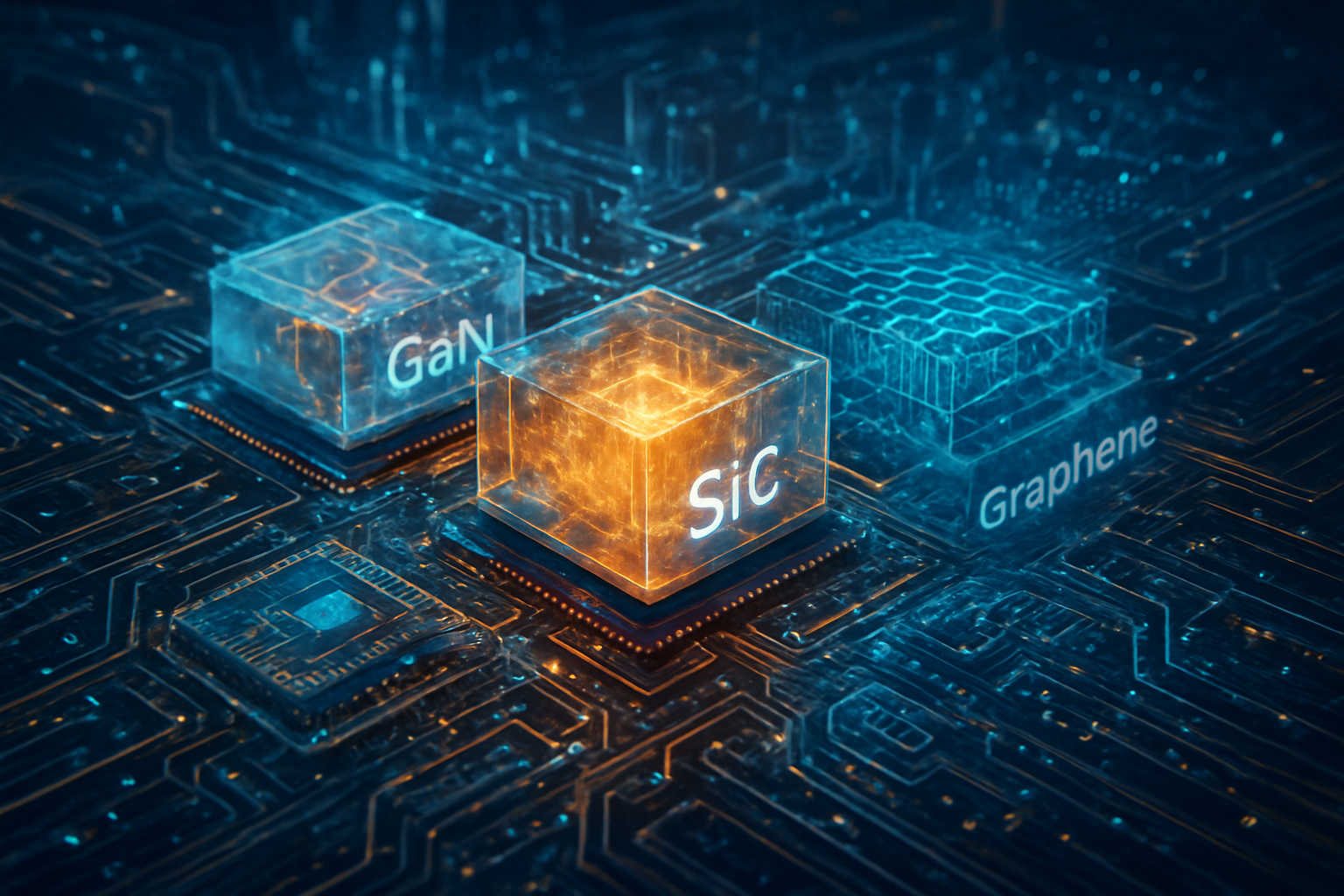
    The foundational material of the modern digital age, silicon, is rapidly approaching its inherent physical and performance limitations, heralding a pivotal shift in semiconductor fabrication. As the relentless demand for faster, smaller, and more energy-efficient chips intensifies, the tech industry is turning its gaze towards a promising new generation of materials. Gallium Nitride (GaN), Silicon Carbide (SiC), and two-dimensional (2D) materials like graphene are emerging as critical contenders to augment or even replace silicon, promising to unlock unprecedented advancements in computing power, energy efficiency, and miniaturization that are vital for the future of artificial intelligence, high-performance computing, and advanced electronics.

    This paradigm shift is not merely an incremental improvement but a fundamental re-evaluation of the building blocks of technology. The immediate significance of these emerging materials lies in their ability to shatter silicon's long-standing barriers, offering solutions to challenges that silicon simply cannot overcome. From powering the next generation of electric vehicles to enabling ultra-fast 5G/6G communication networks and creating more efficient data centers, these novel materials are poised to redefine what's possible in the world of semiconductors.

    The Technical Edge: Unpacking the Power of Next-Gen Materials

    Silicon's dominance for decades has been due to its abundance, excellent semiconductor properties, and well-established manufacturing processes. However, as transistors shrink to near-atomic scales, silicon faces insurmountable hurdles in miniaturization, power consumption, heat dissipation, and breakdown at high temperatures and voltages. This is where wide-bandgap (WBG) semiconductors like GaN and SiC, along with revolutionary 2D materials, step in, offering distinct advantages that silicon cannot match.

    Gallium Nitride (GaN), with a bandgap of 3.4 electron volts (eV) compared to silicon's 1.1 eV, is a game-changer for high-frequency and high-power applications. Its high electron mobility and saturation velocity allow GaN devices to switch up to 100 times faster than silicon, drastically reducing energy losses and boosting efficiency, particularly in power conversion systems. This translates to smaller, lighter, and more efficient power adapters (like those found in fast chargers), as well as significant energy savings in data centers and wireless infrastructure. GaN's superior thermal conductivity also means less heat generation and more effective dissipation, crucial for compact and reliable devices. The AI research community and industry experts have enthusiastically embraced GaN, recognizing its immediate impact on power electronics and its potential to enable more efficient AI hardware by reducing power overhead.

    Silicon Carbide (SiC), another WBG semiconductor with a bandgap of 3.3 eV, excels in extreme operating conditions. SiC devices can withstand significantly higher voltages (up to 10 times higher breakdown field strength than silicon) and temperatures, making them exceptionally robust for harsh environments. Its thermal conductivity is 3-4 times greater than silicon, which is vital for managing heavy loads in high-power applications such as electric vehicle (EV) inverters, solar inverters, and industrial motor drives. SiC semiconductors can reduce energy losses by up to 50% during power conversion, directly contributing to increased range and faster charging times for EVs. The automotive industry, in particular, has been a major driver for SiC adoption, with leading manufacturers integrating SiC into their next-generation electric powertrains, marking a clear departure from silicon-based power modules.

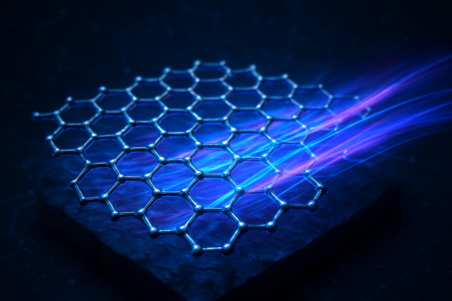
    Beyond WBG materials, two-dimensional (2D) materials like graphene and molybdenum disulfide (MoS2) represent the ultimate frontier in miniaturization. Graphene, a single layer of carbon atoms, boasts extraordinary electron mobility—up to 100 times that of silicon—and exceptional thermal conductivity, making it ideal for ultra-fast transistors and interconnects. While early graphene lacked an intrinsic bandgap, recent breakthroughs in engineering semiconducting graphene and the discovery of other 2D materials like MoS2 (with a stable bandgap nearly twice that of silicon) have reignited excitement. These atomically thin materials are paramount for pushing Moore's Law further, enabling novel 3D device architectures that can be stacked without significant performance degradation. The ability to create flexible and transparent electronics also opens doors for new form factors in wearable technology and advanced displays, garnering significant attention from leading research institutions and semiconductor giants for their potential to overcome silicon's ultimate scaling limits.

    Corporate Race: The Strategic Imperative for Tech Giants and Startups

    The shift towards non-silicon materials is igniting a fierce competitive race among semiconductor companies, tech giants, and innovative startups. Companies heavily invested in power electronics, automotive, and telecommunications stand to benefit immensely. Infineon Technologies AG (XTRA: IFX), STMicroelectronics N.V. (NYSE: STM), and ON Semiconductor Corporation (NASDAQ: ON) are leading the charge in SiC and GaN manufacturing, aggressively expanding production capabilities and R&D to meet surging demand from the electric vehicle and industrial sectors. These companies are strategically positioning themselves to dominate the high-growth markets for power management and conversion, where SiC and GaN offer unparalleled performance.

    For major AI labs and tech companies like NVIDIA Corporation (NASDAQ: NVDA), Intel Corporation (NASDAQ: INTC), and Taiwan Semiconductor Manufacturing Company Limited (NYSE: TSM), the implications are profound. While their primary focus remains on silicon for general-purpose computing, the adoption of GaN and SiC in power delivery and high-frequency components will enable more efficient and powerful AI accelerators and data center infrastructure. Intel, for instance, has been actively researching 2D materials for future transistor designs, aiming to extend the capabilities of its processors beyond silicon's physical limits. The ability to integrate these novel materials could lead to breakthroughs in energy efficiency for AI training and inference, significantly reducing operational costs and environmental impact. Startups specializing in GaN and SiC device fabrication, such as Navitas Semiconductor Corporation (NASDAQ: NVTS) and Wolfspeed, Inc. (NYSE: WOLF), are experiencing rapid growth, disrupting traditional silicon-centric supply chains with their specialized expertise and advanced manufacturing processes.

    The potential disruption to existing products and services is substantial. As GaN and SiC become more cost-effective and widespread, they will displace silicon in a growing number of applications where performance and efficiency are paramount. This could lead to a re-calibration of market share in power electronics, with companies that quickly adapt to these new material platforms gaining a significant strategic advantage. For 2D materials, the long-term competitive implications are even greater, potentially enabling entirely new categories of devices and computing paradigms that are currently impossible with silicon, pushing the boundaries of miniaturization and functionality. Companies that invest early and heavily in the research and development of these advanced materials are setting themselves up to define the next generation of technological innovation.

    A Broader Horizon: Reshaping the AI Landscape and Beyond

    The exploration of materials beyond silicon marks a critical juncture in the broader technological landscape, akin to previous monumental shifts in computing. This transition is not merely about faster chips; it underpins the continued advancement of artificial intelligence, edge computing, and sustainable energy solutions. The limitations of silicon have become a bottleneck for AI's insatiable demand for computational power and energy efficiency. Novel materials directly address this by enabling processors that run cooler, consume less power, and operate at higher frequencies, accelerating the development of more complex neural networks and real-time AI applications.

    The impacts extend far beyond the tech industry. In terms of sustainability, the superior energy efficiency of GaN and SiC devices can significantly reduce the carbon footprint of data centers, electric vehicles, and power grids. For instance, the widespread adoption of GaN in data center power supplies could lead to substantial reductions in global energy consumption and CO2 emissions, addressing pressing environmental concerns. The ability of 2D materials to enable extreme miniaturization and flexible electronics could also lead to advancements in medical implants, ubiquitous sensing, and personalized health monitoring, integrating technology more seamlessly into daily life.

    Potential concerns revolve around the scalability of manufacturing these new materials, their cost-effectiveness compared to silicon (at least initially), and the establishment of robust supply chains. While significant progress has been made, bringing these technologies to mass production with the same consistency and cost as silicon remains a challenge. However, the current momentum and investment indicate a strong commitment to overcoming these hurdles. This shift can be compared to the transition from vacuum tubes to transistors or from discrete components to integrated circuits—each marked a fundamental change that propelled technology forward by orders of magnitude. The move beyond silicon is poised to be another such transformative milestone, enabling the next wave of innovation across virtually every sector.

    The Road Ahead: Future Developments and Expert Predictions

    The trajectory for emerging semiconductor materials is one of rapid evolution and expanding applications. In the near term, we can expect to see continued widespread adoption of GaN and SiC in power electronics, particularly in electric vehicles, fast chargers, and renewable energy systems. The focus will be on improving manufacturing yields, reducing costs, and enhancing the reliability and performance of GaN and SiC devices. Experts predict a significant increase in the market share for these WBG semiconductors, with SiC dominating high-power, high-voltage applications and GaN excelling in high-frequency, medium-power domains.

    Longer term, the potential of 2D materials is immense. Research into graphene and other transition metal dichalcogenides (TMDs) will continue to push the boundaries of transistor design, aiming for atomic-scale devices that can operate at unprecedented speeds with minimal power consumption. The integration of 2D materials into existing silicon fabrication processes, potentially through monolithic 3D integration, is a key area of focus. This could lead to hybrid chips that leverage the best properties of both silicon and 2D materials, enabling novel architectures for quantum computing, neuromorphic computing, and ultra-dense memory. Challenges that need to be addressed include scalable and defect-free growth of large-area 2D materials, effective doping strategies, and reliable contact formation at the atomic scale.

    Experts predict that the next decade will witness a diversification of semiconductor materials, moving away from a silicon-monopoly towards a more specialized approach where different materials are chosen for their optimal properties in specific applications. We can anticipate breakthroughs in new material combinations, advanced packaging techniques for heterogeneous integration, and the development of entirely new device architectures. The ultimate goal is to enable a future where computing is ubiquitous, intelligent, and sustainable, with novel materials playing a crucial role in realizing this vision.

    A New Foundation for the Digital Age

    The journey beyond silicon represents a fundamental re-imagining of the building blocks of our digital world. The emergence of gallium nitride, silicon carbide, and 2D materials like graphene is not merely an incremental technological upgrade; it is a profound shift that promises to redefine the limits of performance, efficiency, and miniaturization in semiconductor devices. The key takeaway is clear: silicon's reign as the sole king of semiconductors is drawing to a close, making way for a multi-material future where specialized materials unlock unprecedented capabilities across diverse applications.

    This development is of immense significance in AI history, as it directly addresses the physical constraints that could otherwise impede the continued progress of artificial intelligence. By enabling more powerful, efficient, and compact hardware, these novel materials will accelerate advancements in machine learning, deep learning, and edge AI, allowing for more sophisticated and pervasive intelligent systems. The long-term impact will be felt across every industry, from enabling smarter grids and more sustainable energy solutions to revolutionizing transportation, healthcare, and communication.

    In the coming weeks and months, watch for further announcements regarding manufacturing scale-up for GaN and SiC, particularly from major players in the automotive and power electronics sectors. Keep an eye on research breakthroughs in 2D materials, especially concerning their integration into commercial fabrication processes and the development of functional prototypes. The race to master these new materials is on, and the implications for the future of technology are nothing short of revolutionary.


    This content is intended for informational purposes only and represents analysis of current AI developments.

    TokenRing AI delivers enterprise-grade solutions for multi-agent AI workflow orchestration, AI-powered development tools, and seamless remote collaboration platforms.
    For more information, visit https://www.tokenring.ai/.

  • The Atomic Revolution: New Materials Propel AI Semiconductors Beyond Silicon’s Limits

    The Atomic Revolution: New Materials Propel AI Semiconductors Beyond Silicon’s Limits

    The relentless march of artificial intelligence, demanding ever-greater computational power and energy efficiency, is pushing the very limits of traditional silicon-based semiconductors. As AI models grow in complexity and data centers consume prodigious amounts of energy, a quiet but profound revolution is unfolding in materials science. Researchers and industry leaders are now looking beyond silicon to a new generation of exotic materials – from atomically thin 2D compounds to 'memory-remembering' ferroelectrics and zero-resistance superconductors – that promise to unlock unprecedented performance and sustainability for the next wave of AI chips. This fundamental shift is not just an incremental upgrade but a foundational re-imagining of how AI hardware is built, with immediate and far-reaching implications for the entire technology landscape.

    This paradigm shift is driven by the urgent need to overcome the physical and energetic bottlenecks inherent in current silicon technology. As transistors shrink to atomic scales, quantum effects become problematic, and heat dissipation becomes a major hurdle. The new materials, each with unique properties, offer pathways to denser, faster, and dramatically more power-efficient AI processors, essential for everything from sophisticated generative AI models to ubiquitous edge computing devices. The race is on to integrate these innovations, heralding an era where AI's potential is no longer constrained by the limitations of a single element.

    The Microscopic Engineers: Specific Innovations and Their Technical Prowess

    The core of this revolution lies in the unique properties of several advanced material classes. Two-dimensional (2D) materials, such as graphene and hexagonal boron nitride (hBN), are at the forefront. Graphene, a single layer of carbon atoms, boasts ultra-high carrier mobility and exceptional electrical conductivity, making it ideal for faster electronic devices. Its counterpart, hBN, acts as an excellent insulator and substrate, enhancing graphene's performance by minimizing scattering. Their atomic thinness allows for unprecedented miniaturization, enabling denser chip designs and reducing the physical size limits faced by silicon, while also being crucial for energy-efficient, atomically thin artificial neurons in neuromorphic computing.

    Ferroelectric materials are another game-changer, characterized by their ability to retain electrical polarization even after an electric field is removed, effectively "remembering" their state. This non-volatility, combined with low power consumption and high endurance, makes them perfect for addressing the notorious "memory bottleneck" in AI. By creating ferroelectric RAM (FeRAM) and high-performance electronic synapses, these materials are enabling neuromorphic chips that mimic the human brain's adaptive learning and computation with significantly reduced energy overhead. Materials like hafnium-based thin films even become more robust at nanometer scales, promising ultra-small, efficient AI components.

    Superconducting materials represent the pinnacle of energy efficiency, exhibiting zero electrical resistance below a critical temperature. This means electric currents can flow indefinitely without energy loss, leading to potentially 100 times more energy efficiency and 1000 times more computational density than state-of-the-art CMOS processors. While typically requiring cryogenic temperatures, recent breakthroughs like germanium exhibiting superconductivity at 3.5 Kelvin hint at more accessible applications. Superconductors are also fundamental to quantum computing, forming the basis of Josephson junctions and qubits, which are critical for future quantum AI systems that demand unparalleled speed and precision.

    Finally, novel dielectrics are crucial insulators that prevent signal interference and leakage within chips. Low-k dielectrics, with their low dielectric constants, are essential for reducing capacitive coupling (crosstalk) as wiring becomes denser, enabling higher-speed communication. Conversely, certain high-κ dielectrics offer high permittivity, allowing for low-voltage, high-performance thin-film transistors. These advancements are vital for increasing chip density, improving signal integrity, and facilitating advanced 2.5D and 3D semiconductor packaging, ensuring that the benefits of new conductive and memory materials can be fully realized within complex chip architectures.

    Reshaping the AI Industry: Corporate Battlegrounds and Strategic Advantages

    The emergence of these new materials is creating a fierce new battleground for supremacy among AI companies, tech giants, and ambitious startups. Major semiconductor manufacturers like Taiwan Semiconductor Manufacturing Company (TSMC) (TWSE: 2330), Intel Corporation (NASDAQ: INTC), and Samsung Electronics Co., Ltd. (KRX: 005930) are heavily investing in researching and integrating these advanced materials into their future technology roadmaps. Their ability to successfully scale production and leverage these innovations will solidify their market dominance in the AI hardware space, giving them a critical edge in delivering the next generation of powerful and efficient AI chips.

    This shift also brings potential disruption to traditional silicon-centric chip design and manufacturing. Startups specializing in novel material synthesis or innovative device integration are poised to become key players or lucrative acquisition targets. Companies like Paragraf, which focuses on graphene-based electronics, and SuperQ Technologies, developing high-temperature superconductors, exemplify this new wave. Simultaneously, tech giants such as International Business Machines Corporation (NYSE: IBM) and Alphabet Inc. (NASDAQ: GOOGL) (Google) are pouring resources into superconducting quantum computing and neuromorphic chips, leveraging these materials to push the boundaries of their AI capabilities and maintain competitive leadership.

    The companies that master the integration of these materials will gain significant strategic advantages in performance, power consumption, and miniaturization. This is crucial for developing the increasingly sophisticated AI models that demand immense computational resources, as well as for enabling efficient AI at the edge in devices like autonomous vehicles and smart sensors. Overcoming the "memory bottleneck" with ferroelectrics or achieving near-zero energy loss with superconductors offers unparalleled efficiency gains, translating directly into lower operational costs for AI data centers and enhanced computational power for complex AI workloads.

    Research institutions like Imec in Belgium and Fraunhofer IPMS in Germany are playing a pivotal role in bridging the gap between fundamental materials science and industrial application. These centers, often in partnership with leading tech companies, are accelerating the development and validation of new material-based components. Furthermore, funding initiatives from bodies like the Defense Advanced Research Projects Agency (DARPA) underscore the national strategic importance of these material advancements, intensifying the global competitive race to harness their full potential for AI.

    A New Foundation for AI's Future: Broader Implications and Milestones

    These material innovations are not merely technical improvements; they are foundational to the continued exponential growth and evolution of artificial intelligence. By enabling the development of larger, more complex neural networks and facilitating breakthroughs in generative AI, autonomous systems, and advanced scientific discovery, they are crucial for sustaining the spirit of Moore's Law in an era where silicon is rapidly approaching its physical limits. This technological leap will underpin the next wave of AI capabilities, making previously unimaginable computational feats possible.

    The primary impacts of this revolution include vastly improved energy efficiency, a critical factor in mitigating the environmental footprint of increasingly powerful AI data centers. As AI scales, its energy demands become a significant concern; these materials offer a path toward more sustainable computing. Furthermore, by reducing the cost per computation, they could democratize access to higher AI capabilities. However, potential concerns include the complexity and cost of manufacturing these novel materials at industrial scale, the need for entirely new fabrication techniques, and potential supply chain vulnerabilities if specific rare materials become essential components.

    This shift in materials science can be likened to previous epoch-making transitions in computing history, such as the move from vacuum tubes to transistors, or the advent of integrated circuits. It represents a fundamental technological leap that will enable future AI milestones, much like how improvements in Graphics Processing Units (GPUs) fueled the deep learning revolution. The ability to create brain-inspired neuromorphic chips with ferroelectrics and 2D materials directly addresses the architectural limitations of traditional Von Neumann machines, paving the way for truly intelligent, adaptive systems that more closely mimic biological brains.

    The integration of AI itself into the discovery process for new materials further underscores the profound interconnectedness of these advancements. Institutions like the Johns Hopkins Applied Physics Laboratory (APL) and the National Institute of Standards and Technology (NIST) are leveraging AI to rapidly identify and optimize novel semiconductor materials, creating a virtuous cycle where AI helps build the very hardware that will power its future iterations. This self-accelerating innovation loop promises to compress development cycles and unlock material properties that might otherwise remain undiscovered.

    The Horizon of Innovation: Future Developments and Expert Outlook

    In the near term, the AI semiconductor landscape will likely feature hybrid chips that strategically incorporate novel materials for specialized functions. We can expect to see ferroelectric memory integrated alongside traditional silicon logic, or 2D material layers enhancing specific components within a silicon-based architecture. This allows for a gradual transition, leveraging the strengths of both established and emerging technologies. Long-term, however, the vision includes fully integrated chips built entirely from 2D materials or advanced superconducting circuits, particularly for groundbreaking applications in quantum computing and ultra-low-power edge AI devices. The continued miniaturization and efficiency gains will enable AI to be embedded in an even wider array of ubiquitous forms, from smart dust to advanced medical implants.

    The potential applications stemming from these material innovations are vast and transformative. They range from real-time, on-device AI processing for truly autonomous vehicles and smart city infrastructure, to massive-scale scientific simulations that can model complex biological systems or climate change scenarios with unprecedented accuracy. Personalized healthcare, advanced robotics, and immersive virtual realities will all benefit from the enhanced computational power and energy efficiency. However, significant challenges remain, including scaling up the manufacturing processes for these intricate new materials, ensuring their long-term reliability and yield in mass production, and developing entirely new chip architectures and software stacks that can fully leverage their unique properties. Interoperability with existing infrastructure and design tools will also be a key hurdle to overcome.

    Experts predict a future for AI semiconductors that is inherently multi-material, moving away from a single dominant material like silicon. The focus will be on optimizing specific material combinations and architectures for particular AI workloads, creating a highly specialized and efficient hardware ecosystem. The ongoing race to achieve stable room-temperature superconductivity or seamless, highly reliable 2D material integration continues, promising even more radical shifts in computing paradigms. Critically, the convergence of materials science, advanced AI, and quantum computing will be a defining trend, with AI acting as a catalyst for discovering and refining the very materials that will power its future, creating a self-reinforcing cycle of innovation.

    A New Era for AI: A Comprehensive Wrap-Up

    The journey beyond silicon to novel materials like 2D compounds, ferroelectrics, superconductors, and advanced dielectrics marks a pivotal moment in the history of artificial intelligence. This is not merely an incremental technological advancement but a foundational shift in how AI hardware is conceived, designed, and manufactured. It promises unprecedented gains in speed, energy efficiency, and miniaturization, which are absolutely critical for powering the next wave of AI innovation and addressing the escalating demands of increasingly complex models and data-intensive applications. This material revolution stands as a testament to human ingenuity, akin to earlier paradigm shifts that redefined the very nature of computing.

    The long-term impact of these developments will be a world where AI is more pervasive, powerful, and sustainable. By overcoming the current physical and energy bottlenecks, these material innovations will unlock capabilities previously confined to the realm of science fiction. From advanced robotics and immersive virtual realities to personalized medicine, climate modeling, and sophisticated generative AI, these new materials will underpin the essential infrastructure for truly transformative AI applications across every sector of society. The ability to process more information with less energy will accelerate scientific discovery, enable smarter infrastructure, and fundamentally alter how humans interact with technology.

    In the coming weeks and months, the tech world should closely watch for announcements from major semiconductor companies and leading research consortia regarding new material integration milestones. Particular attention should be paid to breakthroughs in 3D stacking technologies for heterogeneous integration and the unveiling of early neuromorphic chip prototypes that leverage ferroelectric or 2D materials. Keep an eye on advancements in manufacturing scalability for these novel materials, as well as the development of new software frameworks and programming models optimized for these emerging hardware architectures. The synergistic convergence of materials science, artificial intelligence, and quantum computing will undoubtedly be one of the most defining and exciting trends to follow in the unfolding narrative of technological progress.


    This content is intended for informational purposes only and represents analysis of current AI developments.

    TokenRing AI delivers enterprise-grade solutions for multi-agent AI workflow orchestration, AI-powered development tools, and seamless remote collaboration platforms.
    For more information, visit https://www.tokenring.ai/.

  • The Materials Race: Next-Gen Semiconductors Reshape AI, HPC, and Global Manufacturing

    The Materials Race: Next-Gen Semiconductors Reshape AI, HPC, and Global Manufacturing

    As the digital world hurries towards an era dominated by artificial intelligence, high-performance computing (HPC), and pervasive connectivity, the foundational material of modern electronics—silicon—is rapidly approaching its physical limits. A quiet but profound revolution is underway in material science and semiconductor manufacturing, with recent innovations in novel materials and advanced fabrication techniques promising to unlock unprecedented levels of chip performance, energy efficiency, and manufacturing agility. This shift, particularly prominent from late 2024 through 2025, is not merely an incremental upgrade but a fundamental re-imagining of how microchips are built, with far-reaching implications for every sector of technology.

    The immediate significance of these advancements cannot be overstated. From powering more intelligent AI models and enabling faster 5G/6G communication to extending the range of electric vehicles and enhancing industrial automation, these next-generation semiconductors are the bedrock upon which future technological breakthroughs will be built. The industry is witnessing a concerted global effort to invest in research, development, and new manufacturing plants, signaling a collective understanding that the future of computing lies "beyond silicon."

    The Science of Speed and Efficiency: A Deep Dive into Next-Gen Materials

    The core of this revolution lies in the adoption of materials with superior intrinsic properties compared to silicon. Wide-bandgap semiconductors, two-dimensional (2D) materials, and a host of other exotic compounds are now moving from laboratories to production lines, fundamentally altering chip design and capabilities.

    Wide-Bandgap Semiconductors: GaN and SiC Lead the Charge
    Gallium Nitride (GaN) and Silicon Carbide (SiC) are at the forefront of this material paradigm shift, particularly for high-power, high-frequency, and high-voltage applications. GaN, with its superior electron mobility, enables significantly faster switching speeds and higher power density. This makes GaN ideal for RF communication, 5G infrastructure, high-speed processors, and compact, efficient power solutions like fast chargers and electric vehicle (EV) components. GaN chips can operate up to 10 times faster than traditional silicon and contribute to a 10 times smaller CO2 footprint in manufacturing. In data center applications, GaN-based chips achieve 97-99% energy efficiency, a substantial leap from the approximately 90% for traditional silicon. Companies like Infineon Technologies AG (ETR: IFX), Taiwan Semiconductor Manufacturing Company (TSMC) (NYSE: TSM), and Navitas Semiconductor Corporation (NASDAQ: NVTS) are aggressively scaling up GaN production.

    SiC, on the other hand, is transforming power semiconductor design for high-voltage applications. It can operate at higher voltages and temperatures (above 200°C and over 1.2 kV) than silicon, with lower switching losses. This makes SiC indispensable for EVs, industrial automation, and renewable energy systems, leading to higher efficiency, reduced heat waste, and extended battery life. Wolfspeed, Inc. (NYSE: WOLF), a leader in SiC technology, is actively expanding its global production capacity to meet burgeoning demand.

    Two-Dimensional Materials: Graphene and TMDs for Miniaturization
    For pushing the boundaries of miniaturization and introducing novel functionalities, two-dimensional (2D) materials are gaining traction. Graphene, a single layer of carbon atoms, boasts exceptional electrical and thermal conductivity. Electrons move more quickly in graphene than in silicon, making it an excellent conductor for high-speed applications. A significant breakthrough in 2024 involved researchers successfully growing epitaxial semiconductor graphene monolayers on silicon carbide wafers, opening the energy bandgap of graphene—a long-standing challenge for its use as a semiconductor. Graphene photonics, for instance, can enable 1,000 times faster data transmission. Transition Metal Dichalcogenides (TMDs), such as Molybdenum Disulfide (MoS₂), naturally possess a bandgap, making them directly suitable for ultra-thin transistors, sensors, and flexible electronics, offering excellent energy efficiency in low-power devices.

    Emerging Materials and Manufacturing Innovations
    Beyond these, materials like Carbon Nanotubes (CNTs) promise smaller, faster, and more energy-efficient transistors. Researchers at MIT have identified cubic boron arsenide as a material that may outperform silicon in both heat and electricity conduction, potentially addressing two major limitations, though its commercial viability is still nascent. New indium-based materials are being developed for extreme ultraviolet (EUV) patterning in lithography, enabling smaller, more precise features and potentially 3D circuits. Even the accidental discovery of a superatomic material (Re₆Se₈Cl₂) by Columbia University researchers, which exhibits electron movement potentially up to a million times faster than in silicon, hints at the vast untapped potential in material science.

    Crucially, glass substrates are revolutionizing chip packaging by allowing for higher interconnect density and the integration of more chiplets into a single package, facilitating larger, more complex assemblies for data-intensive applications. Manufacturing processes themselves are evolving with advanced lithography (EUV with new photoresists), advanced packaging (chiplets, 2.5D, and 3D stacking), and the increasing integration of AI and machine learning for automation, optimization, and defect detection, accelerating the design and production of complex chips.

    Competitive Implications and Market Shifts in the AI Era

    These material science breakthroughs and manufacturing innovations are creating significant competitive advantages and reshaping the landscape for AI companies, tech giants, and startups alike.

    Companies deeply invested in high-power and high-frequency applications, such as those in the automotive (EVs), renewable energy, and 5G/6G infrastructure sectors, stand to benefit immensely from GaN and SiC. Automakers adopting SiC in their power electronics will see improved EV range and charging times, while telecommunications companies deploying GaN can build more efficient and powerful base stations. Power semiconductor manufacturers like Wolfspeed and Infineon, with their established expertise and expanding production, are poised to capture significant market share in these growing segments.

    For AI and HPC, the push for faster, more energy-efficient processors makes materials like graphene, TMDs, and advanced packaging solutions critical. Tech giants like NVIDIA Corporation (NASDAQ: NVDA), Intel Corporation (NASDAQ: INTC), and Advanced Micro Devices, Inc. (NASDAQ: AMD), who are at the forefront of AI accelerator development, will leverage these innovations to deliver more powerful and sustainable computing platforms. The ability to integrate diverse chiplets (CPUs, GPUs, AI accelerators) using advanced packaging techniques, spearheaded by TSMC (NYSE: TSM) with its CoWoS (Chip-on-Wafer-on-Substrate) technology, allows for custom, high-performance solutions tailored for specific AI workloads. This heterogeneous integration reduces reliance on monolithic chip designs, offering flexibility and performance gains previously unattainable.

    Startups focused on novel material synthesis, advanced packaging design, or specialized AI-driven manufacturing tools are also finding fertile ground. These smaller players can innovate rapidly, potentially offering niche solutions that complement the larger industry players or even disrupt established supply chains. The "materials race" is now seen as the new Moore's Law, shifting the focus from purely lithographic scaling to breakthroughs in materials science, which could elevate companies with strong R&D in this area. Furthermore, the emphasis on energy efficiency driven by these new materials directly addresses the growing power consumption concerns of large-scale AI models and data centers, offering a strategic advantage to companies that can deliver sustainable computing solutions.

    A Broader Perspective: Impact and Future Trajectories

    These semiconductor material innovations fit seamlessly into the broader AI landscape, acting as a crucial enabler for the next generation of intelligent systems. The insatiable demand for computational power to train and run ever-larger AI models, coupled with the need for efficient edge AI devices, makes these material advancements not just desirable but essential. They are the physical foundation for achieving greater AI capabilities, from real-time data processing in autonomous vehicles to more sophisticated natural language understanding and generative AI.

    The impacts are profound: faster inference speeds, reduced latency, and significantly lower energy consumption for AI workloads. This translates to more responsive AI applications, lower operational costs for data centers, and the proliferation of AI into power-constrained environments like wearables and IoT devices. Potential concerns, however, include the complexity and cost of manufacturing these new materials, the scalability of some emerging compounds, and the environmental footprint of new chemical processes. Supply chain resilience also remains a critical geopolitical consideration, especially with the global push for localized fab development.

    These advancements draw comparisons to previous AI milestones where hardware breakthroughs significantly accelerated progress. Just as specialized GPUs revolutionized deep learning, these new materials are poised to provide the next quantum leap in processing power and efficiency, moving beyond the traditional silicon-centric bottlenecks. They are not merely incremental improvements but fundamental shifts that redefine what's possible in chip design and, consequently, in AI.

    The Horizon: Anticipated Developments and Expert Predictions

    Looking ahead, the trajectory of semiconductor material innovation is set for rapid acceleration. In the near-term, expect to see wider adoption of GaN and SiC across various industries, with increased production capacities coming online through late 2025 and into 2026. TSMC (NYSE: TSM), for instance, plans to begin volume production of its 2nm process in late 2025, heavily relying on advanced materials and lithography. We will also witness a significant expansion in advanced packaging solutions, with chiplet architectures becoming standard for high-performance processors, further blurring the lines between different chip types and enabling unprecedented integration.

    Long-term developments will likely involve the commercialization of more exotic materials like graphene, TMDs, and potentially even cubic boron arsenide, as manufacturing challenges are overcome. The development of AI-designed materials for HPC is also an emerging market, promising improvements in thermal management, interconnect density, and mechanical reliability in advanced packaging solutions. Potential applications include truly flexible electronics, self-powering sensors, and quantum computing materials that can improve qubit coherence and error correction.

    Challenges that need to be addressed include the cost-effective scaling of these novel materials, the development of robust and reliable manufacturing processes, and the establishment of resilient supply chains. Experts predict a continued "materials race," where breakthroughs in material science will be as critical as advancements in lithography for future progress. The convergence of material science, advanced packaging, and AI-driven design will define the next decade of semiconductor innovation, enabling capabilities that are currently only theoretical.

    A New Era of Computing: The Unfolding Story

    In summary, the ongoing revolution in semiconductor materials represents a pivotal moment in the history of computing. The move beyond silicon to wide-bandgap semiconductors like GaN and SiC, coupled with the exploration of 2D materials and other exotic compounds, is fundamentally enhancing chip performance, energy efficiency, and manufacturing flexibility. These advancements are not just technical feats; they are the essential enablers for the next wave of artificial intelligence, high-performance computing, and ubiquitous connectivity, promising a future where computing power is faster, more efficient, and seamlessly integrated into every aspect of life.

    The significance of this development in AI history cannot be overstated; it provides the physical muscle for the intelligent algorithms that are transforming our world. As global investments pour into new fabs, particularly in the U.S., Japan, Europe, and India, and material science R&D intensifies, the coming months and years will reveal the full extent of this transformation. Watch for continued announcements regarding new material commercialization, further advancements in advanced packaging technologies, and the increasing integration of AI into the very process of chip design and manufacturing. The materials race is on, and its outcome will shape the digital future.


    This content is intended for informational purposes only and represents analysis of current AI developments.

    TokenRing AI delivers enterprise-grade solutions for multi-agent AI workflow orchestration, AI-powered development tools, and seamless remote collaboration platforms.
    For more information, visit https://www.tokenring.ai/.