Tag: Green Energy

  • The End of the Silicon Age: How GaN and SiC are Electrifying the 2026 Green Energy Revolution

    The End of the Silicon Age: How GaN and SiC are Electrifying the 2026 Green Energy Revolution

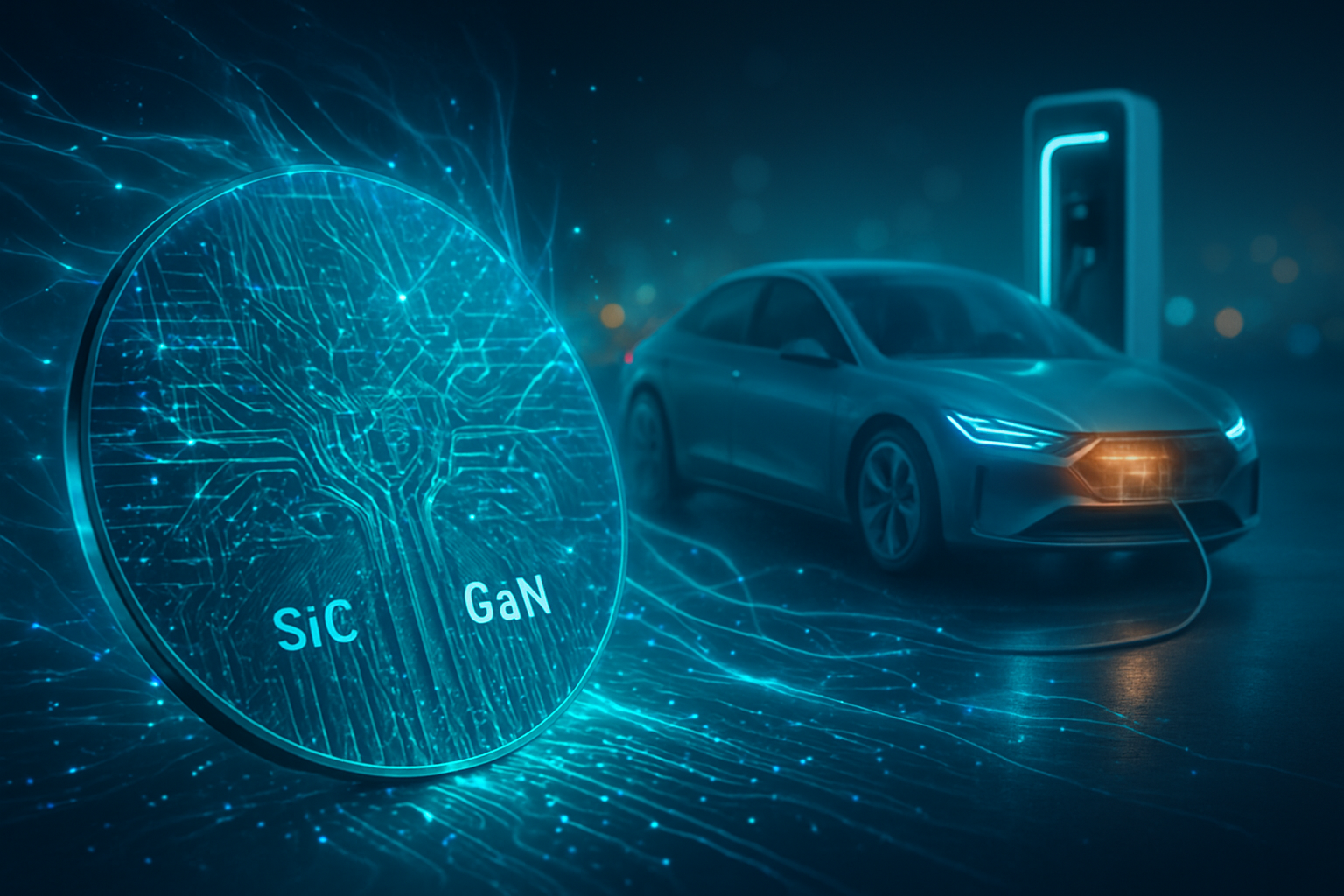
    The global transition to sustainable energy has reached a pivotal tipping point this week as the foundational hardware of the electric vehicle (EV) industry undergoes its most significant transformation in decades. On January 14, 2026, Mitsubishi Electric (OTC: MIELY) announced it would begin shipping samples of its newest trench Silicon Carbide (SiC) MOSFET bare dies on January 21, marking a definitive shift away from traditional silicon-based power electronics. This development is not merely a marginal improvement; it represents a fundamental re-engineering of how energy is managed, moving the industry toward "wide-bandgap" (WBG) materials that promise to unlock unprecedented range for EVs and near-instantaneous charging speeds.

    As of early 2026, the era of "Good Enough" silicon is officially over for high-performance applications. The rapid deployment of Gallium Nitride (GaN) and Silicon Carbide (SiC) in everything from 800V vehicle architectures to 500kW ultra-fast chargers is slashing energy waste and enabling a leaner, more efficient "green" grid. With Mitsubishi’s latest shipment of 750V and 1200V trench-gate dies, the industry is witnessing a "50-70-90" shift: a 50% reduction in power loss compared to previous-gen SiC, a 70% reduction compared to traditional silicon, and a push toward 99% total system efficiency in power conversion.

    The Trench Revolution: Technical Leaps in Power Density

    The technical core of this transition lies in the move from "Planar" to "Trench" architectures in SiC MOSFETs. Mitsubishi Electric's new bare dies, including the 750V WF0020P-0750AA series, utilize a proprietary trench structure where gate electrodes are etched vertically into the wafer. This design drastically increases cell density and reduces "on-resistance," the primary culprit behind heat generation and energy loss. Unlike traditional Silicon Insulated-Gate Bipolar Transistors (Si-IGBTs), which have dominated the industry for 30 years, these SiC devices can handle significantly higher voltages and temperatures while maintaining a footprint that is nearly 60% smaller.

    Beyond SiC, Gallium Nitride (GaN) has made its own breakthrough into the 800V EV domain. Historically relegated to consumer electronics and low-power chargers, new "Vertical GaN" architectures launched in late 2025 now allow GaN to operate at 1200V+ levels. While SiC remains the "muscle" for the main traction inverters that drive a car's wheels, GaN has become the "speedster" for onboard chargers (OBC) and DC-DC converters. Because GaN can switch at frequencies in the megahertz range—orders of magnitude faster than silicon—it allows for much smaller passive components, such as transformers and inductors. This "miniaturization" has led to a 40% reduction in the weight of power electronics in 2026 model-year vehicles, directly translating to more miles per kilowatt-hour.

    Initial reactions from the power electronics community have been overwhelmingly positive. Dr. Elena Vance, a senior semiconductor analyst, noted that "the efficiency gains we are seeing with the 2026 trench-gate chips are the equivalent of adding 30-40 miles of range to an EV without increasing the battery size." Furthermore, the use of "Oblique Ion Implantation" in Mitsubishi's process has solved the long-standing trade-off between power loss and short-circuit robustness, a technical hurdle that had previously slowed the adoption of SiC in the most demanding automotive environments.

    A New Hierarchy: Market Leaders and the 300mm Race

    The shift to WBG materials has completely redrawn the competitive map of the semiconductor industry. STMicroelectronics (NYSE: STM) has solidified its lead as the dominant SiC supplier, capturing nearly 45% of the automotive market through its massive vertically integrated production hub in Catania, Italy. However, the most disruptive market move of 2026 came from Infineon Technologies (OTC: IFNNY), which recently operationalized the world’s first 300mm (12-inch) power GaN production line. This allows for a 2.3x higher chip yield per wafer, effectively commoditizing high-efficiency power chips that were once considered luxury components.

    The landscape also features a reborn Wolfspeed (NYSE: WOLF), which emerged from a 2025 restructuring as a "pure-play" SiC powerhouse. Operating the world’s largest fully automated 200mm fab in New York, Wolfspeed is now focusing on the high-end 1200V+ market required for heavy-duty trucking and AI data centers. Meanwhile, specialized players like Navitas Semiconductor (NASDAQ: NVTS) are dominating the "GaNFast" integrated circuit market, pushing the efficiency of 500kW fast chargers to the "Golden 99%" mark. This level of efficiency is critical because it eliminates the need for massive, expensive liquid cooling systems in chargers, allowing for slimmer, more reliable "plug-and-go" infrastructure.

    Strategic partnerships are also shifting. Automakers like Tesla (NASDAQ: TSLA) and BYD (OTC: BYDDF) are increasingly moving away from buying discrete components and are instead co-developing custom "power modules" with companies like onsemi (NASDAQ: ON). This vertical integration allows OEMs to optimize the thermal management of the SiC/GaN chips specifically for their unique chassis designs, further widening the gap between legacy manufacturers and the new "software-and-silicon" defined car companies.

    AI and the Grid: The Brains Behind the Power

    The "Green Energy Transition" is no longer just about better materials; it is increasingly about the intelligence controlling them. In 2026, the integration of Edge AI into power modules has become the standard. Mitsubishi's 1700V modules now feature Real-Time Control (RTC) circuits that use machine learning algorithms to predict and prevent short-circuits within nanoseconds. This "Smart Power" approach allows the system to push the SiC chips to their physical limits while maintaining a safety buffer that was previously impossible.

    This development fits into a broader trend where AI optimizes the entire energy lifecycle. In the 500kW fast chargers appearing at highway hubs this year, AI-driven switching optimization dynamically adjusts the frequency of the GaN/SiC switches based on the vehicle's state-of-charge and the grid's current load. This reduces "switching stress" and extends the lifespan of the charger by up to 30%. Furthermore, Deep Learning is now used in the manufacturing of these chips themselves; companies like Applied Materials use AI to scan SiC crystals for microscopic "killer defects," bringing the yield of high-voltage wafers closer to that of traditional silicon and lowering the cost for the end consumer.

    The wider significance of this shift cannot be overstated. By reducing the heat loss in power conversion, the world is effectively "saving" terawatts of energy that would have otherwise been wasted as heat. In an era where AI data centers are putting unprecedented strain on the electrical grid, the efficiency gains provided by SiC and GaN are becoming a critical pillar of global energy security, ensuring that the transition to EVs does not collapse the existing power infrastructure.

    Looking Ahead: The Road to 1.2MW and Beyond

    As we move deeper into 2026, the next frontier for WBG materials is the Megawatt Charging System (MCS) for commercial shipping and aviation. Experts predict that the 1700V and 3300V SiC MOSFETs currently being sampled by Mitsubishi and its peers will be the backbone of 1.2MW charging stations, capable of refilling a long-haul electric semi-truck in under 20 minutes. These high-voltage systems will require even more advanced "SBD-embedded" MOSFETs, which integrate Schottky Barrier Diodes directly into the chip to maximize power density.

    On the horizon, the industry is already looking toward "Gallium Oxide" (Ga2O3) as a potential successor to SiC in the 2030s, offering even wider bandgaps for ultra-high-voltage applications. However, for the next five years, the focus will remain on the maturation of the GaN-on-Silicon and SiC-on-SiC ecosystems. The primary challenge remains the supply chain of raw materials, particularly the high-purity carbon and silicon required for SiC crystal growth, leading many nations to designate these semiconductors as "critical strategic assets."

    A New Standard for a Greener Future

    The shipment of Mitsubishi Electric’s latest SiC samples this week is more than a corporate milestone; it is a signpost for the end of the Silicon Age in power electronics. The transition to GaN and SiC has enabled a 70% reduction in power losses, a 5-7% increase in EV range, and the birth of 500kW fast-charging networks that finally rival the convenience of gasoline.

    As we look toward the remainder of 2026, the key developments to watch will be the scaling of 300mm GaN production and the integration of these high-efficiency chips into the "smart grid." The significance of this breakthrough in technology history will likely be compared to the transition from vacuum tubes to transistors—a fundamental shift that makes the "impossible" (like a 600-mile range EV that charges in 10 minutes) a standard reality. The green energy transition is now being fueled by the smallest of switches, and they are faster, cooler, and more efficient than ever before.


    This content is intended for informational purposes only and represents analysis of current technology and market developments.

    TokenRing AI delivers enterprise-grade solutions for multi-agent AI workflow orchestration, AI-powered development tools, and seamless remote collaboration platforms.
    For more information, visit https://www.tokenring.ai/.

  • AI-Driven “Computational Alchemy”: How Meta and Google are Reimagining the Periodic Table

    AI-Driven “Computational Alchemy”: How Meta and Google are Reimagining the Periodic Table

    The centuries-old process of material discovery—a painstaking cycle of trial, error, and serendipity—has been fundamentally disrupted. In a series of breakthroughs that experts are calling the dawn of "computational alchemy," tech giants are using artificial intelligence to predict millions of new stable crystals, effectively mapping out the next millennium of materials science in a matter of months. This shift from physical experimentation to AI-first simulation is not merely a laboratory curiosity; it is the cornerstone of a global race to develop the next generation of solid-state batteries, high-efficiency solar cells, and room-temperature superconductors.

    As of early 2026, the landscape of materials science has been rewritten by two primary forces: Google DeepMind’s GNoME and Meta’s OMat24. These models have expanded the library of known stable materials from roughly 48,000 to over 2.2 million. By bypassing the grueling requirements of traditional quantum mechanical calculations, these AI systems are identifying the "needles in the haystack" that could solve the climate crisis, providing the blueprints for hardware that can store more energy, harvest more sunlight, and transmit electricity with zero loss.

    The Technical Leap: From Message-Passing to Equivariant Transformers

    The technical foundation of this revolution lies in the transition from Density Functional Theory (DFT)—the "gold standard" of physics-based simulation—to AI surrogate models. Traditional DFT is computationally expensive, often taking days or weeks to simulate the stability of a single crystal structure. In contrast, Google DeepMind’s Alphabet Inc. (NASDAQ: GOOGL) GNoME (Graph Networks for Materials Exploration) utilizes Graph Neural Networks (GNNs) to predict the stability of materials in milliseconds. GNoME’s architecture employs a "symmetry-aware" structural pipeline and a compositional pipeline, which together have identified 381,000 "highly stable" crystals that lie on the thermodynamic convex hull.

    While Google focused on the sheer scale of discovery, Meta Platforms Inc. (NASDAQ: META) took a different approach with its OMat24 (Open Materials 2024) release. Utilizing the EquiformerV2 architecture—an equivariant transformer—Meta’s models are designed to be "E(3) equivariant." This means the AI’s internal representations remain consistent regardless of how a crystal is rotated or translated in 3D space, a critical requirement for physical accuracy. Furthermore, OMat24 provided the research community with a massive open-source dataset of 110 million DFT calculations, including "non-equilibrium" structures—atoms caught in the middle of vibrating or reacting. This data is essential for Molecular Dynamics (MD), allowing scientists to simulate how a material behaves at extreme temperatures or under the high pressures found inside a solid-state battery.

    The industry consensus has shifted rapidly. Where researchers once debated whether AI could match the accuracy of physics-first models, they are now focused on "Active Learning Flywheels." In these systems, AI predicts a material, a robotic lab (like the A-Lab at Lawrence Berkeley National Laboratory) attempts to synthesize it, and the results—success or failure—are fed back into the AI to refine its next prediction. This closed-loop system has already achieved a 71% success rate in synthesizing previously unknown materials, a feat that would have been impossible three years ago.

    The Corporate Race for "AI for Science" Dominance

    The strategic positioning of the "Big Three"—Alphabet, Meta, and Microsoft Corp. (NASDAQ: MSFT)—reveals a high-stakes battle for the future of industrial R&D. Alphabet, through DeepMind, has positioned itself as the "Scientific Instrument" provider. By integrating GNoME’s 381,000 stable materials into the public Materials Project, Google is setting the standard for the entire field. Its recent announcement of a Gemini-powered autonomous research lab in the UK, set to reach full operational capacity later in 2026, signals a move toward vertical integration: Google will not just predict the materials; it will own the robotic infrastructure that discovers them.

    Microsoft has adopted a more product-centric "Economic Platform" strategy. Through its MatterGen and MatterSim models, Microsoft is focusing on immediate industrial applications. Its partnership with the Pacific Northwest National Laboratory (PNNL) has already yielded a new solid-state battery material that reduces lithium usage by 70%. By framing AI as a tool to solve specific supply chain bottlenecks, Microsoft is courting the automotive and energy sectors, positioning its Azure Quantum platform as the indispensable operating system for the green energy transition.

    Meta, conversely, is doubling down on the "Open Ecosystem" model. By releasing OMat24 and the subsequent 2025 Universal Model for Atoms (UMA), Meta is providing the foundational data that startups and academic labs need to compete. This strategy serves a dual purpose: it accelerates global material innovation—which Meta needs to lower the cost of the massive hardware infrastructure required for its metaverse and AI ambitions—while positioning the company as a benevolent leader in open-source science. This "infrastructure of discovery" approach ensures that even if Meta doesn't discover the next room-temperature superconductor itself, the discovery will likely happen using Meta’s tools.

    Broader Significance: The "Genesis Mission" and the Green Transition

    The impact of these AI developments extends far beyond the balance sheets of tech companies. We are witnessing the birth of "AI4Science" as a dominant geopolitical and environmental trend. In late 2024 and throughout 2025, the U.S. Department of Energy launched the "Genesis Mission," often described as a "Manhattan Project for AI." This initiative, which includes partners like Alphabet, Microsoft, and Nvidia Corp. (NASDAQ: NVDA), aims to harness AI to solve 20 national science challenges by 2026, with a primary focus on grid-scale energy storage and carbon capture.

    This shift represents a fundamental change in the broader AI landscape. For years, the primary focus of Large Language Models (LLMs) was generating text and images. Now, the frontier has moved to "Physical AI"—models that understand the laws of physics and chemistry. This transition is essential for the green energy transition. Current lithium-ion batteries are reaching their theoretical limits, and silicon-based solar cells are plateauing in efficiency. AI-driven discovery is the only way to rapidly iterate through the quadrillions of possible chemical combinations to find the halide perovskites or solid electrolytes needed to reach Net Zero targets.

    However, this rapid progress is not without concerns. The "black box" nature of some AI predictions can make it difficult for scientists to understand why a material is stable, potentially leading to a "reproducibility crisis" in computational chemistry. Furthermore, as the most powerful models require immense compute resources, there is a growing "compute divide" between well-funded corporate labs and public universities, a gap that initiatives like Meta’s OMat24 are desperately trying to bridge.

    Future Horizons: From Lab-to-Fab and Gemini-Powered Robotics

    Looking toward the remainder of 2026 and beyond, the focus is shifting from "prediction" to "realization." The industry is moving into the "Lab-to-Fab" phase, where the challenge is no longer finding a stable crystal, but figuring out how to manufacture it at scale. We expect to see the first commercial prototypes of "AI-designed" solid-state batteries in high-end electric vehicles by late 2026. These batteries will likely feature the lithium-reduced electrolytes predicted by Microsoft’s MatterGen or the stable conductors identified by GNoME.

    On the horizon, the integration of multi-modal AI—like Google’s Gemini or OpenAI’s GPT-5—with laboratory robotics will create "Scientist Agents." These agents will not only predict materials but will also write the synthesis protocols, troubleshoot failed experiments in real-time using computer vision, and even draft the peer-reviewed papers. Experts predict that by 2027, the time required to bring a new material from initial discovery to a functional prototype will have dropped from the historical average of 20 years to less than 18 months.

    The next major milestone to watch is the discovery of a commercially viable, ambient-pressure superconductor. While the "LK-99" craze of 2023 was a false start, the systematic search being conducted by models like MatterGen and GNoME has already identified over 50 new chemical systems with superconducting potential. If even one of these proves successful and scalable, it would revolutionize everything from quantum computing to global power grids.

    A New Era of Accelerated Discovery

    The achievements of Meta’s OMat24 and Google’s GNoME represent a pivot point in human history. We have moved from being "gatherers" of materials—using what we find in nature or stumble upon in the lab—to being "architects" of matter. By mapping the vast "chemical space" of the universe, AI is providing the tools to build a sustainable future that was previously constrained by the slow pace of human experimentation.

    As we look ahead, the significance of these developments will likely be compared to the invention of the microscope or the telescope. AI is a new lens that allows us to see into the atomic structure of the world, revealing possibilities for energy and technology that were hidden in plain sight for centuries. In the coming months, the focus will remain on the "Genesis Mission" and the first results from the UK’s automated A-Labs. The race to reinvent the physical world is no longer a marathon; thanks to AI, it has become a sprint.


    This content is intended for informational purposes only and represents analysis of current AI developments.

    TokenRing AI delivers enterprise-grade solutions for multi-agent AI workflow orchestration, AI-powered development tools, and seamless remote collaboration platforms.
    For more information, visit https://www.tokenring.ai/.

  • The Silicon Green Rush: How Texas and Gujarat are Powering the AI Revolution with Clean Energy

    The Silicon Green Rush: How Texas and Gujarat are Powering the AI Revolution with Clean Energy

    As the global demand for artificial intelligence reaches a fever pitch, the semiconductor industry is facing an existential reckoning: how to produce the world’s most advanced chips without exhausting the planet’s resources. In a landmark shift for 2025, the industry’s two most critical growth hubs—Texas and Gujarat, India—have become the front lines for a new era of "Green Fabs." These multi-billion dollar manufacturing sites are no longer just about transistor density; they are being engineered as self-sustaining ecosystems powered by massive solar and wind arrays to mitigate the staggering environmental costs of AI hardware production.

    The immediate significance of this transition cannot be overstated. With the International Energy Agency (IEA) warning that data center electricity consumption could double to nearly 1,000 TWh by 2030, the "embodied carbon" of the chips themselves has become a primary concern for tech giants. By integrating renewable energy directly into the fabrication process, companies like Samsung Electronics (KRX: 005930), Texas Instruments (NASDAQ: TXN), and the Tata Group are attempting to decouple the explosive growth of AI from its carbon footprint, effectively rebranding silicon as a "low-carbon" commodity.

    Technical Foundations: The Rise of the Sustainable Mega-Fab

    The technical complexity of a modern semiconductor fab is unparalleled, requiring millions of gallons of ultrapure water (UPW) and gigawatts of electricity to operate. In Texas, Samsung’s Taylor facility—a $40 billion investment—is setting a new benchmark for resource efficiency. The site, which began installing equipment for 2nm chip production in late 2024, utilizes a "closed-loop" water system designed to reclaim and reuse up to 75% of process water. This is a critical advancement over legacy fabs, which often discharged millions of gallons of wastewater daily. Furthermore, Samsung has leveraged its participation in the RE100 initiative to secure 100% renewable electricity for its U.S. operations through massive Power Purchase Agreements (PPAs) with Texas wind and solar providers.

    Across the globe in Gujarat, India, Tata Electronics has broken ground on the country’s first "Mega Fab" in the Dholera Special Investment Region. This facility is uniquely positioned within one of the world’s largest renewable energy zones, drawing power from the Dholera Solar Park. In partnership with Powerchip Semiconductor Manufacturing Corp (PSMC), Tata is implementing "modularization" in its construction to reduce the carbon footprint of the build-out phase. The technical goal is to achieve near-zero liquid discharge (ZLD) from day one, a necessity in the water-scarce climate of Western India. These "greenfield" projects differ from older "brownfield" upgrades because sustainability is baked into the architectural DNA of the plant, utilizing AI-driven "digital twin" models to optimize energy flow in real-time.

    Initial reactions from the industry have been overwhelmingly positive, though tempered by the scale of the challenge. Analysts at TechInsights noted in late 2025 that the shift to High-NA EUV (Extreme Ultraviolet) lithography—while energy-intensive—is actually a "green" win. These machines, produced by ASML (NASDAQ: ASML), allow for single-exposure patterning that eliminates dozens of chemical-heavy processing steps, effectively reducing the energy used per wafer by an estimated 200 kWh.

    Strategic Positioning: Sustainability as a Competitive Moat

    The move toward green manufacturing is not merely an altruistic endeavor; it is a calculated strategic play. As major AI players like Nvidia (NASDAQ: NVDA), Apple (NASDAQ: AAPL), and Tesla (NASDAQ: TSLA) face tightening ESG (Environmental, Social, and Governance) reporting requirements, such as the EU’s Corporate Sustainability Reporting Directive (CSRD), they are increasingly favoring suppliers who can provide "low-carbon silicon." For these companies, the carbon footprint of their supply chain (Scope 3 emissions) is the hardest to control, making a green fab in Texas or Gujarat a highly attractive partner.

    Texas Instruments has already capitalized on this trend. As of December 17, 2025, TI announced that its 300mm manufacturing operations are now 100% powered by renewable energy. By providing clients with precise carbon-intensity data per chip, TI has created "transparency as a service," allowing Apple to calculate the exact footprint of the power management chips used in the latest iPhones. This level of data granularity has become a significant competitive advantage, potentially disrupting older fabs that cannot provide such detailed environmental metrics.

    In India, Tata Electronics is positioning itself as a "georesilient" and sustainable alternative to East Asian manufacturing hubs. By offering 100% green-powered production, Tata is courting Western firms looking to diversify their supply chains while maintaining their net-zero commitments. This market positioning is particularly relevant for the AI sector, where the "energy crisis" of training large language models (LLMs) has put a spotlight on the environmental ethics of the entire hardware stack.

    The Wider Significance: Mitigating the AI Energy Crisis

    The integration of clean energy into fab projects fits into a broader global trend of "Green AI." For years, the focus was solely on making AI models more efficient (algorithmic efficiency). However, the industry has realized that the hardware itself is the bottleneck. The environmental challenges are daunting: a single modern fab can consume as much water as a small city. In Gujarat, the government has had to commission a dedicated desalination plant for the Dholera region to ensure that the semiconductor industry doesn't compete with local agriculture for water.

    There are also potential concerns regarding "greenwashing" and the reliability of renewable grids. Solar and wind are intermittent, while a semiconductor fab requires 24/7 "five-nines" reliability—99.999% uptime. To address this, 2025 has seen a surge in interest in Small Modular Reactors (SMRs) and advanced battery storage to provide carbon-free baseload power. This marks a significant departure from previous industry milestones; while the 2010s were defined by the "mobile revolution" and a focus on battery life, the 2020s are being defined by the "AI revolution" and a focus on planetary sustainability.

    The ethical implications are also coming to the fore. As fabs move into regions like Texas and Gujarat, they bring high-paying jobs but also place immense pressure on local utilities. The "Texas Miracle" of low-cost energy is being tested by the sheer volume of new industrial demand, leading to a complex dialogue between tech giants, local communities, and environmental advocates regarding who gets priority during grid-stress events.

    Future Horizons: From Solar Parks to Nuclear Fabs

    Looking ahead to 2026 and beyond, the industry is expected to move toward even more radical energy solutions. Experts predict that the next generation of fabs will likely feature on-site nuclear micro-reactors to ensure a steady stream of carbon-free energy. Microsoft (NASDAQ: MSFT) and Intel (NASDAQ: INTC) have already begun exploring such partnerships, signaling that the "solar/wind" era may be just the first step in a longer journey toward energy independence for the semiconductor sector.

    Another frontier is the development of "circular silicon." Companies are researching ways to reclaim rare earth metals and high-purity chemicals from decommissioned chips and manufacturing waste. If successful, this would transition the industry from a linear "take-make-waste" model to a circular economy, further reducing the environmental impact of the AI revolution. The challenge remains the extreme purity required for chipmaking; any recycled material must meet the same "nine-nines" (99.9999999%) purity standards as virgin material.

    Conclusion: A New Standard for the AI Era

    The transition to clean-energy-powered fabs in Gujarat and Texas represents a watershed moment in the history of technology. It is a recognition that the "intelligence" provided by AI cannot come at the cost of the environment. The key takeaways from 2025 are clear: sustainability is now a core technical specification, water recycling is a prerequisite for expansion, and "low-carbon silicon" is the new gold standard for the global supply chain.

    As we look toward 2026, the industry’s success will be measured not just by Moore’s Law, but by its ability to scale responsibly. The "Green AI" movement has successfully moved from the fringe to the center of corporate strategy, and the massive projects in Texas and Gujarat are the physical manifestations of this shift. For investors, policymakers, and consumers, the message is clear: the future of AI is being written in silicon, but it is being powered by the sun and the wind.


    This content is intended for informational purposes only and represents analysis of current AI developments.

    TokenRing AI delivers enterprise-grade solutions for multi-agent AI workflow orchestration, AI-powered development tools, and seamless remote collaboration platforms.
    For more information, visit https://www.tokenring.ai/.