As of February 6, 2026, the global semiconductor industry has reached a historic inflection point where environmental sustainability is no longer a peripheral corporate goal but a core requirement for high-end chip production. Driven by aggressive climate targets and a fundamental shift in regulatory landscapes across the United States and Europe, the race to build the world's first truly "Green Fabs" has moved from the boardroom to the construction site. For the first time, major chipmakers are successfully de-coupling the exponential growth of artificial intelligence and high-performance computing from their historic environmental footprints.
The immediate significance of this shift is profound: the "Big Three"—Intel (NASDAQ: INTC), TSMC (NYSE: TSM), and Samsung (KRX: 005930)—are now competing as much on their carbon-per-wafer metrics as they are on nanometer scales. In early 2026, the launch of Intel’s Fab 52 in Arizona and the commissioning of TSMC’s Industrial Water Reclamation Plant in Phoenix have set a new standard for "water-positive" manufacturing. These facilities are proving that even in arid, drought-prone regions, advanced chipmaking can exist without depleting local resources, marking a critical victory for the industry’s long-term viability.
Engineering the Circular Fab: Beyond Net-Zero
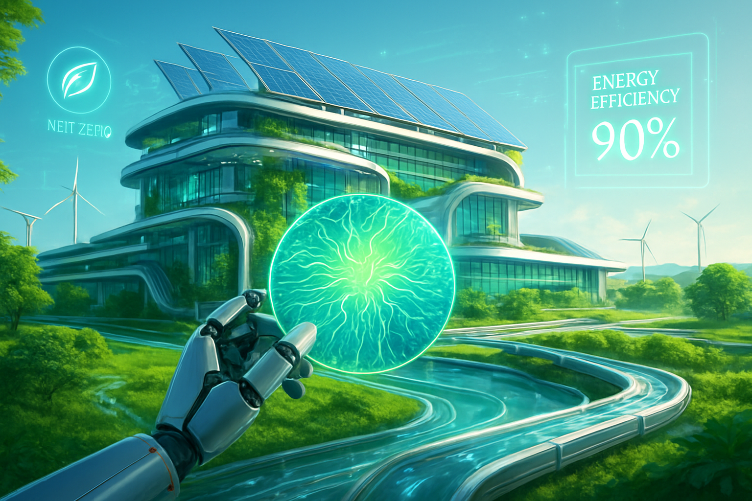
The technical evolution of the 2026 "Green Fab" is defined by a transition toward near-total circularity, specifically in the management of water and chemicals. Modern facilities are now deploying Industrial Water Reclamation Plants (IWRP) that utilize Electrodialysis Reversal (EDR) and Forward Osmosis (FO) to achieve water recycling rates exceeding 90%. Unlike previous generations of "reclamation," which only treated gray water for cooling towers, these 2026 systems can remove dissolved metals like Copper and Manganese down to parts-per-billion levels, allowing the water to be recycled back into the Ultra-Pure Water (UPW) stream required for sensitive lithography steps.
A major breakthrough in early 2026 is the successful transition to PFAS-free chemicals in high-volume manufacturing. While "forever chemicals" were long considered essential for the precision required in EUV (Extreme Ultraviolet) lithography, companies like Fujifilm (OTC: FUJIY) and Central Glass have finally brought commercially viable PFAS-free photoresists to market. These new formulations eliminate per- and polyfluoroalkyl substances while maintaining the high resolution necessary for 2nm nodes. While the industry is still grappling with PFAS-free alternatives for dry etching, new Point-of-Use (POU) Abatement Systems installed in 2026-era fabs can now capture and destroy 99.9% of these emissions before they leave the facility.
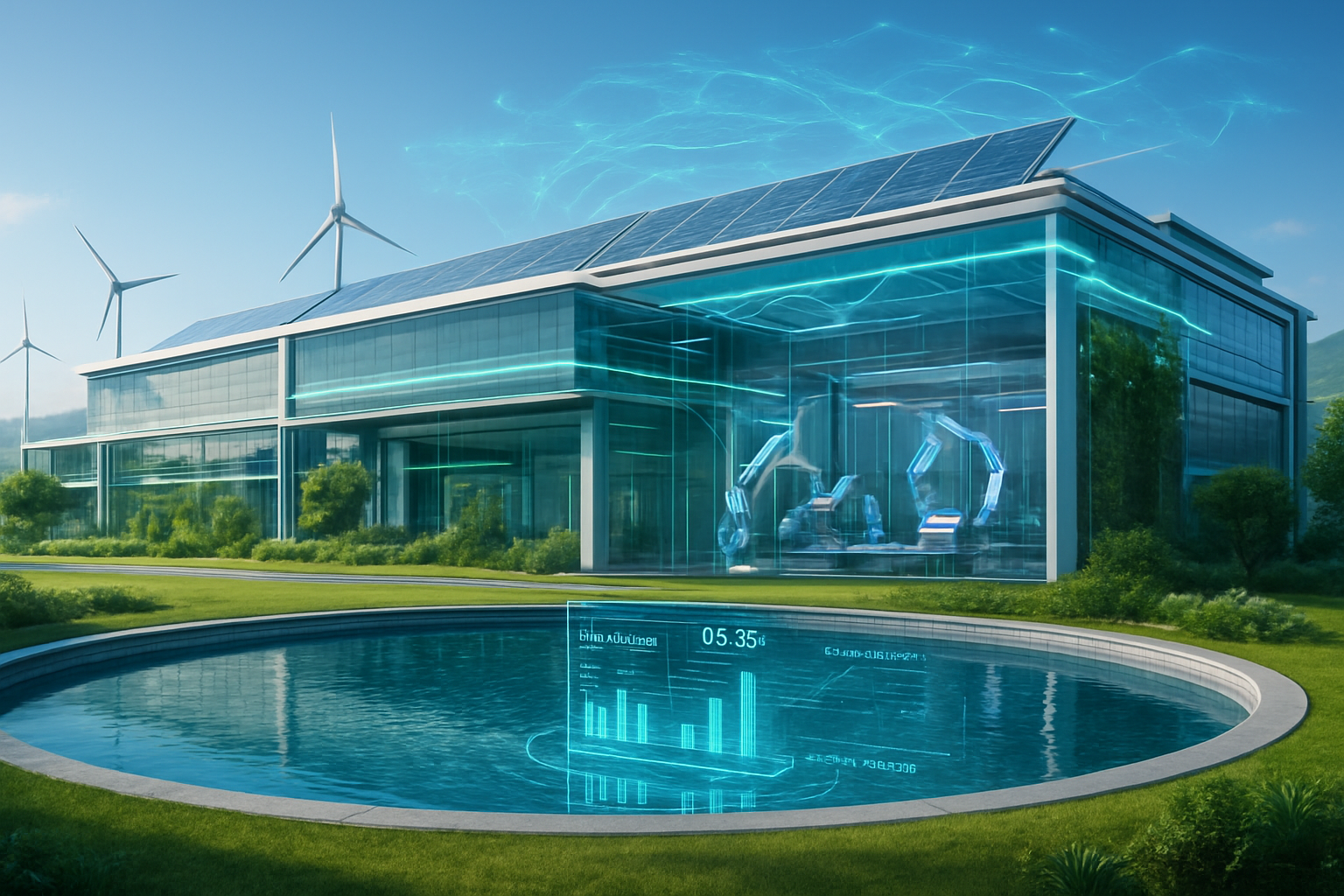
To manage the immense power demands of these "Mega-Fabs," 2026 marks the widespread adoption of AI-driven Digital Twins. Utilizing platforms from Siemens (ETR: SIE) and NVIDIA (NASDAQ: NVDA), plant managers now use real-time 3D replicas of their facilities to simulate "What-If" scenarios. These AI models predict HVAC loads based on external weather patterns and optimize chiller plant efficiency, reducing total energy overhead by up to 20%. This level of optimization allows fabs to function as "prosumers" on the energy grid, using on-site solar arrays and massive battery storage systems to balance the load during peak demand without sacrificing 100% renewable uptime.
The Business of Green Silicon: Winners and the "Green Premium"
The move toward sustainable manufacturing has birthed a new economic reality: the "Green Premium." In early 2026, chips produced in certified carbon-neutral or water-positive facilities carry an estimated price premium of 5% to 15%. However, this cost is being eagerly absorbed by tech giants like Apple (NASDAQ: AAPL) and Microsoft (NASDAQ: MSFT). Apple has reportedly secured nearly 50% of TSMC's 2nm "Green" capacity for 2026, using its high-margin "Pro" and "Ultra" device tiers to insulate consumers from the increased manufacturing costs.
Microsoft, meanwhile, has institutionalized a carbon-neutral supply chain through its Internal Carbon Fee Model. By charging its internal business units (such as Azure and Xbox) for their carbon footprints, Microsoft has created a massive fund to subsidize Green Power Purchase Agreements (PPAs) and invest in carbon removal credits. This strategic positioning gives these tech giants a competitive edge in an era where institutional investors and ESG-conscious consumers demand transparency. Startups and mid-tier chip companies, however, face a tougher challenge, as they lack the capital to invest in the $300 million on-site reclamation plants that define the modern green facility.
The strategic map of the industry is also shifting due to these sustainability demands. While Intel (NASDAQ: INTC) has pushed ahead with its "Silicon Heartland" project in Ohio—featuring a state-funded water reclamation plant—it has officially paused its Magdeburg project in Germany as of February 2026 due to financial restructuring and cooling European demand. This move highlights a growing divergence: the "Green Revolution" is currently most active where government subsidies, like those from the US CHIPS Act, are explicitly tied to environmental milestones.
Regulating the Future: From CSR to Compliance
In 2026, the transition to green fabs has moved beyond voluntary Corporate Social Responsibility (CSR) into the realm of strict regulatory compliance. The US EPA’s TSCA Section 8 reporting deadline passed in January 2026, forcing semiconductor firms to submit a decade's worth of data on PFAS usage. This transparency is now driving a "compliance enforcement" phase where investors can see exactly which companies are lagging in their chemical transitions. In Europe, while the ECHA (European Chemicals Agency) is considering a 13.5-year "essential use" exemption for certain semiconductor processes, the pressure to innovate away from PFAS remains immense.
This regulatory environment is fundamentally different from the 2020-2022 era. The "Green Fab" is now a geopolitical asset. Nations that can provide both the massive power grids required for 2nm production and the renewable energy to back it up are becoming the preferred hubs for the next generation of AI silicon. This has led to a "race to the top" in environmental standards, as countries compete to attract investment by offering "Green Microgrids" and integrated water management infrastructure as part of their industrial incentives.
However, concerns remain regarding the "Scope 3" emissions of the semiconductor industry—the carbon footprint of the entire supply chain, from raw material mining to end-of-life disposal. While the fabs themselves are becoming cleaner, the extraction of rare earth metals remains an environmental bottleneck. To address this, 2026 has seen the rise of "closed-loop agreements," where companies like Apple return end-of-life hardware to recyclers who recover Cobalt and Neodymium, which are then fed back into the manufacturing pipeline, effectively "paying" for new chips with recycled materials.
Looking Ahead: The Autonomous, Prosumer Fab
The next phase of green manufacturing, expected between 2027 and 2030, will likely focus on the complete elimination of fluorinated gases in etching—a feat that has remained the "final frontier" of green chemistry. Researchers are currently pilot-testing "Fluorine, Argon, Nitrogen" (FAN) gas mixtures as non-PFAS alternatives for cleaning and etching, with early results suggesting a potential rollout in late 2027. If successful, this would allow fabs to finally claim a PFAS-free status across the entire manufacturing flow.
Furthermore, the role of the fab in the local community is evolving. Experts predict that by 2028, new fabs will act as central nodes in regional "circular economies," sharing treated wastewater with local agriculture and providing excess heat from cleanrooms to warm local municipal buildings. This "Community-Integrated Fab" model would move the industry from being a resource drain to a resource provider, a shift that will be necessary to gain public approval for the next wave of "Giga-Fabs" planned for the end of the decade.
A New Era for Silicon
The emergence of sustainable "Green" fabs in 2026 represents a landmark achievement in the history of the semiconductor industry. What was once seen as an irreconcilable conflict between the massive resource demands of advanced computing and the need for environmental preservation is being resolved through technical ingenuity and strategic investment. The "Big Three" have proven that 90% water recycling and 100% renewable energy are not just aspirational goals, but operational realities of the modern 2nm and 3nm nodes.
As we look toward the remainder of 2026, the industry’s progress will be measured by its ability to scale these green technologies beyond the flagship "Mega-Fabs" and into the broader global supply chain. The "Silicon Revolution" has officially turned green, and the chips powering the AI era are finally being built with the planet’s future in mind.
This content is intended for informational purposes only and represents analysis of current AI developments.
TokenRing AI delivers enterprise-grade solutions for multi-agent AI workflow orchestration, AI-powered development tools, and seamless remote collaboration platforms.
For more information, visit https://www.tokenring.ai/.