Tag: Hardware Breakthroughs

  • The Optical Revolution: Silicon Photonics Shatters the AI Interconnect Bottleneck

    The Optical Revolution: Silicon Photonics Shatters the AI Interconnect Bottleneck

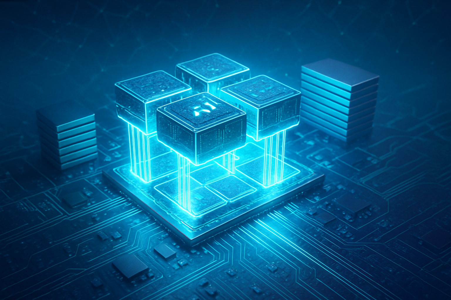
    As of December 18, 2025, the artificial intelligence industry has reached a pivotal inflection point where the speed of light is no longer a theoretical limit, but a production requirement. For years, the industry has warned of a looming "interconnect bottleneck"—a physical wall where the electrical wires connecting GPUs could no longer keep pace with the massive data demands of trillion-parameter models. This week, that wall was officially dismantled as the tech industry fully embraced silicon photonics, shifting the fundamental medium of AI communication from electrons to photons.

    The significance of this transition cannot be overstated. With the recent announcement that Marvell Technology (NASDAQ: MRVL) has finalized its landmark acquisition of Celestial AI for $3.25 billion, the race to integrate "Photonic Fabrics" into the heart of AI silicon has moved from the laboratory to the center of the global supply chain. By replacing copper traces with microscopic lasers and fiber optics, AI clusters are now achieving bandwidth densities and energy efficiencies that were considered impossible just twenty-four months ago, effectively unlocking the next era of "cluster-scale" computing.

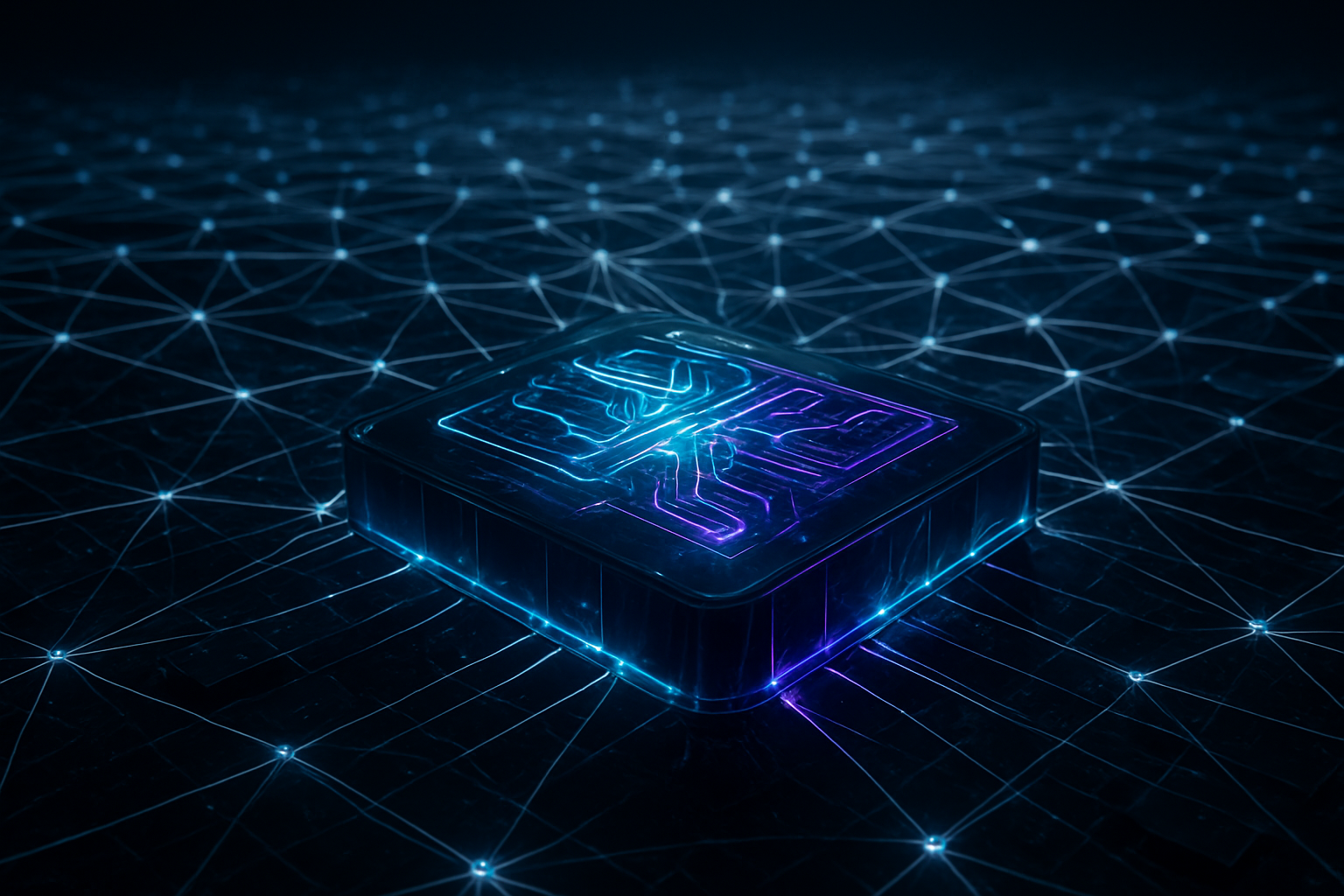
    The End of the Copper Era: Technical Breakthroughs in Optical I/O

    The primary driver behind the shift to silicon photonics is the dual crisis of the "Shoreline Limitation" and the "Power Wall." In traditional GPU architectures, such as the early iterations of the Blackwell series from Nvidia (NASDAQ: NVDA), data must travel through the physical edges (the shoreline) of the chip via electrical pins. As logic density increased, the perimeter of the chip simply ran out of room for more pins. Furthermore, pushing electrical signals through copper at speeds exceeding 200 Gbps requires massive amounts of power for signal retiming. In 2024, nearly 30% of an AI cluster's energy was wasted just moving data between chips; in late 2025, silicon photonics has slashed that "optics tax" by over 80%.

    Technically, this is achieved through Co-Packaged Optics (CPO) and Optical I/O chiplets. Instead of using external pluggable transceivers, companies are now 3D-stacking Photonic Integrated Circuits (PICs) directly onto the GPU or switch die. This allows for "Edgeless I/O," where data can be beamed directly from the center of the chip using light. Leading the charge is Broadcom (NASDAQ: AVGO), which recently began mass-shipping its Tomahawk 6 "Davidson" switch, the industry’s first 102.4 Tbps CPO platform. By integrating optical engines onto the substrate, Broadcom has reduced interconnect power consumption from 30 picojoules per bit (pJ/bit) to less than 5 pJ/bit.

    This shift differs fundamentally from previous networking upgrades. While past transitions moved from 400G to 800G using the same electrical principles, silicon photonics changes the physics of the connection. Startups like Lightmatter have introduced the Passage M1000, a photonic interposer that supports a staggering 114 Tbps of optical bandwidth. This "photonic superchip" allows thousands of individual accelerators to behave as a single, unified processor with near-zero latency, a feat the AI research community has hailed as the most significant hardware breakthrough since the invention of the High Bandwidth Memory (HBM) stack.

    Market Warfare: Who Wins the Photonic Arms Race?

    The competitive landscape of the semiconductor industry is being redrawn by this optical pivot. Nvidia remains the titan to beat, having integrated silicon photonics into its Rubin architecture, slated for wide release in 2026. By leveraging its Spectrum-X networking fabric, Nvidia is moving toward a future where the entire back-end of an AI supercomputer is a seamless web of light. However, the Marvell acquisition of Celestial AI signals a direct challenge to Nvidia’s dominance. Marvell’s new "Photonic Fabric" aims to provide an open, high-bandwidth alternative that allows third-party AI accelerators to compete with Nvidia’s proprietary NVLink on performance and scale.

    Broadcom and Intel (NASDAQ: INTC) are also carving out massive territories in this new market. Broadcom’s lead in CPO technology makes them the indispensable partner for "Hyperscalers" like Google and Meta, who are building custom AI silicon (XPUs) that require optical attaches to scale. Meanwhile, Intel has successfully integrated its Optical Compute Interconnect (OCI) chiplets into its latest Xeon and Gaudi lines. Intel’s milestone of shipping over 8 million PICs demonstrates a manufacturing maturity that many startups still struggle to match, positioning the company as a primary foundry for the photonic era.

    For AI startups and labs, this development is a strategic lifeline. The ability to scale clusters to 100,000+ GPUs without the exponential power costs of copper allows smaller players to train increasingly sophisticated models. However, the high capital expenditure required to transition to optical infrastructure may further consolidate power among the "Big Tech" firms that can afford to rebuild their data centers from the ground up. We are seeing a shift where the "moat" for an AI company is no longer just its algorithm, but the photonic efficiency of its underlying hardware fabric.

    Beyond the Bottleneck: Global and Societal Implications

    The broader significance of silicon photonics extends into the realm of global energy sustainability. As AI energy consumption became a flashpoint for environmental concerns in 2024 and 2025, the move to light-based communication offers a rare "green" win for the industry. By reducing the energy required for data movement by 5x to 10x, silicon photonics is the primary reason the tech industry can continue to scale AI capabilities without triggering a collapse of local power grids. It represents a decoupling of performance growth from energy growth.

    Furthermore, this technology is the key to achieving "Disaggregated Memory." In the electrical era, a GPU could only efficiently access the memory physically located on its board. With the low latency and long reach of light, 2025-era data centers are moving toward pools of memory that can be dynamically assigned to any processor in the rack. This "memory-centric" computing model is essential for the next generation of Large Multimodal Models (LMMs) that require petabytes of active memory to process real-time video and complex reasoning tasks.

    However, the transition is not without its concerns. The reliance on silicon photonics introduces new complexities in the supply chain, particularly regarding the manufacturing of high-reliability lasers. Unlike traditional silicon, these lasers are often made from III-V materials like Indium Phosphide, which are more difficult to integrate and have different failure modes. There is also a geopolitical dimension; as silicon photonics becomes the "secret sauce" of AI supremacy, export controls on photonic design software and manufacturing equipment are expected to tighten, mirroring the restrictions seen in the EUV lithography market.

    The Road Ahead: What’s Next for Optical Computing?

    Looking toward 2026 and 2027, the industry is already eyeing the next frontier: all-optical computing. While silicon photonics currently handles the communication between chips, companies like Ayar Labs and Lightmatter are researching ways to perform certain computations using light itself. This would involve optical matrix-vector multipliers that could process neural network layers at the speed of light with almost zero heat generation. While still in the early stages, the success of optical I/O has provided the commercial foundation for these more radical architectures.

    In the near term, expect to see the "UCIe (Universal Chiplet Interconnect Express) over Light" standard become the dominant protocol for chip-to-chip communication. This will allow a "Lego-like" ecosystem where a customer can pair an Nvidia GPU with a Marvell photonic chiplet and an Intel memory controller, all communicating over a standardized optical bus. The main challenge remains the "yield" of these complex 3D-stacked packages; as manufacturing processes mature throughout 2026, we expect the cost of optical I/O to drop, eventually making it standard even in consumer-grade edge AI devices.

    Experts predict that by 2028, the term "interconnect bottleneck" will be a relic of the past. The focus will shift from how to move data to how to manage the sheer volume of intelligence that these light-speed clusters can generate. The "Optical Era" of AI is not just about faster chips; it is about the creation of a global, light-based neural fabric that can sustain the computational demands of Artificial General Intelligence (AGI).

    A New Foundation for the Intelligence Age

    The transition to silicon photonics marks the end of the "Electrical Bottleneck" that has constrained computer architecture since the 1940s. By successfully replacing copper with light, the AI industry has bypassed a physical limit that many feared would stall the progress of machine intelligence. The developments we have witnessed in late 2025—from Marvell’s strategic acquisitions to Broadcom’s record-breaking switches—confirm that the future of AI is optical.

    As we look forward, the significance of this milestone will likely be compared to the transition from vacuum tubes to transistors. It is a fundamental shift in the physics of information. While the challenges of laser reliability and manufacturing costs remain, the momentum is irreversible. For the coming months, keep a close watch on the deployment of "Rubin" systems and the first wave of 100-Tbps optical switches; these will be the yardsticks by which we measure the success of the photonic revolution.


    This content is intended for informational purposes only and represents analysis of current AI developments.

    TokenRing AI delivers enterprise-grade solutions for multi-agent AI workflow orchestration, AI-powered development tools, and seamless remote collaboration platforms.
    For more information, visit https://www.tokenring.ai/.

  • Breaking the Memory Wall: Eliyan’s Modular Interconnects Revolutionize AI Chip Design

    Breaking the Memory Wall: Eliyan’s Modular Interconnects Revolutionize AI Chip Design

    Eliyan's innovative NuLink and NuLink-X PHY (physical layer) solutions are poised to fundamentally transform AI chip design by reinventing chip-to-chip and die-to-die connectivity. This groundbreaking modular semiconductor technology directly addresses critical bottlenecks in generative AI systems, offering unprecedented bandwidth, significantly lower power consumption, and enhanced design flexibility. Crucially, it achieves this high-performance interconnectivity on standard organic substrates, moving beyond the limitations and expense of traditional silicon interposers. This development arrives at a pivotal moment, as the explosive growth of generative AI and large language models (LLMs) places immense and escalating demands on computational resources and high-bandwidth memory, making efficient data movement more critical than ever.

    The immediate significance of Eliyan's technology lies in its ability to dramatically increase the memory capacity and performance of HBM-equipped GPUs and ASICs, which are the backbone of modern AI infrastructure. By enabling advanced-packaging-like performance on more accessible and cost-effective organic substrates, Eliyan reduces the overall cost and complexity of high-performance multi-chiplet designs. Furthermore, its focus on power efficiency is vital for the energy-intensive AI data centers, contributing to more sustainable AI development. By tackling the pervasive "memory wall" problem and the inherent limitations of monolithic chip designs, Eliyan is set to accelerate the development of more powerful, efficient, and economically viable AI chips, democratizing chiplet adoption across the tech industry.

    Technical Deep Dive: Unpacking Eliyan's NuLink Innovation

    Eliyan's modular semiconductor technology, primarily its NuLink and NuLink-X PHY solutions, represents a significant leap forward in chiplet interconnects. At its core, NuLink PHY is a high-speed serial die-to-die (D2D) interconnect, while NuLink-X extends this capability to chip-to-chip (C2C) connections over longer distances on a Printed Circuit Board (PCB). The technology boasts impressive specifications, with the NuLink-2.0 PHY, demonstrated on a 3nm process, achieving an industry-leading 64Gbps/bump. An earlier 5nm implementation showed 40Gbps/bump. This translates to a remarkable bandwidth density of up to 4.55 Tbps/mm in standard organic packaging and an even higher 21 Tbps/mm in advanced packaging.

    A key differentiator is Eliyan's patented Simultaneous Bidirectional (SBD) signaling technology. SBD allows data to be transmitted and received on the same wire concurrently, effectively doubling the bandwidth per interface. This, coupled with ultra-low power consumption (less than half a picojoule per bit and approximately 30% of the power of advanced packaging solutions), provides a significant advantage for power-hungry AI workloads. Furthermore, the technology is protocol-agnostic, supporting industry standards like Universal Chiplet Interconnect Express (UCIe) and Bunch of Wires (BoW), ensuring broad compatibility within the emerging chiplet ecosystem. Eliyan also offers NuGear chiplets, which act as adapters to convert HBM (High Bandwidth Memory) PHY interfaces to NuLink PHY, facilitating the integration of standard HBM parts with GPUs and ASICs over organic substrates.

    Eliyan's approach fundamentally differs from traditional interconnects and silicon interposers by delivering silicon-interposer-class performance on cost-effective, robust organic substrates. This innovation bypasses the need for expensive and complex silicon interposers in many applications, broadening access to high-bandwidth die-to-die links beyond proprietary advanced packaging flows like Taiwan Semiconductor Manufacturing Company (NYSE: TSM) TSMC's CoWoS. This shift significantly reduces packaging, assembly, and testing costs by at least 2x, while also mitigating supply chain risks due to the wider availability of organic substrates. Initial reactions from the AI research community and industry experts have been overwhelmingly positive, with comments highlighting its ability to "double the bandwidth at less than half the power consumption" and its potential to "rewrite how chiplets come together," as noted by Raja Koduri, Founder and CEO of Mihira AI. Eliyan's strong industry backing, including strategic investments from major HBM suppliers like Samsung (KRX: 005930), SK Hynix (KRX: 000660), and Micron Technology (NASDAQ: MU), further underscores its transformative potential.

    Industry Impact: Reshaping the AI Hardware Landscape

    Eliyan's modular semiconductor technology is set to create significant ripples across the semiconductor and AI industries, offering profound benefits and competitive shifts. AI chip designers, including industry giants like NVIDIA Corporation (NASDAQ: NVDA), Intel Corporation (NASDAQ: INTC), and Advanced Micro Devices (NASDAQ: AMD), stand to gain immensely. By licensing Eliyan's NuLink IP or integrating its NuGear chiplets, these companies can overcome the performance limitations and size constraints of traditional packaging, enabling higher-performance AI and HPC Systems-on-Chip (SoCs) with significantly increased memory capacity – potentially doubling HBM stacks to 160GB or more for GPUs. This directly translates to superior performance for memory-intensive generative AI inference and training.

    Hyperscalers, such as Alphabet Inc.'s (NASDAQ: GOOGL) Google and other custom AI ASIC designers, are also major near-term beneficiaries. Eliyan's technology allows them to integrate more HBM stacks and compute dies, pushing the boundaries of HBM packaging and maximizing bandwidth density without requiring specialized PHY expertise. Foundries, including TSMC and Samsung Foundry, are also key stakeholders, with Eliyan's technology being "backed by every major HBM and Foundry." Eliyan has demonstrated its NuLink PHY on TSMC's N3 process and is porting it to Samsung Foundry's SF4X process node, indicating broad manufacturing support and offering diverse options for multi-die integration.

    The competitive implications are substantial. Eliyan's technology reduces the industry's dependence on proprietary advanced packaging monopolies, offering a cost-effective alternative to solutions like TSMC's CoWoS. This democratization of chiplet technology lowers cost and complexity barriers, enabling a broader range of companies to innovate in high-performance AI and HPC solutions. While major players have internal interconnect efforts, Eliyan's proven IP offers an accelerated path to market and immediate performance gains. This innovation could disrupt existing advanced packaging paradigms, as it challenges the absolute necessity of silicon interposers for achieving top-tier chiplet performance in many applications, potentially redirecting demand or altering cost-benefit analyses. Eliyan's strategic advantages include its interposer-class performance on organic substrates, patented Simultaneous Bidirectional (SBD) signaling, protocol-agnostic design, and comprehensive solutions that include both IP cores and adapter chiplets, positioning it as a critical enabler for the massive connectivity and memory needs of the generative AI era.

    Wider Significance: A New Era for AI Hardware Scaling

    Eliyan's modular semiconductor technology represents a foundational shift in how AI hardware is designed and scaled, seamlessly integrating with and accelerating the broader trends of chiplets and the explosive growth of generative AI. By enabling high-performance, low-power, and low-latency communication between chips and chiplets on standard organic substrates, Eliyan is a direct enabler for the chiplet ecosystem, making multi-die architectures more accessible and cost-effective. The technology's compatibility with standards like UCIe and BoW, coupled with Eliyan's active contributions to these specifications, solidifies its role as a key building block for open, multi-vendor chiplet platforms. This democratization of chiplet adoption allows for the creation of larger, more complex Systems-in-Package (SiP) solutions that can exceed the size limitations of traditional silicon interposers.

    For generative AI, Eliyan's impact is particularly profound. These models, exemplified by LLMs, are intensely memory-bound, encountering a "memory wall" where processor performance outstrips memory access speeds. Eliyan's NuLink technology directly addresses this by significantly increasing memory capacity and bandwidth for HBM-equipped GPUs and ASICs. For instance, it can potentially double the number of HBMs in a package, from 80GB to 160GB on an NVIDIA A100-like GPU, which could triple AI training performance for memory-intensive applications. This capability is crucial not only for training but, perhaps even more critically, for the inference costs of generative AI, which can be astronomically higher than traditional search queries. By providing higher performance and lower power consumption, Eliyan's NuLink helps data centers keep pace with the accelerating compute loads driven by AI.

    The broader impacts on AI development include accelerated AI performance and efficiency, reduced costs, and increased accessibility to advanced AI capabilities beyond hyperscalers. The enhanced design flexibility and customization offered by modular, protocol-agnostic interconnects are essential for creating specialized AI chips tailored to specific workloads. Furthermore, the improved compute efficiency and potential for simplified compute clusters contribute to greater sustainability in AI, aligning with green computing initiatives. While promising, potential concerns include adoption challenges, given the inertia of established solutions, and the creation of new dependencies on Eliyan's IP. However, Eliyan's compatibility with open standards and strong industry backing are strategic moves to mitigate these issues. Compared to previous AI hardware milestones, such as the GPU revolution led by NVIDIA (NASDAQ: NVDA) CUDA and Tensor Cores, or Google's (NASDAQ: GOOGL) custom TPUs, Eliyan's technology complements these advancements by addressing the critical challenge of efficient, high-bandwidth data movement between computational cores and memory in modular systems, enabling the continued scaling of AI at a time when monolithic chip designs are reaching their limits.

    Future Developments: The Horizon of Modular AI

    The trajectory for Eliyan's modular semiconductor technology and the broader chiplet ecosystem points towards a future defined by increased modularity, performance, and accessibility. In the near term, Eliyan is set to push the boundaries of bandwidth and power efficiency further. The successful demonstration of its NuLink-2.0 PHY in a 3nm process, achieving 64Gbps/bump, signifies a continuous drive for higher performance. A critical focus remains on leveraging standard organic/laminate packaging to achieve high performance, making chiplet designs more cost-effective and suitable for a wider range of applications, including industrial and automotive sectors where reliability is paramount. Eliyan is also actively addressing the "memory wall" by enabling HBM3-like memory bandwidth on standard packaging and developing Universal Memory Interconnect (UMI) to improve Die-to-Memory bandwidth efficiency, with specifications being finalized as BoW 2.1 with the Open Compute Project (OCP).

    Long-term, chiplets are projected to become the dominant approach to chip design, offering unprecedented flexibility and performance. The vision includes open, multi-vendor chiplet packages, where components from different suppliers can be seamlessly integrated, heavily reliant on the widespread adoption of standards like UCIe. Eliyan's contributions to these open standards are crucial for fostering this ecosystem. Experts predict the emergence of trillion-transistor packages featuring stacked CPUs, GPUs, and memory, with Eliyan's advancements in memory interconnect and multi-die integration being indispensable for such high-density, high-performance systems. Specialized acceleration through domain-specific chiplets for tasks like AI inference and cryptography will also become prevalent, allowing for highly customized and efficient AI hardware.

    Potential applications on the horizon span across AI and High-Performance Computing (HPC), data centers, automotive, mobile, and edge computing. In AI and HPC, chiplets will be critical for meeting the escalating demands for memory and computing power, enabling large-scale integration and modular designs optimized for energy efficiency. The automotive sector, particularly with ADAS and autonomous vehicles, presents a significant opportunity for specialized chiplets integrating sensors and AI processing units, where Eliyan's standard packaging solutions offer enhanced reliability. Despite the immense potential, challenges remain, including the need for fully mature and universally adopted interconnect standards, gaps in electronic design automation (EDA) toolchains for complex multi-die systems, and sophisticated thermal management for densely packed chiplets. However, experts predict that 2025 will be a "tipping point" for chiplet adoption, driven by maturing standards and AI's insatiable demand for compute. The chiplet market is poised for explosive growth, with projections reaching US$411 billion by 2035, underscoring the transformative role Eliyan is set to play.

    Wrap-Up: Eliyan's Enduring Legacy in AI Hardware

    Eliyan's modular semiconductor technology, spearheaded by its NuLink™ PHY and NuGear™ chiplets, marks a pivotal moment in the evolution of AI hardware. The key takeaway is its ability to deliver industry-leading high-performance, low-power die-to-die and chip-to-chip interconnectivity on standard organic packaging, effectively bypassing the complexities and costs associated with traditional silicon interposers. This innovation, bolstered by patented Simultaneous Bidirectional (SBD) signaling and compatibility with open standards like UCIe and BoW, significantly enhances bandwidth density and reduces power consumption, directly addressing the "memory wall" bottleneck that plagues modern AI systems. By providing NuGear chiplets that enable standard HBM integration with organic substrates, Eliyan democratizes access to advanced multi-die architectures, making high-performance AI more accessible and cost-effective.

    Eliyan's significance in AI history is profound, as it provides a foundational solution for scalable and efficient AI systems in an era where generative AI models demand unprecedented computational and memory resources. Its technology is a critical enabler for accelerating AI performance, reducing costs, and fostering greater design flexibility, which are essential for the continued progress of machine learning. The long-term impact on the AI and semiconductor industries will be transformative: diversified supply chains, reduced manufacturing costs, sustained performance scaling for AI as models grow, and the acceleration of a truly open and interoperable chiplet ecosystem. Eliyan's active role in shaping standards, such as OCP's BoW 2.0/2.1 for HBM integration, solidifies its position as a key architect of future AI infrastructure.

    As we look ahead, several developments bear watching in the coming weeks and months. Keep an eye out for commercialization announcements and design wins from Eliyan, particularly with major AI chip developers and hyperscalers. Further developments in standard specifications with the OCP, especially regarding HBM4 integration, will define future memory-intensive AI and HPC architectures. The expansion of Eliyan's foundry and process node support, building on its successful tape-outs with TSMC (NYSE: TSM) and ongoing work with Samsung Foundry (KRX: 005930), will indicate its broadening market reach. Finally, strategic partnerships and product line expansions beyond D2D interconnects to include D2M (die-to-memory) and C2C (chip-to-chip) solutions will showcase the full breadth of Eliyan's market strategy and its enduring influence on the future of AI and high-performance computing.


    This content is intended for informational purposes only and represents analysis of current AI developments.

    TokenRing AI delivers enterprise-grade solutions for multi-agent AI workflow orchestration, AI-powered development tools, and seamless remote collaboration platforms.
    For more information, visit https://www.tokenring.ai/.