Tag: Hardware Innovation

  • The Nanosheet Revolution: TSMC Commences Volume Production of 2nm Chips to Power the AI Supercycle

    The Nanosheet Revolution: TSMC Commences Volume Production of 2nm Chips to Power the AI Supercycle

    As of January 12, 2026, the global semiconductor landscape has officially entered its most transformative era in over a decade. Taiwan Semiconductor Manufacturing Company (NYSE:TSM / TPE:2330), the world’s largest contract chipmaker, has confirmed that its 2-nanometer (N2) process node is now in high-volume manufacturing (HVM). This milestone marks the end of the "FinFET" transistor era and the beginning of the "Nanosheet" era, providing the essential hardware foundation for the next generation of generative AI models, autonomous systems, and ultra-efficient mobile devices.

    The shift to 2nm is more than a incremental upgrade; it is a fundamental architectural pivot designed to overcome the "power wall" that has threatened to stall AI progress. By delivering a staggering 30% reduction in power consumption compared to current 3nm technologies, TSMC is enabling a future where massive Large Language Models (LLMs) can run with significantly lower energy footprints. This announcement solidifies TSMC’s dominance in the foundry market, as the company scales production to meet the insatiable demand from the world's leading technology giants.

    The Technical Leap: From Fins to Nanosheets

    The core of the N2 node’s success lies in the transition from FinFET (Fin Field-Effect Transistor) to Gate-All-Around (GAA) Nanosheet transistors. For nearly 15 years, FinFET served the industry well, but as transistors shrunk toward the atomic scale, current leakage became an insurmountable hurdle. The Nanosheet design solves this by stacking horizontal layers of silicon and surrounding them on all four sides with the gate. This 360-degree control virtually eliminates leakage, allowing for tighter electrostatic management and drastically improved energy efficiency.

    Technically, the N2 node offers a "full-node" leap over the previous N3E (3nm) process. According to TSMC’s engineering data, the 2nm process delivers a 10% to 15% performance boost at the same power level, or a 25% to 30% reduction in power consumption at the same clock speed. Furthermore, TSMC has introduced a proprietary technology called Nano-Flex™. This allows chip designers to mix and match nanosheets of different heights within a single block—using "tall" nanosheets for high-performance compute cores and "short" nanosheets for energy-efficient background tasks. This level of granularity is unprecedented and gives designers a new toolkit for balancing the thermal and performance needs of complex AI silicon.

    Initial reports from the Hsinchu and Kaohsiung fabs indicate that yield rates for the N2 node are remarkably mature, sitting between 65% and 75%. This is a significant achievement for a first-generation architectural shift, as new nodes typically struggle to reach such stability in their first few months of volume production. The integration of "Super-High-Performance Metal-Insulator-Metal" (SHPMIM) capacitors further enhances the node, providing double the capacitance density and a 50% reduction in resistance, which ensures stable power delivery for the high-frequency bursts required by AI inference engines.

    The Industry Impact: Securing the AI Supply Chain

    The commencement of 2nm production has sparked a gold rush among tech titans. Apple (NASDAQ:AAPL) has reportedly secured over 50% of TSMC’s initial N2 capacity through 2026. The upcoming A20 Pro chip, expected to power the next generation of iPhones and iPads, will likely be the first consumer-facing product to utilize this technology, giving Apple a significant lead in on-device "Edge AI" capabilities. Meanwhile, NVIDIA (NASDAQ:NVDA) and AMD (NASDAQ:AMD) are racing to port their next-generation AI accelerators to the N2 node. NVIDIA’s rumored "Vera Rubin" architecture and AMD’s "Venice" EPYC processors are expected to leverage the 2nm efficiency to pack more CUDA and Zen cores into the same thermal envelope.

    The competitive landscape is also shifting. While Samsung (KRX:005930) was technically the first to move to GAA at the 3nm stage, it has struggled with yield issues, leading many major customers to remain with TSMC for the 2nm transition. Intel (NASDAQ:INTC) remains the most aggressive challenger with its 18A node, which includes "PowerVia" (back-side power delivery) ahead of TSMC’s roadmap. However, industry analysts suggest that TSMC’s manufacturing scale and "yield learning curve" give it a massive commercial advantage. Hyperscalers like Amazon (NASDAQ:AMZN), Alphabet/Google (NASDAQ:GOOGL), and Microsoft (NASDAQ:MSFT) are also lining up for N2 capacity to build custom AI ASICs, aiming to reduce their reliance on off-the-shelf hardware and lower the massive electricity bills associated with their data centers.

    The Broader Significance: Breaking the Power Wall

    The arrival of 2nm silicon comes at a critical juncture for the AI industry. As LLMs move toward tens of trillions of parameters, the environmental and economic costs of training and running these models have become a primary concern. The 30% power reduction offered by N2 acts as a "pressure release valve" for the global energy grid. By allowing for more "tokens per watt," the 2nm node enables the scaling of generative AI without a linear increase in carbon emissions or infrastructure costs.

    Furthermore, this development accelerates the rise of "Physical AI" and robotics. For an autonomous robot or a self-driving car to process complex visual data in real-time, it requires massive compute power within a limited battery and thermal budget. The efficiency of Nanosheet transistors makes these applications more viable, moving AI from the cloud to the physical world. However, the transition is not without its hurdles. The cost of 2nm wafers is estimated to be between $25,000 and $30,000, a 50% increase over 3nm. This "silicon inflation" may widen the gap between the tech giants who can afford the latest nodes and smaller startups that may be forced to rely on older, less efficient hardware.

    Future Horizons: The Path to 1nm and Beyond

    TSMC’s roadmap does not stop at N2. The company has already outlined plans for N2P, an enhanced version of the 2nm node, followed by the A16 (1.6nm) node in late 2026. The A16 node will be the first to feature "Super Power Rail," TSMC’s version of back-side power delivery, which moves power wiring to the underside of the wafer to free up more space for signal routing. Beyond that, the A14 (1.4nm) and A10 (1nm) nodes are already in the research and development phase, with the latter expected to explore new materials like 2D semiconductors to replace traditional silicon.

    One of the most watched developments will be TSMC’s adoption of High-NA EUV lithography machines from ASML (NASDAQ:ASML). While Intel has already begun using these $380 million machines, TSMC is taking a more conservative approach, opting to stick with existing Low-NA EUV for the initial N2 ramp-up to keep costs manageable and yields high. This strategic divergence between the two semiconductor giants will likely determine the leadership of the foundry market for the remainder of the decade.

    A New Chapter in Computing History

    The official start of volume production for TSMC’s 2nm process is a watershed moment in computing history. It represents the successful navigation of one of the most difficult engineering transitions the industry has ever faced. By mastering the Nanosheet architecture, TSMC has ensured that Moore’s Law—or at least its spirit—continues to drive the AI revolution forward. The immediate significance lies in the massive efficiency gains that will soon be felt in everything from flagship smartphones to the world’s most powerful supercomputers.

    In the coming months, the industry will be watching closely for the first third-party benchmarks of 2nm silicon. As the first chips roll off the assembly lines in Taiwan and head to packaging facilities, the true impact of the Nanosheet era will begin to materialize. For now, TSMC has once again proven that it is the indispensable linchpin of the global technology ecosystem, providing the literal foundation upon which the future of artificial intelligence is being built.


    This content is intended for informational purposes only and represents analysis of current AI developments.

    TokenRing AI delivers enterprise-grade solutions for multi-agent AI workflow orchestration, AI-powered development tools, and seamless remote collaboration platforms.
    For more information, visit https://www.tokenring.ai/.

  • The Silicon Brain: How Next-Gen AI Chips Are Rewriting the Future of Intelligence

    The Silicon Brain: How Next-Gen AI Chips Are Rewriting the Future of Intelligence

    The artificial intelligence revolution, once primarily a software-driven phenomenon, is now being fundamentally reshaped by a parallel transformation in hardware. As traditional processors hit their architectural limits, a new era of AI chip architecture is dawning. This shift is characterized by innovative designs and specialized accelerators that promise to unlock unprecedented AI capabilities with immediate and profound impact, moving beyond the general-purpose computing paradigms that have long dominated the tech landscape. These advancements are not just making AI faster; they are making it smarter, more efficient, and capable of operating in ways previously thought impossible, signaling a critical juncture in the development of artificial intelligence.

    Unpacking the Architectural Revolution: Specialized Silicon for a Smarter Future

    The future of AI chip architecture is rapidly evolving, driven by the increasing demand for computational power, energy efficiency, and real-time processing required by complex AI models. This evolution is moving beyond traditional CPU and GPU architectures towards specialized accelerators and innovative designs, with the global AI hardware market projected to reach $210.50 billion by 2034. Experts believe that the next phase of AI breakthroughs will be defined by hardware innovation, not solely by larger software models, prioritizing faster, more efficient, and scalable chips, often adopting multi-component, heterogeneous systems where each component is engineered for a specific function within a single package.

    At the forefront of this revolution are groundbreaking designs that fundamentally rethink how computation and memory interact. Neuromorphic computing, for instance, draws inspiration from the human brain, utilizing "spiking neural networks" (SNNs) to process information. Unlike traditional processors that execute instructions sequentially or in parallel with predefined instructions, these chips are event-driven, activating only when new information is detected, much like biological neurons communicate through discrete electrical spikes. This brain-inspired approach, exemplified by Intel (NASDAQ: INTC)'s Hala Point, which uses over 1,000 Loihi 2 processors, offers exceptional energy efficiency, real-time processing, and adaptability, enabling AI to learn dynamically on the device. Initial prototypes have shown performing AI workloads 50 times faster and using 100 times less energy than conventional systems.

    Another significant innovation is In-Memory Computing (IMC), which directly tackles the "von Neumann bottleneck"—the inefficiency caused by data constantly shuffling between the processor and separate memory units. IMC integrates computation directly within or adjacent to memory units, drastically reducing data transfer delays and power consumption. This approach is particularly promising for large AI models and compact edge devices, offering significant improvements in AI costs, reduced compute time, and lower power usage, especially for inference applications. Complementing this, 3D Stacking (or 3D packaging) involves vertically integrating multiple semiconductor dies. This allows for massive and fast data movement by shortening interconnect distances, bypassing bottlenecks inherent in flat, 2D designs, and offering substantial improvements in performance and energy efficiency. Companies like AMD (NASDAQ: AMD) with its 3D V-Cache and Intel (NASDAQ: INTC) with Foveros technology are already implementing these advancements, with early prototypes demonstrating performance gains of roughly an order of magnitude over comparable 2D chips.

    These innovative designs are coupled with a new generation of specialized AI accelerators. While Graphics Processing Units (GPUs) from NVIDIA (NASDAQ: NVDA) were revolutionary for parallel AI workloads, dedicated AI chips are taking specialization to the next level. Neural Processing Units (NPUs) are specifically engineered from the ground up for neural network computations, delivering superior performance and energy efficiency, especially for edge computing. Google (NASDAQ: GOOGL)'s Tensor Processing Units (TPUs) are a prime example of custom Application-Specific Integrated Circuits (ASICs), meticulously designed for machine learning tasks. TPUs, now in their seventh generation (Ironwood), feature systolic array architectures and high-bandwidth memory (HBM), capable of performing 16K multiply-accumulate operations per cycle in their latest versions, significantly accelerating AI workloads across Google services. Custom ASICs offer the highest level of optimization, often delivering 10 to 100 times greater energy efficiency compared to GPUs for specific AI tasks, although they come with less flexibility and higher initial design costs. The AI research community and industry experts widely acknowledge the critical role of this specialized hardware, recognizing that future AI breakthroughs will increasingly depend on such infrastructure, not solely on software advancements.

    Reshaping the Corporate Landscape: Who Wins in the AI Silicon Race?

    The advent of advanced AI chip architectures is profoundly impacting the competitive landscape across AI companies, tech giants, and startups, driving a strategic shift towards vertical integration and specialized solutions. This silicon arms race is poised to redefine market leadership and disrupt existing product and service offerings.

    Tech giants are strategically positioned to benefit immensely due to their vast resources and established ecosystems. Companies like Google (NASDAQ: GOOGL), Amazon (NASDAQ: AMZN), Microsoft (NASDAQ: MSFT), and Meta (NASDAQ: META) are heavily investing in developing their own custom AI silicon. Google's TPUs, Amazon Web Services (AWS)'s Trainium and Inferentia chips, Microsoft's Azure Maia 100 and Azure Cobalt 100, and Meta's MTIA are all examples of this vertical integration strategy. By designing their own chips, these companies aim to optimize performance for specific workloads, reduce reliance on third-party suppliers like NVIDIA (NASDAQ: NVDA), and achieve significant cost efficiencies, particularly for AI inference tasks. This move allows them to differentiate their cloud offerings and internal AI services, gaining tighter control over their hardware and software stacks.

    The competitive implications for major AI labs and tech companies are substantial. There's a clear trend towards reduced dependence on NVIDIA's dominant GPUs, especially for AI inference, where custom ASICs can offer lower power consumption and cost. This doesn't mean NVIDIA is out of the game; they continue to lead the AI training market and are exploring advanced packaging like 3D stacking and silicon photonics. However, the rise of custom silicon forces NVIDIA and AMD (NASDAQ: AMD), which is expanding its AI capabilities with products like the MI300 series, to innovate rapidly and offer more specialized, high-performance solutions. The ability to offer AI solutions with superior energy efficiency and lower latency will be a key differentiator, with neuromorphic and in-memory computing excelling in this regard, particularly for edge devices where power constraints are critical.

    This architectural shift also brings potential disruption to existing products and services. The enhanced efficiency of neuromorphic computing, in-memory computing, and NPUs enables more powerful AI processing directly on devices, reducing the need for constant cloud connectivity. This could disrupt cloud-based AI service models, especially for real-time, privacy-sensitive, or low-power applications. Conversely, it could also lead to the democratization of AI, lowering the barrier to entry for AI development by making sophisticated AI systems more accessible and cost-effective. The focus will shift from general-purpose computing to workload-specific optimization, with systems integrating multiple processor types (GPUs, CPUs, NPUs, TPUs) for different tasks, potentially disrupting traditional hardware sales models.

    For startups, this specialized landscape presents both challenges and opportunities. Startups focused on niche hardware or specific AI applications can thrive by providing highly optimized solutions that fill gaps left by general-purpose hardware. For instance, neuromorphic computing startups like BrainChip, Rain Neuromorphics, and GrAI Matter Labs are developing energy-efficient chips for edge AI, robotics, and smart sensors. Similarly, in-memory computing startups like TensorChip and Axelera AI are creating chips for high throughput and low latency at the edge. Semiconductor foundries like TSMC (NYSE: TSM) and Samsung (KRX: 005930), along with IP providers like Marvell (NASDAQ: MRVL) and Broadcom (NASDAQ: AVGO), are crucial enablers, providing the advanced manufacturing and design expertise necessary for these complex architectures. Their mastery of 3D stacking and other advanced packaging techniques will make them essential partners and leaders in delivering the next generation of high-performance AI chips.

    A Broader Canvas: AI Chips and the Future of Society

    The future of AI chip architecture is not just a technical evolution; it's a societal one, deeply intertwined with the broader AI landscape and trends. These advancements are poised to enable unprecedented levels of performance, efficiency, and capability, promising profound impacts across society and various industries, while also presenting significant concerns that demand careful consideration.

    These advanced chip architectures directly address the escalating computational demands and inefficiencies of modern AI. The "memory wall" in traditional von Neumann architectures and the skyrocketing energy costs of training large AI models are major concerns that specialized chips are designed to overcome. The shift towards these architectures signifies a move towards more pervasive, responsive, and efficient intelligence, enabling the proliferation of AI at the "edge"—on devices like IoT sensors, smartphones, and autonomous vehicles—where real-time processing, low power consumption, and data security are paramount. This decentralization of AI capabilities is a significant trend, comparable to the shift from mainframes to personal computing or the rise of cloud computing, democratizing access to powerful computational resources.

    The impacts on society and industries are expected to be transformative. In healthcare, faster and more accurate AI processing will enable early disease diagnosis, personalized medicine, and accessible telemedicine. Autonomous vehicles, drones, and advanced robotics will benefit from real-time decision-making, enhancing safety and efficiency. Cybersecurity will see neuromorphic chips continuously learning from network traffic patterns to detect new and evolving threats with low latency. In manufacturing, advanced robots and optimized industrial processes will become more adaptable and efficient. For consumer electronics, supercomputer-level performance could be integrated into compact devices, powering highly responsive AI assistants and advanced functionalities. Crucially, improved efficiency and reduced power consumption in data centers will be critical for scaling AI operations, leading to lower operational costs and potentially making AI solutions more accessible to developers with limited resources.

    Despite the immense potential, the future of AI chip architecture raises several critical concerns. While newer architectures aim for significant energy efficiency, the sheer scale of AI development still demands immense computational resources, contributing to a growing carbon footprint and straining power grids. This raises ethical questions about the environmental impact and the perpetuation of societal inequalities if AI development is not powered by renewable sources or if biased models are deployed. Ensuring ethical AI development requires addressing issues like data quality, fairness, and the potential for algorithmic bias. The increased processing of sensitive data at the edge also raises privacy concerns that must be managed through secure enclaves and robust data protection. Furthermore, the high cost of developing and deploying high-performance AI accelerators could create a digital divide, although advancements in AI-driven chip design could eventually reduce costs. Other challenges include thermal management for densely packed 3D-stacked chips, the need for new software compatibility and development frameworks, and the rapid iteration of hardware contributing to e-waste.

    This architectural evolution is as significant as, if not more profound than, previous AI milestones. The initial AI revolution was fueled by the adaptation of GPUs, overcoming the limitations of general-purpose CPUs. The current emergence of specialized hardware, neuromorphic designs, and in-memory computing moves beyond simply shrinking transistors, fundamentally re-architecting how AI operates. This enables improvements in performance and efficiency that are orders of magnitude greater than what traditional scaling could achieve alone, with some comparing the leap in performance to an improvement equivalent to 26 years of Moore's Law-driven CPU advancements for AI tasks. This represents a decentralization of intelligence, making AI more ubiquitous and integrated into our physical environment.

    The Horizon: What's Next for AI Silicon?

    The relentless pursuit of speed, efficiency, and specialization continues to drive the future developments in AI chip architecture, promising to unlock new frontiers in artificial intelligence. Both near-term enhancements and long-term revolutionary paradigms are on the horizon, addressing current limitations and enabling unprecedented applications.

    In the near term (next 1-5 years), advancements will focus on enhancing existing technologies through sophisticated integration methods. Advanced packaging and heterogeneous integration will become the norm, moving towards modular, chiplet-based architectures. Companies like NVIDIA (NASDAQ: NVDA) with its Blackwell architecture, AMD (NASDAQ: AMD) with its MI300 series, and hyperscalers like Google (NASDAQ: GOOGL) with TPU v6 and Amazon (NASDAQ: AMZN) with Trainium 2 are already leveraging multi-die GPU modules and High-Bandwidth Memory (HBM) to achieve exponential gains. Research indicates that these 3D chips can significantly outperform 2D chips, potentially leading to 100- to 1,000-fold improvements in energy-delay product. Specialized accelerators (ASICs and NPUs) will become even more prevalent, with a continued focus on energy efficiency through optimized power consumption features and specialized circuit designs, crucial for both data centers and edge devices.

    Looking further ahead into the long term (beyond 5 years), revolutionary computing paradigms are being explored to overcome the fundamental limits of silicon-based electronics. Optical computing, which uses light (photons) instead of electricity, promises extreme processing speed, reduced energy consumption, and high parallelism, particularly well-suited for the linear algebra operations central to AI. Hybrid architectures combining photonic accelerators with digital processors are expected to become mainstream over the next decade, with the optical processors market forecasted to reach US$3 billion by 2034. Neuromorphic computing will continue to evolve, aiming for ultra-low-power AI systems capable of continuous learning and adaptation, fundamentally moving beyond the traditional Von Neumann architecture bottlenecks. The most speculative, yet potentially transformative, development lies in Quantum AI Chips. By leveraging quantum-mechanical phenomena, these chips hold immense promise for accelerating machine learning, optimization, and simulation tasks that are intractable for classical computers. The convergence of AI chips and quantum computing is expected to lead to breakthroughs in areas like drug discovery, climate modeling, and cybersecurity, with the quantum optical computer market projected to reach US$300 million by 2034.

    These advanced architectures will unlock a new generation of sophisticated AI applications. Even larger and more complex Large Language Models (LLMs) and generative AI models will be trained and inferred, leading to more human-like text generation and advanced content creation. Autonomous systems (self-driving cars, robotics, drones) will benefit from real-time decision-making, object recognition, and navigation powered by specialized edge AI chips. The proliferation of Edge AI will enable sophisticated AI capabilities directly on smartphones and IoT devices, supporting applications like facial recognition and augmented reality. Furthermore, High-Performance Computing (HPC) and scientific research will be accelerated, impacting fields such as drug discovery and climate modeling.

    However, significant challenges must be addressed. Manufacturing complexity and cost for advanced semiconductors, especially at smaller process nodes, remain immense. The projected power consumption and heat generation of next-generation AI chips, potentially exceeding 15,000 watts per unit by 2035, demand fundamental changes in data center infrastructure and cooling systems. The memory wall and energy associated with data movement continue to be major hurdles, with optical interconnects being explored as a solution. Software integration and development frameworks for novel architectures like optical and quantum computing are still nascent. For quantum AI chips, qubit fragility, short coherence times, and scalability issues are significant technical hurdles. Experts predict a future shaped by hybrid architectures, combining the strengths of different computing paradigms, and foresee AI itself becoming instrumental in designing and optimizing future chips. While NVIDIA (NASDAQ: NVDA) is expected to maintain its dominance in the medium term, competition from AMD (NASDAQ: AMD) and custom ASICs will intensify, with optical computing anticipated to become a mainstream solution for data centers by 2027/2028.

    The Dawn of Specialized Intelligence: A Concluding Assessment

    The ongoing transformation in AI chip architecture marks a pivotal moment in the history of artificial intelligence, heralding a future where specialized, highly efficient, and increasingly brain-inspired designs are the norm. The key takeaway is a definitive shift away from the general-purpose computing paradigms that once constrained AI's potential. This architectural revolution is not merely an incremental improvement but a fundamental reshaping of how AI is built and deployed, promising to unlock unprecedented capabilities and integrate intelligence seamlessly into our world.

    This development's significance in AI history cannot be overstated. Just as the adaptation of GPUs catalyzed the deep learning revolution, the current wave of specialized accelerators, neuromorphic computing, and advanced packaging techniques is enabling the training and deployment of AI models that were once computationally intractable. This hardware innovation is the indispensable backbone of modern AI breakthroughs, from advanced natural language processing to computer vision and autonomous systems, making real-time, intelligent decision-making possible across various industries. Without these purpose-built chips, sophisticated AI algorithms would remain largely theoretical, making this architectural shift fundamental to AI's practical realization and continued progress.

    The long-term impact will be transformative, leading to ubiquitous and pervasive AI embedded into nearly every device and system, from tiny IoT sensors to advanced robotics. This will enable enhanced automation and new capabilities across healthcare, manufacturing, finance, and automotive, fostering decentralized intelligence and hybrid AI infrastructures. However, this future also necessitates a rethinking of data center design and sustainability, as the rising power demands of next-gen AI chips will require fundamental changes in infrastructure and cooling. The geopolitical landscape around semiconductor manufacturing will also continue to be a critical factor, influencing chip availability and market dynamics.

    In the coming weeks and months, watch for continuous advancements in chip efficiency and novel architectures, particularly in neuromorphic computing and heterogeneous integration. The emergence of specialized chips for generative AI and LLMs at the edge will be a critical indicator of future capabilities, enabling more natural and private user experiences. Keep an eye on new software tools and platforms that simplify the deployment of complex AI models on these specialized chipsets, as their usability will be key to widespread adoption. The competitive landscape among established semiconductor giants and innovative AI hardware startups will continue to drive rapid advancements, especially in HBM-centric computing and thermal management solutions. Finally, monitor the evolving global supply chain dynamics and the trend of shifting AI model training to "thick edge" servers, as these will directly influence the pace and direction of AI hardware development. The future of AI is undeniably intertwined with the future of its underlying silicon, promising an era of specialized intelligence that will redefine our technological capabilities.


    This content is intended for informational purposes only and represents analysis of current AI developments.

    TokenRing AI delivers enterprise-grade solutions for multi-agent AI workflow orchestration, AI-powered development tools, and seamless remote collaboration platforms.
    For more information, visit https://www.tokenring.ai/.

  • The Silicon Supercycle: How AI Chip Demand is Reshaping the Semiconductor Industry

    The Silicon Supercycle: How AI Chip Demand is Reshaping the Semiconductor Industry

    The year 2025 marks a pivotal moment in the technology landscape, as the insatiable demand for Artificial Intelligence (AI) chips ignites an unprecedented "AI Supercycle" within the semiconductor industry. This isn't merely a period of incremental growth but a fundamental transformation, driving innovation, investment, and strategic realignments across the global tech sector. With the global AI chip market projected to exceed $150 billion in 2025 and potentially reaching $459 billion by 2032, the foundational hardware enabling the AI revolution has become the most critical battleground for technological supremacy.

    This escalating demand, primarily fueled by the exponential growth of generative AI, large language models (LLMs), and high-performance computing (HPC) in data centers, is pushing the boundaries of chip design and manufacturing. Companies across the spectrum—from established tech giants to agile startups—are scrambling to secure access to the most advanced silicon, recognizing that hardware innovation is now paramount to their AI ambitions. This has immediate and profound implications for the entire semiconductor ecosystem, from leading foundries like TSMC to specialized players like Tower Semiconductor, as they navigate the complexities of unprecedented growth and strategic shifts.

    The Technical Crucible: Architecting the AI Future

    The advanced AI chips driving this supercycle are a testament to specialized engineering, representing a significant departure from previous generations of general-purpose processors. Unlike traditional CPUs designed for sequential task execution, modern AI accelerators are built for massive parallel computation, performing millions of operations simultaneously—a necessity for training and inference in complex AI models.

    Key technical advancements include highly specialized architectures such as Graphics Processing Units (GPUs) with dedicated hardware like Tensor Cores and Transformer Engines (e.g., NVIDIA's Blackwell architecture), Tensor Processing Units (TPUs) optimized for tensor operations (e.g., Google's Ironwood TPU), and Application-Specific Integrated Circuits (ASICs) custom-built for particular AI workloads, offering superior efficiency. Neural Processing Units (NPUs) are also crucial for enabling AI at the edge, combining parallelism with low power consumption. These architectures allow cutting-edge AI chips to be orders of magnitude faster and more energy-efficient for AI algorithms compared to general-purpose CPUs.

    Manufacturing these marvels involves cutting-edge process nodes like 3nm and 2nm, enabling billions of transistors to be packed into a single chip, leading to increased speed and energy efficiency. Taiwan Semiconductor Manufacturing Company (TSMC) (NYSE: TSM), the undisputed leader in advanced foundry technology, is at the forefront, actively expanding its 3nm production, with NVIDIA (NASDAQ: NVDA) alone requesting a 50% increase in 3nm wafer production for its Blackwell and Rubin AI GPUs. All three major wafer makers (TSMC, Samsung, and Intel (NASDAQ: INTC)) are expected to enter 2nm mass production in 2025. Complementing these smaller transistors is High-Bandwidth Memory (HBM), which provides significantly higher memory bandwidth than traditional DRAM, crucial for feeding vast datasets to AI models. Advanced packaging techniques like TSMC's CoWoS (Chip-on-Wafer-on-Substrate) and SoIC (System-on-Integrated-Chips) are also vital, arranging multiple chiplets and HBM stacks on an intermediary chip to facilitate high-bandwidth communication and overcome data transfer bottlenecks.

    Initial reactions from the AI research community and industry experts are overwhelmingly optimistic, viewing AI as the "backbone of innovation" for the semiconductor sector. However, this optimism is tempered by concerns about market volatility and a persistent supply-demand imbalance, particularly for high-end components and HBM, predicted to continue well into 2025.

    Corporate Chessboard: Shifting Power Dynamics

    The escalating demand for AI chips is profoundly reshaping the competitive landscape, creating immense opportunities for some while posing strategic challenges for others. This silicon gold rush has made securing production capacity and controlling the supply chain as critical as technical innovation itself.

    NVIDIA (NASDAQ: NVDA) remains the dominant force, having achieved a historic $5 trillion valuation in November 2025, largely due to its leading position in AI accelerators. Its H100 Tensor Core GPU and next-generation Blackwell architecture continue to be in "very strong demand," cementing its role as a primary beneficiary. However, its market dominance (estimated 70-90% share) is being increasingly challenged.

    Other Tech Giants like Google (NASDAQ: GOOGL), Amazon (NASDAQ: AMZN), Microsoft (NASDAQ: MSFT), and Meta Platforms (NASDAQ: META) are making massive investments in proprietary silicon to reduce their reliance on NVIDIA and optimize for their expansive cloud ecosystems. These hyperscalers are collectively projected to spend over $400 billion on AI infrastructure in 2026. Google, for instance, unveiled its seventh-generation Tensor Processing Unit (TPU), Ironwood, in November 2025, promising more than four times the performance of its predecessor for large-scale AI inference. This strategic shift highlights a move towards vertical integration, aiming for greater control over costs, performance, and customization.

    Startups face both opportunities and hurdles. While the high cost of advanced AI infrastructure can be a barrier, the rise of "AI factories" offering GPU-as-a-service allows them to access necessary compute without massive upfront investments. Startups focused on AI optimization and specialized workloads are attracting increased investor interest, though some face challenges with unclear monetization pathways despite significant operating costs.

    Foundries and Specialized Manufacturers are experiencing unprecedented growth. TSMC (NYSE: TSM) is indispensable, producing approximately 90% of the world's most advanced semiconductors. Its advanced wafer capacity is in extremely high demand, with over 28% of its total capacity allocated to AI chips in 2025. TSMC has reportedly implemented price increases of 5-10% for its 3nm/5nm processes and 15-20% for CoWoS advanced packaging in 2025, reflecting its critical position. The company is reportedly planning up to 12 new advanced wafer and packaging plants in Taiwan next year to meet overwhelming demand.

    Tower Semiconductor (NASDAQ: TSEM) is another significant beneficiary, with its valuation surging to an estimated $10 billion around November 2025. The company specializes in cutting-edge Silicon Photonics (SiPho) and Silicon Germanium (SiGe) technologies, which are crucial for high-speed data centers and AI applications. Tower's SiPho revenue tripled in 2024 to over $100 million and is expected to double again in 2025, reaching an annualized run rate exceeding $320 million by Q4 2025. The company is investing an additional $300 million to boost capacity and advance its SiGe and SiPho capabilities, giving it a competitive advantage in enabling the AI supercycle, particularly in the transition towards co-packaged optics (CPO).

    Other beneficiaries include AMD (NASDAQ: AMD), gaining significant traction with its MI300 series, and memory makers like SK Hynix (KRX: 000660), Samsung Electronics (KRX: 005930), and Micron Technology (NASDAQ: MU), which are rapidly scaling up High-Bandwidth Memory (HBM) production, essential for AI accelerators.

    Wider Significance: The AI Supercycle's Broad Impact

    The AI chip demand trend of 2025 is more than a market phenomenon; it is a profound transformation reshaping the broader AI landscape, triggering unprecedented innovation while simultaneously raising critical concerns.

    This "AI Supercycle" is driving aggressive advancements in hardware design. The industry is moving towards highly specialized silicon, such as NPUs, TPUs, and custom ASICs, which offer superior efficiency for specific AI workloads. This has spurred a race for advanced manufacturing and packaging techniques, with 2nm and 1.6nm process nodes becoming more prevalent and 3D stacking technologies like TSMC's CoWoS becoming indispensable for integrating multiple chiplets and HBM. Intriguingly, AI itself is becoming an indispensable tool in designing and manufacturing these advanced chips, accelerating development cycles and improving efficiency. The rise of edge AI, enabling processing on devices, also promises new applications and addresses privacy concerns.

    However, this rapid growth comes with significant challenges. Supply chain bottlenecks remain a critical concern. The semiconductor supply chain is highly concentrated, with a heavy reliance on a few key manufacturers and specialized equipment providers in geopolitically sensitive regions. The US-China tech rivalry, marked by export restrictions on advanced AI chips, is accelerating a global race for technological self-sufficiency, leading to massive investments in domestic chip manufacturing but also creating vulnerabilities.

    A major concern is energy consumption. AI's immense computational power requirements are leading to a significant increase in data center electricity usage. High-performance AI chips consume between 700 and 1,200 watts per chip. U.S. data centers are projected to consume between 6.7% and 12% of total electricity by 2028, with AI being a primary driver. This necessitates urgent innovation in power-efficient chip design, advanced cooling systems, and the integration of renewable energy sources. The environmental footprint extends to colossal amounts of ultra-pure water needed for production and a growing problem of specialized electronic waste due to the rapid obsolescence of AI-specific hardware.

    Compared to past tech shifts, this AI supercycle is distinct. While some voice concerns about an "AI bubble," many analysts argue it's driven by fundamental technological requirements and tangible infrastructure investments by profitable tech giants, suggesting a longer growth runway than, for example, the dot-com bubble. The pace of generative AI adoption has far outpaced previous technologies, fueling urgent demand. Crucially, hardware has re-emerged as a critical differentiator for AI capabilities, signifying a shift where AI actively co-creates its foundational infrastructure. Furthermore, the AI chip industry is at the nexus of intense geopolitical rivalry, elevating semiconductors from mere commercial goods to strategic national assets, a level of government intervention more pronounced than in earlier tech revolutions.

    The Horizon: What's Next for AI Chips

    The trajectory of AI chip technology promises continued rapid evolution, with both near-term innovations and long-term breakthroughs on the horizon.

    In the near term (2025-2030), we can expect further proliferation of specialized architectures beyond general-purpose GPUs, with ASICs, TPUs, and NPUs becoming even more tailored to specific AI workloads for enhanced efficiency and cost control. The relentless pursuit of miniaturization will continue, with 2nm and 1.6nm process nodes becoming more widely available, enabled by advanced Extreme Ultraviolet (EUV) lithography. Advanced packaging solutions like chiplets and 3D stacking will become even more prevalent, integrating diverse processing units and High-Bandwidth Memory (HBM) within a single package to overcome memory bottlenecks. Intriguingly, AI itself will become increasingly instrumental in chip design and manufacturing, automating complex tasks and optimizing production processes. There will also be a significant shift in focus from primarily optimizing chips for AI model training to enhancing their capabilities for AI inference, particularly at the edge.

    Looking further ahead (beyond 2030), research into neuromorphic and brain-inspired computing is expected to yield chips that mimic the brain's neural structure, offering ultra-low power consumption for pattern recognition. Exploration of novel materials and architectures beyond traditional silicon, such as spintronic devices, promises significant power reduction and faster switching speeds. While still nascent, quantum computing integration could also offer revolutionary capabilities for certain AI tasks.

    These advancements will unlock a vast array of applications, from powering increasingly complex LLMs and generative AI in cloud data centers to enabling robust AI capabilities directly on edge devices like smartphones (over 400 million GenAI smartphones expected in 2025), autonomous vehicles, and IoT devices. Industry-specific applications will proliferate in healthcare, finance, telecommunications, and energy.

    However, significant challenges persist. The extreme complexity and cost of manufacturing at atomic levels, reliant on highly specialized EUV machines, remain formidable. The ever-growing power consumption and heat dissipation of AI workloads demand urgent innovation in energy-efficient chip design and cooling. Memory bottlenecks and the inherent supply chain and geopolitical risks associated with concentrated manufacturing are ongoing concerns. Furthermore, the environmental footprint, including colossal water usage and specialized electronic waste, necessitates sustainable solutions. Experts predict a continued market boom, with the global AI chip market reaching approximately $453 billion by 2030. Strategic investments by governments and tech giants will continue, solidifying hardware as a critical differentiator and driving the ascendancy of edge AI and diversification beyond GPUs, with an imperative focus on energy efficiency.

    The Dawn of a New Silicon Era

    The escalating demand for AI chips marks a watershed moment in technological history, fundamentally reshaping the semiconductor industry and the broader AI landscape. The "AI Supercycle" is not merely a transient boom but a sustained period of intense innovation, strategic investment, and profound transformation.

    Key takeaways include the critical shift towards specialized AI architectures, the indispensable role of advanced manufacturing nodes and packaging technologies spearheaded by foundries like TSMC, and the emergence of specialized players like Tower Semiconductor as vital enablers of high-speed AI infrastructure. The competitive arena is witnessing a vigorous dance between dominant players like NVIDIA and hyperscalers developing their own custom silicon, all vying for supremacy in the foundational layer of AI.

    The wider significance of this trend extends to driving unprecedented innovation, accelerating the pace of technological adoption, and re-establishing hardware as a primary differentiator. Yet, it also brings forth urgent concerns regarding supply chain resilience, massive energy and water consumption, and the complexities of geopolitical rivalry.

    In the coming weeks and months, the world will be watching for continued advancements in 2nm and 1.6nm process technologies, further innovations in advanced packaging, and the ongoing strategic maneuvers of tech giants and semiconductor manufacturers. The imperative for energy efficiency will drive new designs and cooling solutions, while geopolitical dynamics will continue to influence supply chain diversification. This era of silicon will define the capabilities and trajectory of artificial intelligence for decades to come, making the hardware beneath the AI revolution as compelling a story as the AI itself.


    This content is intended for informational purposes only and represents analysis of current AI developments.

    TokenRing AI delivers enterprise-grade solutions for multi-agent AI workflow orchestration, AI-powered development tools, and seamless remote collaboration platforms.
    For more information, visit https://www.tokenring.ai/.

  • Brain-Inspired Revolution: Neuromorphic Computing Unlocks the Next Frontier for AI

    Brain-Inspired Revolution: Neuromorphic Computing Unlocks the Next Frontier for AI

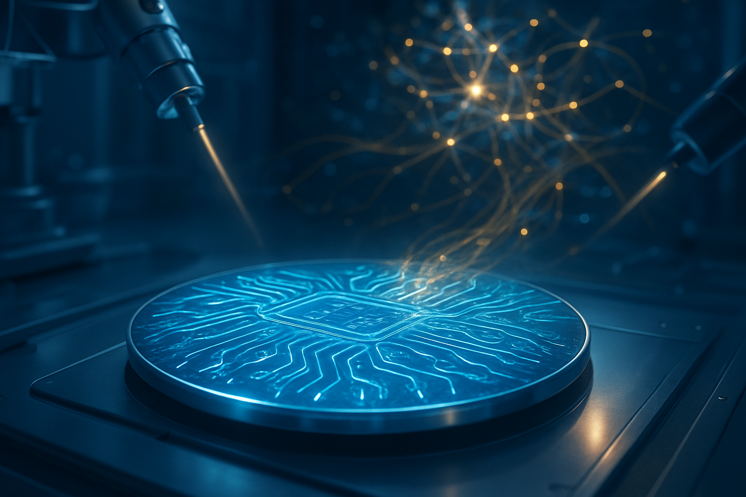
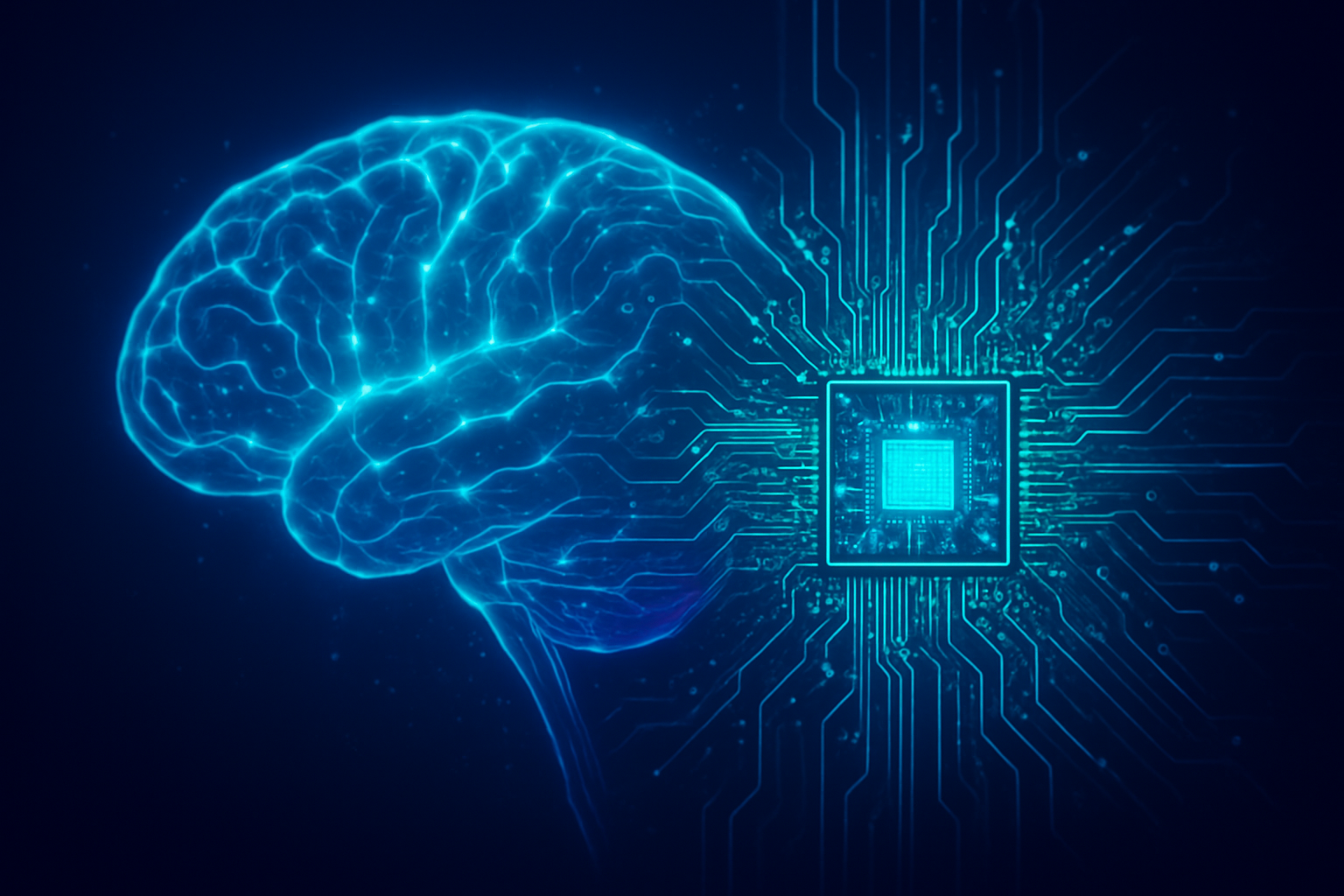
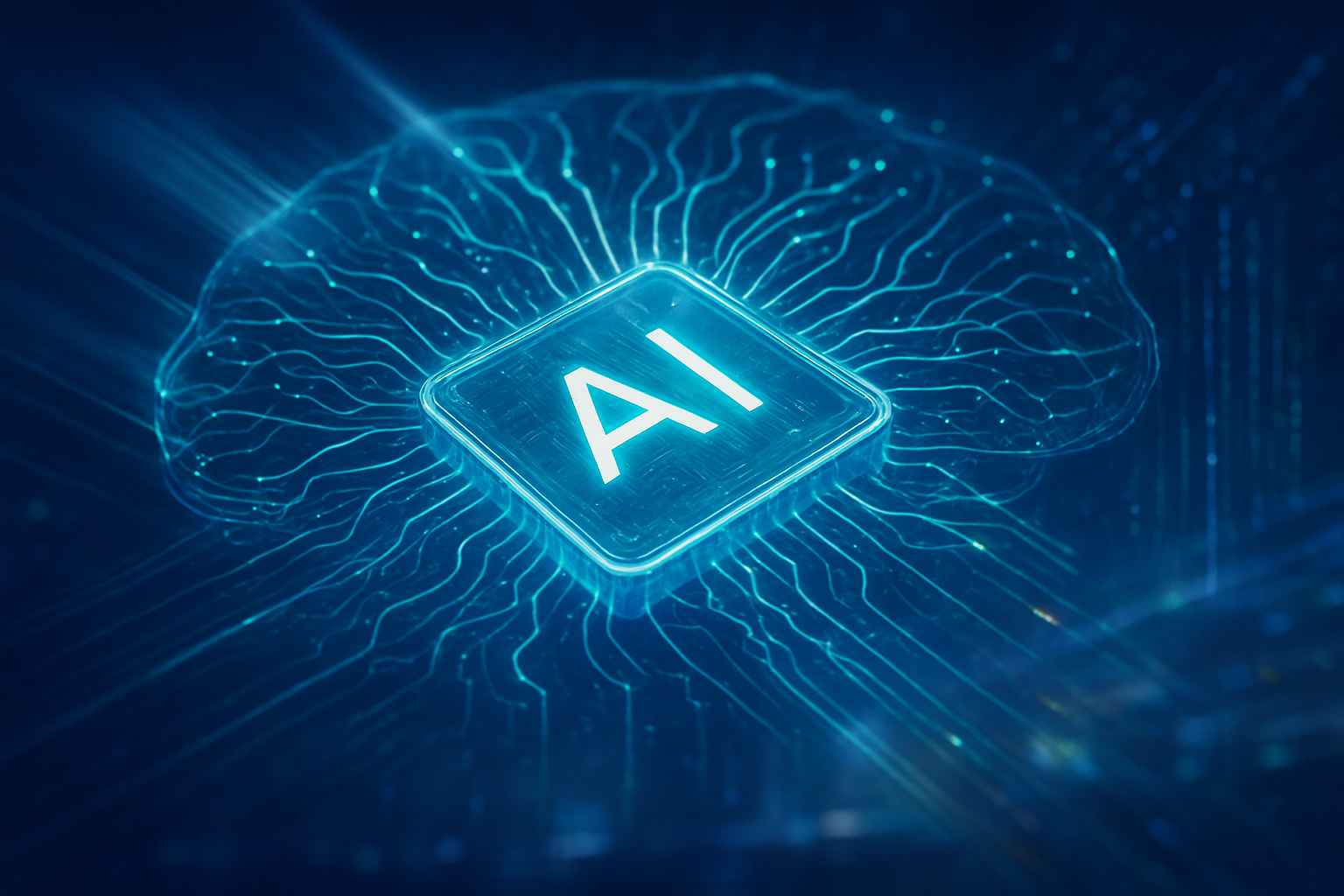
    Neuromorphic computing represents a radical departure from traditional computer architectures, mimicking the human brain's intricate structure and function to create more efficient and powerful processing systems. Unlike conventional Von Neumann machines that separate processing and memory, neuromorphic chips integrate these functions directly within "artificial neurons" and "synapses." This brain-like design leverages spiking neural networks (SNNs), where computations occur in an event-driven, parallel manner, consuming energy only when neurons "spike" in response to signals, much like biological brains. This fundamental shift allows neuromorphic systems to excel in adaptability, real-time learning, and the simultaneous processing of multiple tasks.

    The immediate significance of neuromorphic computing for advanced AI chips is transformative, addressing critical bottlenecks in current AI processing capabilities. Modern AI, particularly large language models and real-time sensory data processing, demands immense computational power and energy, often pushing traditional GPUs to their limits. Neuromorphic chips offer a compelling solution by delivering unparalleled energy efficiency, often consuming orders of magnitude less power for certain AI inference tasks. This efficiency, coupled with their inherent ability for real-time, low-latency decision-making, makes them ideal for crucial AI applications such as autonomous vehicles, robotics, cybersecurity, and advanced edge AI devices where continuous, intelligent processing with minimal power draw is essential. By fundamentally redesigning how AI hardware learns and processes information, neuromorphic computing is poised to accelerate AI development and enable a new generation of intelligent, responsive, and sustainable AI systems.

    The Architecture of Intelligence: Diving Deep into Neuromorphic and Traditional AI Chips

    Neuromorphic computing and advanced AI chips represent significant shifts in computational architecture, aiming to overcome the limitations of traditional von Neumann designs, particularly for artificial intelligence workloads. These innovations draw inspiration from the human brain's structure and function to deliver enhanced efficiency, adaptability, and processing capabilities.

    Neuromorphic computing, also known as neuromorphic engineering, is an approach to computing that mimics the way the human brain works, designing both hardware and software to simulate neural and synaptic structures and functions. This paradigm uses artificial neurons to perform computations, prioritizing robustness, adaptability, and learning by emulating the brain's distributed processing across small computing elements. Key technical principles include Spiking Neural Networks (SNNs) for event-driven, asynchronous processing, collocated memory and processing to eliminate the von Neumann bottleneck, massive parallelism, and exceptional energy efficiency, often consuming orders of magnitude less power. Many neuromorphic processors also support on-chip learning, allowing them to adapt in real-time.

    Leading the charge in neuromorphic hardware development are several key players. IBM (NYSE: IBM) has been a pioneer with its TrueNorth chip (released in 2015), featuring 1 million programmable spiking neurons and 256 million programmable synapses, consuming a mere 70 milliwatts. Its more recent "NorthPole" chip (2023), built on a 12nm process with 22 billion transistors, boasts 25 times more energy efficiency and is 22 times faster than NVIDIA's (NASDAQ: NVDA) V100 GPU for specific inference tasks. Intel (NASDAQ: INTC) has made significant strides with its Loihi research chips. Loihi 1 (2018) included 128 neuromorphic cores and up to 130,000 synthetic neurons. Loihi 2 (2021), fabricated on Intel's 4 process (7nm EUV), scaled up to 1 million neurons per chip and 120 million synapses, offering 10x faster spike processing. Intel's latest, Hala Point (2024), is a large-scale system with 1.15 billion neurons, demonstrating capabilities 50 times faster and 100 times more energy-efficient than conventional CPU/GPU systems for certain AI workloads. The University of Manchester's SpiNNaker project also contributes significantly with its highly parallel, event-driven architecture.

    In contrast, traditional AI chips, like Graphics Processing Units (GPUs), Tensor Processing Units (TPUs), and Application-Specific Integrated Circuits (ASICs), accelerate AI by performing complex mathematical computations and massively parallel processing. NVIDIA's (NASDAQ: NVDA) H100 Tensor Core GPU, based on the Hopper architecture, delivers up to 9x the performance of its predecessor for AI processing, featuring specialized Tensor Cores and a Transformer Engine. Its successor, the Blackwell architecture, aims for up to 25 times better energy efficiency for training trillion-parameter models, boasting over 208 billion transistors. Google's custom-developed TPUs (e.g., TPU v5) are ASICs specifically optimized for machine learning workloads, offering fast matrix multiplication and inference. Other ASICs like Graphcore's Colossus MK2 (IPU-M2000) also provide immense computing power. Neural Processing Units (NPUs) found in consumer devices, such as Apple's (NASDAQ: AAPL) M2 Ultra (16-core Neural Engine, 22 trillion operations per second) and Qualcomm's (NASDAQ: QCOM) Snapdragon platforms, focus on efficient, real-time on-device inference for tasks like image recognition and natural language processing.

    The fundamental difference lies in their architectural inspiration and operational paradigm. Traditional AI chips adhere to the von Neumann architecture, separating processing and memory, leading to the "von Neumann bottleneck." They use synchronous, clock-driven processing with continuous values, demanding substantial power. Neuromorphic chips, however, integrate memory and processing, employ asynchronous, event-driven spiking neural networks, and consume power only when neurons activate. This leads to drastically reduced power consumption and inherent support for real-time, continuous, and adaptive learning directly on the chip, making them more fault-tolerant and capable of responding to evolving stimuli without extensive retraining.

    Initial reactions from the AI research community and industry experts have been overwhelmingly positive, citing neuromorphic computing as a "breakthrough year" for its transition from academic pursuit to tangible commercial products. Experts highlight energy efficiency, real-time processing, adaptability, enhanced pattern recognition, and the ability to overcome the von Neumann bottleneck as primary advantages. Many view it as a growth accelerator for AI, potentially boosting high-performance computing and even paving the way for Artificial General Intelligence (AGI). However, challenges remain, including potential accuracy concerns when converting deep neural networks to SNNs, a limited and underdeveloped software ecosystem, scalability issues, high processing latency in some real-world applications, and the significant investment required for research and development. The complexity and need for interdisciplinary expertise also present hurdles, alongside the challenge of competing with entrenched incumbents like NVIDIA (NASDAQ: NVDA) in the cloud and data center markets.

    Shifting Sands: How Neuromorphic Computing Reshapes the AI Industry

    Neuromorphic computing is poised to significantly impact AI companies, tech giants, and startups by offering unparalleled energy efficiency, real-time processing, and adaptive learning capabilities. This paradigm shift, leveraging brain-inspired hardware and spiking neural networks, is creating a dynamic competitive landscape.

    AI companies focused purely on AI development stand to benefit immensely from neuromorphic computing's ability to handle complex AI tasks with significantly reduced power consumption and lower latency. This enables the deployment of more sophisticated AI models, especially at the edge, providing real-time, context-aware decision-making for autonomous systems and robotics. These companies can leverage the technology to develop advanced applications in predictive analytics, personalized user experiences, and optimized workflows, leading to reduced operational costs.

    Major technology companies are heavily invested, viewing neuromorphic computing as crucial for the future of AI. Intel (NASDAQ: INTC), with its Loihi research chips and the large-scale Hala Point system, aims to perform AI workloads significantly faster and with less energy than conventional CPU/GPU systems, targeting sustainable AI research. IBM (NYSE: IBM), through its TrueNorth and NorthPole chips, is advancing brain-inspired systems to process vast amounts of data with tablet-level power consumption. Qualcomm (NASDAQ: QCOM) has been working on its "Zeroth" platform (NPU) for mobile devices, focusing on embedded cognition and real-time learning. Other tech giants like Samsung (KRX: 005930), Sony (NYSE: SONY), AMD (NASDAQ: AMD), NXP Semiconductors (NASDAQ: NXPI), and Hewlett Packard Enterprise (NYSE: HPE) are also active, often integrating neuromorphic principles into their product lines to offer specialized hardware with significant performance-per-watt improvements.

    Numerous startups are also emerging as key innovators, often focusing on niche applications and ultra-low-power edge AI solutions. BrainChip (ASX: BRN) is a leader in commercializing neuromorphic technology with its Akida processor, designed for low-power edge AI in automotive, healthcare, and cybersecurity. GrAI Matter Labs focuses on ultra-low latency, low-power AI processors for edge applications, while SynSense (formerly aiCTX) specializes in ultra-low-power vision and sensor fusion. Other notable startups include Innatera, Prophesee, Aspirare Semi, Vivum Computing, Blumind, and Neurobus, each contributing to specialized areas within the neuromorphic ecosystem.

    Neuromorphic computing poses a significant potential disruption. While not replacing general-purpose computing entirely, these chips excel at specific AI workloads requiring real-time processing, low power, and continuous learning at the edge. This could reduce reliance on power-hungry CPUs and GPUs for these specialized tasks, particularly for inference. It could also revolutionize Edge AI and IoT, enabling a new generation of smart devices capable of complex local AI tasks without constant cloud connectivity, addressing privacy concerns and reducing bandwidth. The need for specialized software and algorithms, such as spiking neural networks (SNNs), will also disrupt existing AI software ecosystems, creating a demand for new development environments and expertise.

    The neuromorphic computing market is an emerging field with substantial growth potential, projected to reach USD 1,325.2 million by 2030, growing at a CAGR of 89.7% from 2024. Currently, it is best suited for challenges where its unique advantages are critical, such as pattern recognition, sensory processing, and continuous learning in dynamic environments. It offers a more sustainable path for AI development by drastically reducing power consumption, aligning with growing ESG standards. Initially, neuromorphic systems will likely complement traditional computing in hybrid architectures, offloading latency-critical AI workloads. The market is driven by significant investments from governments and major tech companies, though challenges remain regarding production costs, accessibility, and the scarcity of specialized programming expertise.

    Beyond the Bottleneck: Neuromorphic Computing's Broader Impact on AI and Society

    Neuromorphic computing represents a distinct paradigm within the broader AI landscape, differing fundamentally from deep learning, which is primarily a software algorithm running on conventional hardware like GPUs. While both are inspired by the brain, neuromorphic computing builds neurons directly into the hardware, often using spiking neural networks (SNNs) that communicate via electrical pulses, similar to biological neurons. This contrasts with deep neural networks (DNNs) that typically use continuous, more structured processing.

    The wider significance of neuromorphic computing stems primarily from its potential to overcome the limitations of conventional computing systems, particularly in terms of energy efficiency and real-time processing. By integrating processing and memory, mimicking the brain's highly parallel and event-driven nature, neuromorphic chips drastically reduce power consumption—potentially 1,000 times less for some functions—making them ideal for power-constrained applications. This fundamental design allows for low-latency, real-time computation and continuous learning from new data without constant retraining, crucial for handling unpredictable real-world scenarios. It effectively circumvents the "von Neumann bottleneck" and offers inherent robustness and fault tolerance.

    Neuromorphic computing is not necessarily a replacement for current AI, but rather a complementary technology that can enhance AI capabilities, especially where energy efficiency and real-time, on-device learning are critical. It aligns perfectly with several key AI trends: the rise of Edge AI, where processing occurs close to the data source; the increasing demand for Sustainable AI due to the massive energy footprint of large-scale models; and the quest for solutions beyond Moore's Law as traditional computing approaches face physical limitations. Researchers are actively exploring hybrid systems that combine neuromorphic and conventional computing elements to leverage the strengths of both.

    The impacts of neuromorphic computing are far-reaching. In robotics, it enables more adaptive and intelligent machines that learn from their environment. For autonomous vehicles, it provides real-time sensory data processing for split-second decision-making. In healthcare, applications range from enhanced diagnostics and real-time neuroprosthetics to seizure prediction systems. It will empower IoT and smart cities with local data analysis, reducing latency and bandwidth. In cybersecurity, neuromorphic chips could continuously learn from network traffic to detect evolving threats. Other sectors like manufacturing, energy, finance, and telecommunications also stand to benefit from optimized processes and enhanced analytics. Ultimately, the potential for cost-saving in AI training and deployment could democratize access to advanced computing.

    Despite its promise, neuromorphic computing faces several challenges and potential concerns. The high cost of development and manufacturing, coupled with limited commercial adoption, restricts accessibility. There is a significant need for a new, underdeveloped software ecosystem tailored for asynchronous, event-driven systems, as well as a lack of standardized benchmarks. Scalability and latency issues, along with potential accuracy concerns when converting deep neural networks to spiking ones, remain hurdles. The interdisciplinary complexity of the field and the learning curve for developers also present challenges. Ethically, as machines become more brain-like and capable of autonomous decision-making, profound questions arise concerning accountability, privacy, and the potential for artificial consciousness, demanding careful regulation and oversight, particularly in areas like autonomous weapons and brain-machine interfaces.

    Neuromorphic computing can be seen as a significant evolutionary step in AI history, distinguishing itself from previous milestones. While early AI (Perceptrons, Expert Systems) laid foundational work and deep learning (DNNs, Backpropagation) achieved immense success through software simulations on traditional hardware, neuromorphic computing represents a fundamental re-imagining of the hardware itself. It aims to replicate the physical and functional aspects of biological neurons and synapses directly in silicon, moving beyond the von Neumann architecture's memory wall. This shift towards a more "brain-like" way of learning and adapting, with the potential to handle uncertainty and learn through observation, marks a paradigm shift from previous milestones where semiconductors merely enabled AI; now, AI is co-created with its specialized hardware.

    The Road Ahead: Navigating the Future of Neuromorphic AI

    Neuromorphic computing, with its brain-inspired architecture, is poised to revolutionize artificial intelligence and various other fields. This nascent field is expected to see substantial developments in both the near and long term, impacting a wide range of applications while also grappling with significant challenges.

    In the near term (within 1-5 years, extending to 2030), neuromorphic computing is expected to see widespread adoption in Edge AI and Internet of Things (IoT) devices. These chips will power smart home devices, drones, robots, and various sensors, enabling local, real-time data processing without constant reliance on cloud servers. This will lead to enhanced AI capabilities, allowing devices to handle the unpredictability of the real world by efficiently detecting events, recognizing patterns, and performing training with smaller datasets. Energy efficiency will be a critical driver, particularly in power-sensitive scenarios, with experts predicting the integration of neuromorphic chips into smartphones by 2025. Advancements in materials science, focusing on memristors and other non-volatile memory devices, are crucial for more brain-like behavior and efficient on-chip learning. The development of hybrid architectures combining neuromorphic chips with conventional CPUs and GPUs is also anticipated, leveraging the strengths of each for diverse computational needs.

    Looking further ahead, the long-term vision for neuromorphic computing centers on achieving truly cognitive AI and Artificial General Intelligence (AGI). Neuromorphic systems are considered one of the most biologically plausible paths toward AGI, promising new paradigms of AI that are not only more efficient but also more explainable, robust, and generalizable. Researchers aim to build neuromorphic computers with neuron counts comparable to the human cerebral cortex, capable of operating orders of magnitude faster than biological brains while consuming significantly less power. This approach is expected to revolutionize AI by enabling algorithms to run predominantly at the edge and address the anticipated end of Moore's Law.

    Neuromorphic computing's brain-inspired architecture offers a wide array of potential applications across numerous sectors. These include:

    • Edge AI and IoT: Enabling intelligent processing on devices with limited power.
    • Image and Video Recognition: Enhancing capabilities in surveillance, self-driving cars, and medical imaging.
    • Robotics: Creating more adaptive and intelligent robots that learn from their environment.
    • Healthcare and Medical Applications: Facilitating real-time disease diagnosis, personalized drug discovery, and intelligent prosthetics.
    • Autonomous Vehicles: Providing real-time decision-making capabilities and efficient sensor data processing.
    • Natural Language Processing (NLP) and Speech Processing: Improving the understanding and generation capacities of NLP models.
    • Fraud Detection: Identifying unusual patterns in transaction data more efficiently.
    • Neuroscience Research: Offering a powerful platform to simulate and study brain functions.
    • Optimization and Resource Management: Leveraging parallel processing for complex systems like supply chains and energy grids.
    • Cybersecurity: Detecting evolving and novel patterns of threats in real-time.

    Despite its promising future, neuromorphic computing faces several significant hurdles. A major challenge is the lack of a model hierarchy and an underdeveloped software ecosystem, making scaling and universality difficult. Developing algorithms that accurately mimic intricate neural processes is complex, and current biologically inspired algorithms may not yet match the accuracy of deep learning's backpropagation. The field also requires deep interdisciplinary expertise, making talent acquisition challenging. Scalability and training issues, particularly in distributing vast amounts of memory among numerous processors and the need for individual training, remain significant. Current neuromorphic processors, like Intel's (NASDAQ: INTC) Loihi, still struggle with high processing latency in certain real-world applications. Limited commercial adoption and a lack of standardized benchmarks further hinder widespread integration.

    Experts widely predict that neuromorphic computing will profoundly impact the future of AI, revolutionizing AI computing by enabling algorithms to run efficiently at the edge due to their smaller size and low power consumption, thereby reducing reliance on energy-intensive cloud computing. This paradigm shift is also seen as a crucial solution to address the anticipated end of Moore's Law. The market for neuromorphic computing is projected for substantial growth, with some estimates forecasting it to reach USD 54.05 billion by 2035. The future of AI is envisioned as a "marriage of physics and neuroscience," with AI itself playing a critical role in accelerating semiconductor innovation. The emergence of hybrid architectures, combining traditional CPU/GPU cores with neuromorphic processors, is a likely near-term development, leveraging the strengths of each technology. The ultimate long-term prediction includes the potential for neuromorphic computing to unlock the path toward Artificial General Intelligence by fostering more efficient learning, real-time adaptation, and robust information processing capabilities.

    The Dawn of Brain-Inspired AI: A Comprehensive Look at Neuromorphic Computing's Ascendancy

    Neuromorphic computing represents a groundbreaking paradigm shift in artificial intelligence, moving beyond conventional computing to mimic the unparalleled efficiency and adaptability of the human brain. This technology, characterized by its integration of processing and memory within artificial neurons and synapses, promises to unlock a new era of AI capabilities, particularly for energy-constrained and real-time applications.

    The key takeaways from this exploration highlight neuromorphic computing's core strengths: its extreme energy efficiency, often reducing power consumption by orders of magnitude compared to traditional AI chips; its capacity for real-time processing and continuous adaptability through spiking neural networks (SNNs); and its ability to overcome the von Neumann bottleneck by co-locating memory and computation. Companies like IBM (NYSE: IBM) and Intel (NASDAQ: INTC) are leading the charge in hardware development, with chips like NorthPole and Hala Point demonstrating significant performance and efficiency gains. These advancements are critical for driving AI forward in areas like autonomous vehicles, robotics, edge AI, and cybersecurity.

    In the annals of AI history, neuromorphic computing is not merely an incremental improvement but a fundamental re-imagining of the hardware itself. While earlier AI milestones focused on algorithmic breakthroughs and software running on traditional architectures, neuromorphic computing directly embeds brain-like functionality into silicon. This approach is seen as a "growth accelerator for AI" and a potential pathway to Artificial General Intelligence, addressing the escalating energy demands of modern AI and offering a sustainable solution beyond the limitations of Moore's Law. Its significance lies in enabling AI systems to learn, adapt, and operate with an efficiency and robustness closer to biological intelligence.

    The long-term impact of neuromorphic computing is expected to be profound, transforming human interaction with intelligent machines and integrating brain-like capabilities into a vast array of devices. It promises a future where AI systems are not only more powerful but also significantly more energy-efficient, potentially matching the power consumption of the human brain. This will enable more robust AI models capable of operating effectively in dynamic, unpredictable real-world environments. The projected substantial growth of the neuromorphic computing market underscores its potential to become a cornerstone of future AI development, driving innovation in areas from advanced robotics to personalized healthcare.

    In the coming weeks and months, several critical areas warrant close attention. Watch for continued advancements in chip design and materials, particularly the integration of novel memristive devices and hybrid architectures that further mimic biological synapses. Progress in software and algorithm development for neuromorphic systems is crucial, as is the push towards scaling and standardization to ensure broader adoption and interoperability. Keep an eye on increased collaborations and funding initiatives between academia, industry, and government, which will accelerate research and development. Finally, observe the emergence of new applications and proof points in fields like autonomous drones, real-time medical diagnostics, and enhanced cybersecurity, which will demonstrate the practical viability and growing impact of this transformative technology. Experiments combining neuromorphic computing with quantum computing and "brain-on-chip" innovations could also open entirely new frontiers.


    This content is intended for informational purposes only and represents analysis of current AI developments.

    TokenRing AI delivers enterprise-grade solutions for multi-agent AI workflow orchestration, AI-powered development tools, and seamless remote collaboration platforms.
    For more information, visit https://www.tokenring.ai/.

  • AI Chips Unleashed: The 2025 Revolution in Brain-Inspired Designs, Optical Speed, and Modular Manufacturing

    AI Chips Unleashed: The 2025 Revolution in Brain-Inspired Designs, Optical Speed, and Modular Manufacturing

    November 2025 marks an unprecedented surge in AI chip innovation, characterized by the commercialization of brain-like computing, a leap into light-speed processing, and a manufacturing paradigm shift towards modularity and AI-driven efficiency. These breakthroughs are immediately reshaping the technological landscape, driving sustainable, powerful AI from the cloud to the farthest edge of the network.

    The artificial intelligence hardware sector is currently undergoing a profound transformation, with significant advancements in both chip design and manufacturing processes directly addressing the escalating demands for performance, energy efficiency, and scalability. The immediate significance of these developments lies in their capacity to accelerate AI deployment across industries, drastically reduce its environmental footprint, and enable a new generation of intelligent applications that were previously out of reach due to computational or power constraints.

    Technical Deep Dive: The Engines of Tomorrow's AI

    The core of this revolution lies in several distinct yet interconnected technical advancements. Neuromorphic computing, which mimics the human brain's neural architecture, is finally moving beyond theoretical research into practical, commercial applications. Chips like Intel's (NASDAQ: INTC) Hala Point system, BrainChip's (ASX: BRN) Akida Pulsar, and Innatera's Spiking Neural Processor (SNP), have seen significant advancements or commercial launches in 2025. These systems are inherently energy-efficient, offering low-latency solutions ideal for edge AI, robotics, and the Internet of Things (IoT). For instance, Akida Pulsar boasts up to 500 times lower energy consumption and 100 times latency reduction compared to conventional AI cores for real-time, event-driven processing at the edge. Furthermore, USC researchers have demonstrated artificial neurons that replicate biological function with significantly reduced chip size and energy consumption, promising to advance artificial general intelligence. This paradigm shift directly addresses the critical need for sustainable AI by drastically cutting power usage in resource-constrained environments.

    Another major bottleneck in traditional computing architectures, the "memory wall," is being shattered by in-memory computing (IMC) and processing-in-memory (PIM) chips. These innovative designs perform computations directly within memory, dramatically reducing the movement of data between the processor and memory. This reduction in data transfer, in turn, slashes power consumption and significantly boosts processing speed. Companies like Qualcomm (NASDAQ: QCOM) are integrating near-memory computing into new solutions such as the AI250, providing a generational leap in effective memory bandwidth and efficiency specifically for AI inference workloads. This technology is crucial for managing the massive data processing demands of complex AI algorithms, enabling faster and more efficient training and inference for burgeoning generative AI models and large language models (LLMs).

    Perhaps one of the most futuristic developments is the emergence of optical computing. Scientists at Tsinghua University have achieved a significant milestone by developing a light-powered AI chip, OFE², capable of handling data at an unprecedented 12.5 GHz. This optical computing breakthrough completes complex pattern-recognition tasks by directing light beams through on-chip structures, consuming significantly less energy than traditional electronic devices. This innovation offers a potent solution to the growing energy demands of AI, potentially freeing AI from being a major contributor to global energy shortages. It promises a new generation of real-time, ultra-low-energy AI, crucial for sustainable and widespread deployment across various sectors.

    Finally, as traditional transistor scaling (often referred to as Moore's Law) faces physical limits, advanced packaging technologies and chiplet architectures have become paramount. Technologies like 2.5D and 3D stacking (e.g., CoWoS, 3DIC), Fan-Out Panel-Level Packaging (FO-PLP), and hybrid bonding are crucial for boosting performance, increasing integration density, improving signal integrity, and enhancing thermal management for AI chips. Complementing this, chiplet technology, which involves modularizing chip functions into discrete components, is gaining significant traction, with the Universal Chiplet Interconnect Express (UCIe) standard expanding its adoption. These innovations are the new frontier for hardware optimization, offering flexibility, cost-effectiveness, and faster development cycles. They also mitigate supply chain risks by allowing manufacturers to source different parts from multiple suppliers. The market for advanced packaging is projected to grow eightfold by 2033, underscoring its immediate importance for the widespread adoption of AI chips into consumer devices and automotive applications.

    Competitive Landscape: Winners and Disruptors

    These advancements are creating clear winners and potential disruptors within the AI industry. Chip designers and manufacturers at the forefront of these innovations stand to benefit immensely. Intel, with its neuromorphic Hala Point system, and BrainChip, with its Akida Pulsar, are well-positioned in the energy-efficient edge AI market. Qualcomm's integration of near-memory computing in its AI250 strengthens its leadership in mobile and edge AI processing. NVIDIA (NASDAQ: NVDA), while not explicitly mentioned for neuromorphic or optical chips, continues to dominate the high-performance computing space for AI training and is a key enabler for AI-driven manufacturing.

    The competitive implications are significant. Major AI labs and tech companies reliant on traditional architectures will face pressure to adapt or risk falling behind in performance and energy efficiency. Companies that can rapidly integrate these new chip designs into their products and services will gain a substantial strategic advantage. For instance, the ability to deploy AI models with significantly lower power consumption opens up new markets in battery-powered devices, remote sensing, and pervasive AI. The modularity offered by chiplets could also democratize chip design to some extent, allowing smaller players to combine specialized chiplets from various vendors to create custom, high-performance AI solutions, potentially disrupting the vertically integrated chip design model.

    Furthermore, AI's role in optimizing its own creation is a game-changer. AI-driven Electronic Design Automation (EDA) tools are dramatically accelerating chip design timelines—for example, reducing a 5nm chip's optimization cycle from six months to just six weeks. This means faster time-to-market for new AI chips, improved design quality, and more efficient, higher-yield manufacturing processes. Samsung (KRX: 005930), for instance, is establishing an "AI Megafactory" powered by 50,000 NVIDIA GPUs to revolutionize its chip production, integrating AI throughout its entire manufacturing flow. Similarly, SK Group is building an "AI factory" in South Korea with NVIDIA, focusing on next-generation memory and autonomous fab digital twins to optimize efficiency. These efforts are critical for meeting the skyrocketing demand for AI-optimized semiconductors and bolstering supply chain resilience amidst geopolitical shifts.

    Broader Significance: Shaping the AI Future

    These innovations fit perfectly into the broader AI landscape, addressing critical trends such as the insatiable demand for computational power for increasingly complex models (like LLMs), the push for sustainable and energy-efficient AI, and the proliferation of AI at the edge. The move towards neuromorphic and optical computing represents a fundamental shift away from the Von Neumann architecture, which has dominated computing for decades, towards more biologically inspired or physically optimized processing methods. This transition is not merely an incremental improvement but a foundational change that could unlock new capabilities in AI.

    The impacts are far-reaching. On one hand, these advancements promise more powerful, ubiquitous, and efficient AI, enabling breakthroughs in areas like personalized medicine, autonomous systems, and advanced scientific research. On the other hand, potential concerns, while mitigated by the focus on energy efficiency, still exist regarding the ethical implications of more powerful AI and the increasing complexity of hardware development. However, the current trajectory is largely positive, aiming to make AI more accessible and environmentally responsible.

    Comparing this to previous AI milestones, such as the rise of GPUs for deep learning or the development of specialized AI accelerators like Google's TPUs, these current advancements represent a diversification and deepening of the hardware foundation. While earlier milestones focused on brute-force parallelization, today's innovations are about architectural efficiency, novel physics, and self-optimization through AI, pushing beyond the limits of traditional silicon. This multi-pronged approach suggests a more robust and sustainable path for AI's continued growth.

    The Road Ahead: Future Developments and Challenges

    Looking to the near-term, we can expect to see further integration of these technologies. Hybrid chips combining neuromorphic, in-memory, and conventional processing units will likely become more common, optimizing specific workloads for maximum efficiency. The UCIe standard for chiplets will continue to gain traction, leading to a more modular and customizable AI hardware ecosystem. In the long-term, the full potential of optical computing, particularly in areas requiring ultra-high bandwidth and low latency, could revolutionize data centers and telecommunications infrastructure, creating entirely new classes of AI applications.

    Potential applications on the horizon include highly sophisticated, real-time edge AI for autonomous vehicles that can process vast sensor data with minimal latency and power, advanced robotics capable of learning and adapting in complex environments, and medical devices that can perform on-device diagnostics with unprecedented accuracy and speed. Generative AI and LLMs will also see significant performance boosts, enabling more complex and nuanced interactions, and potentially leading to more human-like AI capabilities.

    However, challenges remain. Scaling these nascent technologies to mass production while maintaining cost-effectiveness is a significant hurdle. The development of robust software ecosystems and programming models that can fully leverage the unique architectures of neuromorphic and optical chips will be crucial. Furthermore, ensuring interoperability between diverse chiplet designs and maintaining supply chain stability amidst global economic fluctuations will require continued innovation and international collaboration. Experts predict a continued convergence of hardware and software co-design, with AI playing an ever-increasing role in optimizing its own underlying infrastructure.

    A New Era for AI Hardware

    In summary, the latest innovations in AI chip design and manufacturing—encompassing neuromorphic computing, in-memory processing, optical chips, advanced packaging, and AI-driven manufacturing—represent a pivotal moment in the history of artificial intelligence. These breakthroughs are not merely incremental improvements but fundamental shifts that promise to make AI more powerful, energy-efficient, and ubiquitous than ever before.

    The significance of these developments cannot be overstated. They are addressing the core challenges of AI scalability and sustainability, paving the way for a future where AI is seamlessly integrated into every facet of our lives, from smart cities to personalized health. As we move forward, the interplay between novel chip architectures, advanced manufacturing techniques, and AI's self-optimizing capabilities will be critical to watch. The coming weeks and months will undoubtedly bring further announcements and demonstrations as companies race to capitalize on these transformative technologies, solidifying this period as a new era for AI hardware.


    This content is intended for informational purposes only and represents analysis of current AI developments.

    TokenRing AI delivers enterprise-grade solutions for multi-agent AI workflow orchestration, AI-powered development tools, and seamless remote collaboration platforms.
    For more information, visit https://www.tokenring.ai/.