Tag: Hardware

  • The Silicon Shift: Google’s TPU v7 Dethrones the GPU Hegemony in Historic Hardware Milestone

    The Silicon Shift: Google’s TPU v7 Dethrones the GPU Hegemony in Historic Hardware Milestone

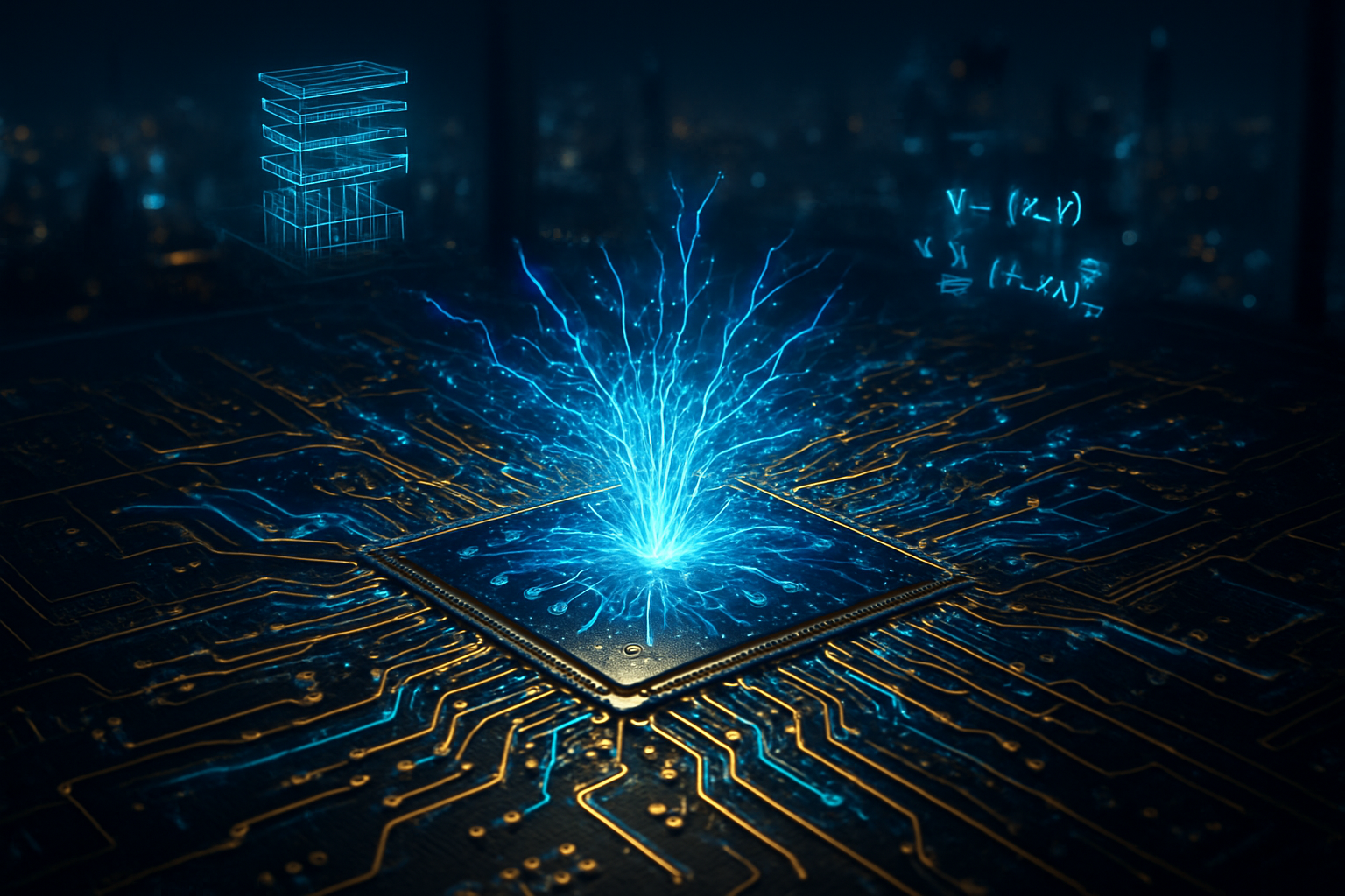
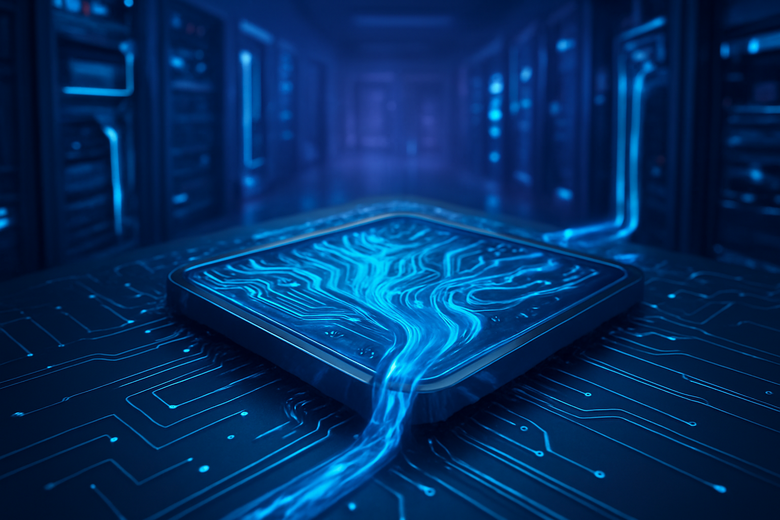
    The hierarchy of artificial intelligence hardware underwent a seismic shift in January 2026, as Google, a subsidiary of Alphabet Inc. (NASDAQ:GOOGL), officially confirmed that its custom-designed Tensor Processing Units (TPUs) have outshipped general-purpose GPUs in volume for the first time. This landmark achievement marks the end of a decade-long era where general-purpose graphics chips were the undisputed kings of AI training and inference. The surge in production is spearheaded by the TPU v7, codenamed "Ironwood," which has entered mass production to meet the insatiable demand of the generative AI boom.

    The news comes as a direct result of Google’s strategic pivot toward vertical integration, culminating in a massive partnership with AI lab Anthropic. The agreement involves the deployment of over 1 million TPU units throughout 2026, a move that provides Anthropic with over 1 gigawatt of dedicated compute capacity. This unprecedented scale of custom silicon deployment signals a transition where hyperscale cloud providers are no longer just customers of hardware giants, but are now the primary architects of the silicon powering the next generation of intelligence.

    Technical Deep-Dive: The Ironwood Architecture

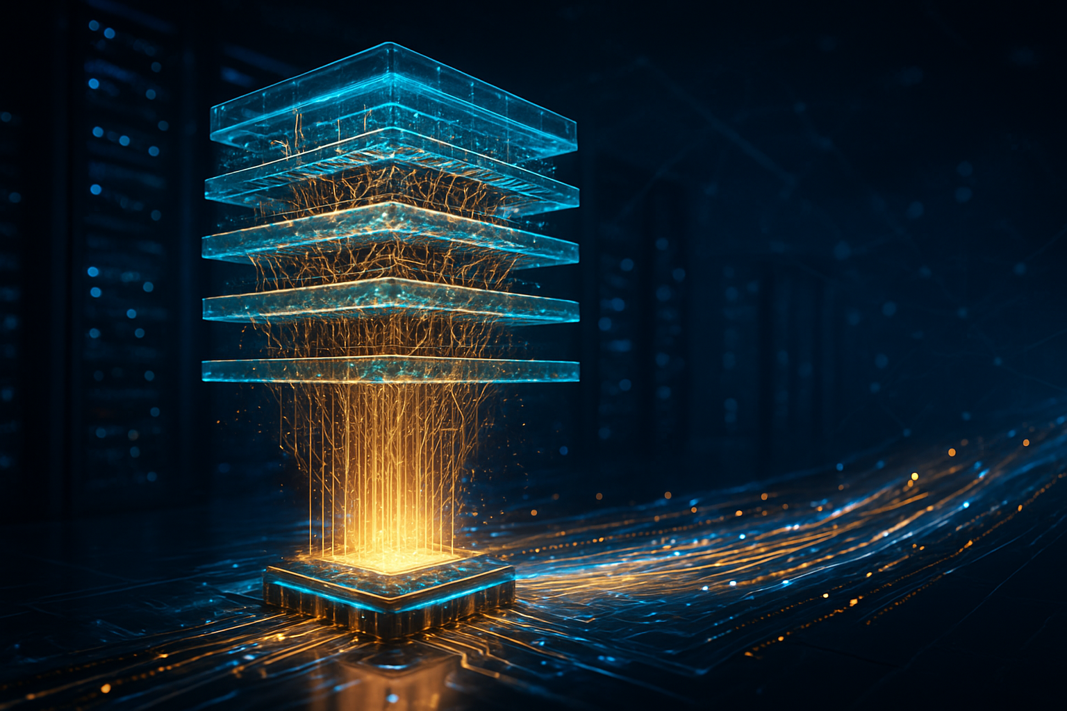
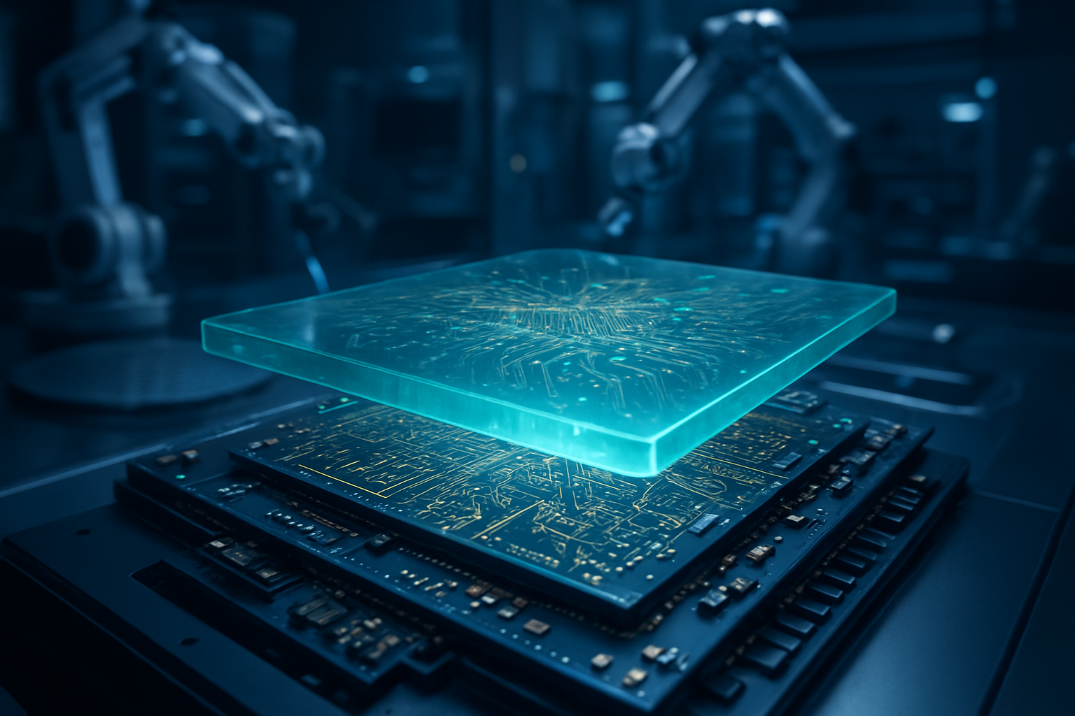
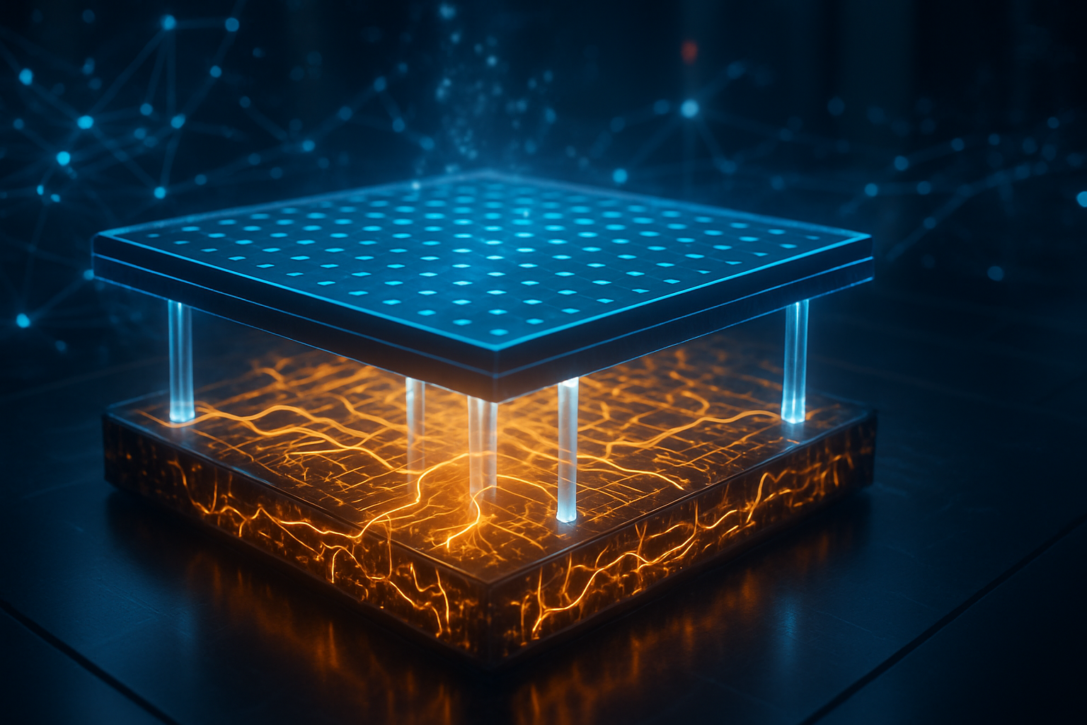
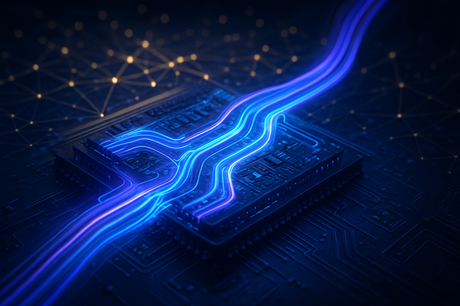
    The TPU v7 represents a radical departure from traditional chip design, utilizing a cutting-edge dual-chiplet architecture manufactured on a 3-nanometer process node by TSMC (NYSE:TSM). By moving away from monolithic dies, Google has managed to overcome the physical limits of "reticle size," allowing each TPU v7 to house two self-contained chiplets connected via a high-speed die-to-die (D2D) interface. Each chip boasts two TensorCores for massive matrix multiplication and four SparseCores, which are specifically optimized for the embedding-heavy workloads that drive modern recommendation engines and agentic AI models.

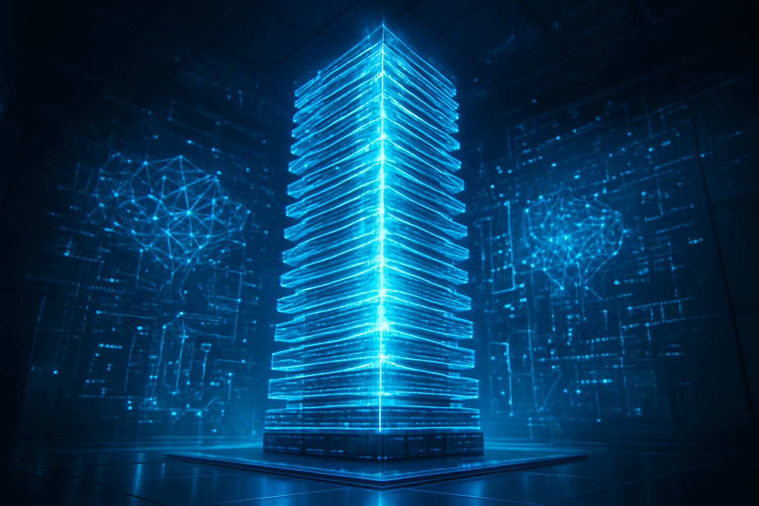
    Technically, the specifications of the Ironwood architecture are staggering. Each chip is equipped with 192 GB of HBM3e memory, delivering an unprecedented 7.37 TB/s of bandwidth. In terms of raw power, a single TPU v7 delivers 4.6 PFLOPS of FP8 compute. However, the true innovation lies in the networking; Google’s proprietary Optical Circuit Switching (OCS) allows for the interconnectivity of up to 9,216 chips in a single pod, creating a unified supercomputer capable of 42.5 FP8 ExaFLOPS. This optical interconnect system significantly reduces power consumption and latency by eliminating the need for traditional packet-switched electronic networking.

    This approach differs sharply from the general-purpose nature of the Blackwell and Rubin architectures from Nvidia (NASDAQ:NVDA). While Nvidia's chips are designed to be "Swiss Army knives" for any parallel computing task, the TPU v7 is a "scalpel," surgically precision-tuned for the transformer architectures and "thought signatures" required by advanced reasoning models. Initial reactions from the AI research community have been overwhelmingly positive, particularly following the release of the "vLLM TPU Plugin," which finally allows researchers to run standard PyTorch code on TPUs without the complex code rewrites previously required for Google’s JAX framework.

    Industry Impact and the End of the GPU Monopoly

    The implications for the competitive landscape of the tech industry are profound. Google’s ability to outship traditional GPUs effectively insulates the company—and its key partners like Anthropic—from the supply chain bottlenecks and high margins traditionally commanded by Nvidia. By controlling the entire stack from the silicon to the software, Google reported a 4.7-fold improvement in performance-per-dollar for inference workloads compared to equivalent H100 deployments. This cost advantage allows Google Cloud to offer "Agentic" compute at prices that startups reliant on third-party GPUs may find difficult to match.

    For Nvidia, the rise of the TPU v7 represents the most significant challenge to its dominance in the data center. While Nvidia recently unveiled its Rubin platform at CES 2026 to regain the performance lead, the "volume victory" of TPUs suggests that the market is bifurcating. High-end, versatile research may still favor GPUs, but the massive, standardized "factory-scale" inference that powers consumer-facing AI is increasingly moving toward custom ASICs. Other players like Advanced Micro Devices (NASDAQ:AMD) are also feeling the pressure, as the rising costs of HBM memory have forced price hikes on their Instinct accelerators, making the vertically integrated model of Google look even more attractive to enterprise customers.

    The partnership with Anthropic is particularly strategic. By securing 1 million TPU units, Anthropic has decoupled its future from the "GPU hunger games," ensuring it has the stable, predictable compute needed to train Claude 4 and Claude 4.5 Opus. This hybrid ownership model—where Anthropic owns roughly 400,000 units outright and rents the rest—could become a blueprint for how major AI labs interact with cloud providers moving forward, potentially disrupting the traditional "as-a-service" rental model in favor of long-term hardware residency.

    Broader Significance: The Era of Sovereign AI

    Looking at the broader AI landscape, the TPU v7 milestone reflects a trend toward "Sovereign Compute" and specialized hardware. As AI models move from simple chatbots to "Agentic AI"—systems that can perform multi-step reasoning and interact with software tools—the demand for chips that can handle "sparse" data and complex branching logic has skyrocketed. The TPU v7's SparseCores are a direct answer to this need, allowing for more efficient execution of models that don't need to activate every single parameter for every single request.

    This shift also brings potential concerns regarding the centralization of AI power. With only a handful of companies capable of designing 3nm custom silicon and operating OCS-enabled data centers, the barrier to entry for new hyperscale competitors has never been higher. Comparisons are being drawn to the early days of the mainframe or the transition to mobile SoC (System on a Chip) designs, where vertical integration became the only way to achieve peak efficiency. The environmental impact is also a major talking point; while the TPU v7 is twice as efficient per watt as its predecessor, the sheer scale of the 1-gigawatt Anthropic deployment underscores the massive energy requirements of the AI age.

    Historically, this event is being viewed as the "Hardware Decoupling." Much like how the software industry eventually moved from general-purpose CPUs to specialized accelerators for graphics and networking, the AI industry is now moving away from the "GPU-first" mindset. This transition validates the long-term vision Google began over a decade ago with the first TPU, proving that in the long run, custom-tailored silicon will almost always outperform a general-purpose alternative for a specific, high-volume task.

    Future Outlook: Scaling to the Zettascale

    In the near term, the industry is watching for the first results of models trained entirely on the 1-million-unit TPU cluster. Gemini 3.0, which is expected to launch later this year, will likely be the first test of whether this massive compute scale can eliminate the "reasoning drift" that has plagued earlier large language models. Experts predict that the success of the TPU v7 will trigger a "silicon arms race" among other cloud providers, with Amazon (NASDAQ:AMZN) and Meta (NASDAQ:META) likely to accelerate their own internal chip programs, Trainium and MTIA respectively, to catch up to Google’s volume.

    Future applications on the horizon include "Edge TPUs" derived from the v7 architecture, which could bring high-speed local inference to mobile devices and robotics. However, challenges remain—specifically the ongoing scarcity of HBM3e memory and the geopolitical complexities of 3nm fabrication. Analysts predict that if Google can maintain its production lead, it could become the primary provider of "AI Utility" compute, effectively turning AI processing into a standardized, high-efficiency commodity rather than a scarce luxury.

    A New Chapter in AI Hardware

    The January 2026 milestone of Google TPUs outshipping GPUs is more than just a statistical anomaly; it is a declaration of the new world order in AI infrastructure. By combining the technical prowess of the TPU v7 with the massive deployment scale of the Anthropic partnership, Alphabet has demonstrated that the future of AI belongs to those who own the silicon. The transition from general-purpose to purpose-built hardware is now complete, and the efficiencies gained from this shift will likely drive the next decade of AI innovation.

    As we look ahead, the key takeaways are clear: vertical integration is the ultimate competitive advantage, and "performance-per-dollar" has replaced "peak TFLOPS" as the metric that matters most to the enterprise. In the coming weeks, the industry will be watching for the response from Nvidia’s Rubin platform and the first performance benchmarks of the Claude 4 models. For now, the "Ironwood" era has begun, and the AI hardware market will never be the same.


    This content is intended for informational purposes only and represents analysis of current AI developments.

    TokenRing AI delivers enterprise-grade solutions for multi-agent AI workflow orchestration, AI-powered development tools, and seamless remote collaboration platforms.
    For more information, visit https://www.tokenring.ai/.

  • The Great Memory Wall Falls: SK Hynix Shatters Records with 16-Layer HBM4 at CES 2026

    The Great Memory Wall Falls: SK Hynix Shatters Records with 16-Layer HBM4 at CES 2026

    The artificial intelligence arms race has entered a transformative new phase following the conclusion of CES 2026, where the "memory wall"—the long-standing bottleneck in AI processing—was decisively breached. SK Hynix (KRX: 000660) took center stage to demonstrate its 16-layer High Bandwidth Memory 4 (HBM4) package, a technological marvel designed specifically to power NVIDIA’s (NASDAQ: NVDA) upcoming Rubin GPU architecture. This announcement marks the official start of the "HBM4 Supercycle," a structural shift in the semiconductor industry where memory is no longer a peripheral component but the primary driver of AI scaling.

    The immediate significance of this development cannot be overstated. As large language models (LLMs) and multi-modal AI systems grow in complexity, the speed at which data moves between the processor and memory has become more critical than the raw compute power of the chip itself. By delivering an unprecedented 2TB/s of bandwidth, SK Hynix has provided the necessary "fuel" for the next generation of generative AI, effectively enabling the training of models ten times larger than GPT-5 with significantly lower energy overhead.

    Doubling the Pipe: The Technical Architecture of HBM4

    The demonstration at CES 2026 showcased a fundamental departure from the HBM standards of the last decade. The most jarring technical specification is the transition to a 2048-bit interface, doubling the 1024-bit width that has been the industry standard since the original HBM. This "wider pipe" allows for massive data throughput without the need for extreme clock speeds, which helps keep the thermal profile of AI data centers manageable. Each 16-layer stack now achieves a bandwidth of 2TB/s, nearly 2.5 times the performance of the current HBM3e standard used in Blackwell-class systems.

    To achieve this 16-layer density, SK Hynix utilized its proprietary Advanced MR-MUF (Mass Reflow Molded Underfill) technology. The process involves thinning DRAM wafers to approximately 30μm—about a third the thickness of a human hair—to fit 16 layers within the JEDEC-standard 775μm height limit. This provides a staggering 48GB of capacity per stack. When integrated into NVIDIA’s Rubin platform, which utilizes eight such stacks, a single GPU will have access to 384GB of high-speed memory and an aggregate bandwidth exceeding 22TB/s.

    Initial reactions from the AI research community have been electric. Dr. Aris Xanthos, a senior hardware analyst, noted that "the shift to a 2048-bit interface is the single most important hardware milestone of 2026." Unlike previous generations, where memory was a "passive" storage bin, HBM4 introduces a "logic die" manufactured on advanced nodes. Through a strategic partnership with TSMC (NYSE: TSM), SK Hynix is using TSMC’s 12nm and 5nm logic processes for the base die. This allows for the integration of custom control logic directly into the memory stack, essentially turning the HBM into an active co-processor that can pre-process data before it even reaches the GPU.

    Strategic Alliances and the Death of Commodity Memory

    This development has profound implications for the competitive landscape of Silicon Valley. The "Foundry-Memory Alliance" between SK Hynix and TSMC has created a formidable moat that challenges the traditional business models of integrated giants like Samsung Electronics (KRX: 005930). By outsourcing the logic die to TSMC, SK Hynix has ensured that its memory is perfectly tuned for NVIDIA’s CoWoS-L (Chip on Wafer on Substrate) packaging, which is the backbone of the Vera Rubin systems. This "triad" of NVIDIA, TSMC, and SK Hynix currently dominates the high-end AI hardware market, leaving competitors scrambling to catch up.

    The economic reality of 2026 is defined by a "Sold Out" sign. Both SK Hynix and Micron Technology (NASDAQ: MU) have confirmed that their entire HBM4 production capacity for the 2026 calendar year is already pre-sold to major hyperscalers like Microsoft, Google, and Meta. This has effectively ended the traditional "boom-and-bust" cycle of the memory industry. HBM is no longer a commodity; it is a custom-designed infrastructure component with high margins and multi-year supply contracts.

    However, this supercycle has a sting in its tail for the broader tech industry. As the big three memory makers pivot their production lines to high-margin HBM4, the supply of standard DDR5 for PCs and smartphones has begun to dry up. Market analysts expect a 15-20% increase in consumer electronics prices by mid-2026 as manufacturers prioritize the insatiable demand from AI data centers. Companies like Dell and HP are already reportedly lobbying for guaranteed DRAM allocations to prevent a repeat of the 2021 chip shortage.

    Scaling Laws and the Memory Wall

    The wider significance of HBM4 lies in its role in sustaining "AI Scaling Laws." For years, skeptics argued that AI progress would plateau because of the energy costs associated with moving data. HBM4’s 2048-bit interface directly addresses this by significantly reducing the energy-per-bit transferred. This breakthrough suggests that the path to Artificial General Intelligence (AGI) may not be blocked by hardware limits as soon as previously feared. We are moving away from general-purpose computing and into an era of "heterogeneous integration," where the lines between memory and logic are permanently blurred.

    Comparisons are already being drawn to the 2017 introduction of the Tensor Core, which catalyzed the first modern AI boom. If the Tensor Core was the engine, HBM4 is the high-octane fuel and the widened fuel line combined. However, the reliance on such specialized and expensive hardware raises concerns about the "AI Divide." Only the wealthiest tech giants can afford the multibillion-dollar clusters required to house Rubin GPUs and HBM4 memory, potentially consolidating AI power into fewer hands than ever before.

    Furthermore, the environmental impact remains a pressing concern. While HBM4 is more efficient per bit, the sheer scale of the 2026 data center build-outs—driven by the Rubin platform—is expected to increase global data center power consumption by another 25% by 2027. The industry is effectively using efficiency gains to fuel even larger, more power-hungry deployments.

    The Horizon: 20-Layer Stacks and Hybrid Bonding

    Looking ahead, the HBM4 roadmap is already stretching into 2027 and 2028. While 16-layer stacks are the current gold standard, Samsung is already signaling a move toward 20-layer HBM4 using "hybrid bonding" (copper-to-copper) technology. This would bypass the need for traditional solder bumps, allowing for even tighter vertical integration and potentially 64GB per stack. Experts predict that by 2027, we will see the first "HBM4E" (Extended) specifications, which could push bandwidth toward 3TB/s per stack.

    The next major challenge for the industry is "Processing-in-Memory" (PIM). While HBM4 introduces a logic die for control, the long-term goal is to move actual AI calculation units into the memory itself. This would eliminate data movement entirely for certain operations. SK Hynix and NVIDIA are rumored to be testing "PIM-enabled Rubin" prototypes in secret labs, which could represent the next leap in 2028.

    In the near term, the industry will be watching the "Rubin Ultra" launch scheduled for late 2026. This variant is expected to fully utilize the 48GB capacity of the 16-layer stacks, providing a massive 448GB of HBM4 per GPU. The bottleneck will then shift from memory bandwidth to the physical power delivery systems required to keep these 1000W+ GPUs running.

    A New Chapter in Silicon History

    The demonstration of 16-layer HBM4 at CES 2026 is more than just a spec bump; it is a declaration that the hardware industry has solved the most pressing constraint of the AI era. SK Hynix has successfully transitioned from a memory vendor to a specialized logic partner, cementing its role in the foundation of the global AI infrastructure. The 2TB/s bandwidth and 2048-bit interface will be remembered as the specifications that allowed AI to transition from digital assistants to autonomous agents capable of complex reasoning.

    As we move through 2026, the key takeaways are clear: the HBM4 supercycle is real, it is structural, and it is expensive. The alliance between SK Hynix, TSMC, and NVIDIA has set a high bar for the rest of the industry, and the "sold out" status of these components suggests that the AI boom is nowhere near its peak.

    In the coming months, keep a close eye on the yield rates of Samsung’s hybrid bonding and the official benchmarking of the Rubin platform. If the real-world performance matches the CES 2026 demonstrations, the world’s compute capacity is about to undergo a vertical shift unlike anything seen in the history of the semiconductor.


    This content is intended for informational purposes only and represents analysis of current AI developments.

    TokenRing AI delivers enterprise-grade solutions for multi-agent AI workflow orchestration, AI-powered development tools, and seamless remote collaboration platforms.
    For more information, visit https://www.tokenring.ai/.

  • The Glass Revolution: How Intel’s High-Volume Glass Substrates Are Unlocking the Next Era of AI Scale

    The Glass Revolution: How Intel’s High-Volume Glass Substrates Are Unlocking the Next Era of AI Scale

    The semiconductor industry reached a historic milestone this month as Intel Corporation (NASDAQ: INTC) officially transitioned its glass substrate technology into high-volume manufacturing (HVM). Announced during CES 2026, the shift from traditional organic materials to glass marks the most significant change in chip packaging in over two decades. By moving beyond the physical limitations of organic resin, Intel has successfully launched the Xeon 6+ "Clearwater Forest" processor, the first commercial product to utilize a glass core, signaling a new era for massive AI systems-on-package (SoP).

    This development is not merely a material swap; it is a structural necessity for the survival of Moore’s Law in the age of generative AI. As artificial intelligence models demand increasingly larger silicon footprints and more high-bandwidth memory (HBM), the industry had hit a "warpage wall" with traditional organic substrates. Intel’s leap into glass provides the mechanical rigidity and thermal stability required to build the "reticle-busting" chips of the future, enabling interconnect densities that were previously thought to be impossible outside of a laboratory setting.

    Breaking the Warpage Wall: The Technical Leap to Glass

    For years, the industry relied on organic substrates—specifically Ajinomoto Build-up Film (ABF)—which are essentially high-tech plastics. While cost-effective, organic materials expand and contract at different rates than the silicon chips sitting on top of them, a phenomenon known as Coefficient of Thermal Expansion (CTE) mismatch. In the high-heat environment of a 1,000-watt AI accelerator, this causes the substrate to warp, cracking the microscopic solder bumps that connect the chip to the board. Glass, however, possesses a CTE that nearly matches silicon. This allows Intel to manufacture packages exceeding 100mm x 100mm without the risk of mechanical failure, providing a perfectly flat "optical" surface with less than 1 micrometer of roughness.

    The most transformative technical achievement lies in the Through Glass Vias (TGVs). Intel’s new manufacturing process at its Chandler, Arizona facility allows for a 10-fold increase in interconnect density compared to organic substrates. These ultra-fine TGVs enable pitch widths of less than 10 micrometers, allowing thousands of additional pathways for data to travel between compute chiplets and memory stacks. Furthermore, glass is an exceptional insulator, leading to a 40% reduction in signal loss and a nearly 50% improvement in power delivery efficiency. This technical trifecta—flatness, density, and efficiency—allows for the integration of up to 12 HBM4 stacks alongside multiple compute tiles, creating a singular, massive AI engine.

    Initial reactions from the AI hardware community have been overwhelmingly positive. Research analysts at the Interuniversity Microelectronics Centre (IMEC) noted that the transition to glass represents a "paradigm shift" in how we define a processor. By moving the complexity of the interconnect into the substrate itself, Intel has effectively turned the packaging into a functional part of the silicon architecture, rather than just a protective shell.

    Competitive Stakes and the Global Race for "Panel-Level" Dominance

    While Intel currently holds a clear first-mover advantage with its 2026 HVM rollout, other industry titans are racing to catch up. Taiwan Semiconductor Manufacturing Co. (NYSE: TSM) recently accelerated its own glass roadmap, unveiling the CoPoS (Chip-on-Panel-on-Substrate) platform. However, TSMC’s mass production is not expected until late 2028, as the foundry giant remains focused on maximizing its current silicon-based CoWoS (Chip-on-Wafer-on-Substrate) capacity to meet the relentless demand for NVIDIA GPUs. This window gives Intel a strategic opportunity to win back high-performance computing (HPC) clients who are outgrowing the size limits of silicon interposers.

    Samsung Electronics (KRX: 005930) has also entered the fray, announcing a "Triple Alliance" at CES 2026 that leverages its display division’s glass-handling expertise and its semiconductor division’s HBM4 production. Samsung aims to reach mass production by the end of 2026, positioning itself as a "one-stop shop" for custom AI ASICs. Meanwhile, the SK Hynix (KRX: 000660) subsidiary Absolics is finalizing its specialized facility in Georgia, USA, with plans to provide glass substrates to companies like AMD (NASDAQ: AMD) by mid-2026.

    The implications for the market are profound. Intel’s lead in glass technology could make its foundry services (IFS) significantly more attractive to AI startups and hyperscalers like Amazon (NASDAQ: AMZN) and Google (NASDAQ: GOOGL), who are designing their own custom silicon. As AI models scale toward trillions of parameters, the ability to pack more compute power into a single, thermally stable package becomes the primary competitive differentiator in the data center market.

    The Broader AI Landscape: Efficiency in the Era of Giant Models

    The shift to glass substrates is a direct response to the "energy crisis" facing the AI industry. As training clusters grow to consume hundreds of megawatts, the inefficiency of traditional packaging has become a bottleneck. By reducing signal loss and improving power delivery, glass substrates allow AI chips to perform more calculations per watt. This fits into a broader trend of "system-level" optimization, where performance gains are no longer coming from shrinking transistors alone, but from how those transistors are connected and cooled within a massive system-on-package.

    This transition also mirrors previous semiconductor milestones, such as the introduction of High-K Metal Gate or FinFET transistors. Just as those technologies allowed Moore’s Law to continue when traditional planar transistors reached their limits, glass substrates solve the "packaging limit" that threatened to stall the growth of AI hardware. However, the transition is not without concerns. The manufacturing of glass substrates requires entirely new supply chains and specialized handling equipment, as glass is more brittle than organic resin during the assembly phase. Reliability over a 10-year data center lifecycle remains a point of intense study for the industry.

    Despite these challenges, the move to glass is viewed as inevitable. The ability to create "reticle-busting" designs—chips that are larger than the standard masks used in lithography—is the only way to meet the memory bandwidth requirements of future large language models (LLMs). Without glass, the physical footprint of the next generation of AI accelerators would likely be too unstable to manufacture at scale.

    The Future of Glass: From Chiplets to Integrated Photonics

    Looking ahead, the roadmap for glass substrates extends far beyond simple structural support. By 2028, experts predict the introduction of "Panel-Level Packaging," where chips are processed on massive 600mm x 600mm glass sheets, similar to how flat-panel displays are made. This would drastically reduce the cost of advanced packaging and allow for even larger AI systems that could bridge the gap between individual chips and entire server racks.

    Perhaps the most exciting long-term development is the integration of optical interconnects. Because glass is transparent, it provides a natural medium for silicon photonics. Future iterations of Intel’s glass substrates are expected to include integrated optical wave-guides, allowing chips to communicate using light instead of electricity. This would virtually eliminate data latency and power consumption for chip-to-chip communication, paving the way for the first truly "planetary-scale" AI computers.

    While the industry must still refine the yields of these complex glass structures, the momentum is irreversible. Engineers are already working on the next generation of 14A process nodes that will rely exclusively on glass-based architectures to handle the massive power densities of the late 2020s.

    A New Foundation for Artificial Intelligence

    The launch of Intel’s high-volume glass substrate manufacturing marks a definitive turning point in computing history. It represents the moment the industry moved beyond the "plastic" era of the 20th century into a "glass" era designed specifically for the demands of artificial intelligence. By solving the critical issues of thermal expansion and interconnect density, Intel has provided the physical foundation upon which the next decade of AI breakthroughs will be built.

    As we move through 2026, the industry will be watching the yields and field performance of the Xeon 6+ "Clearwater Forest" chips closely. If the performance and reliability gains hold, expect a rapid migration as NVIDIA, AMD, and the hyperscalers scramble to adopt glass for their own flagship products. The "Glass Age" of semiconductors has officially begun, and it is clear that the future of AI will be transparent, flat, and more powerful than ever before.


    This content is intended for informational purposes only and represents analysis of current AI developments.

    TokenRing AI delivers enterprise-grade solutions for multi-agent AI workflow orchestration, AI-powered development tools, and seamless remote collaboration platforms.
    For more information, visit https://www.tokenring.ai/.

  • The Great Flip: How Backside Power Delivery is Unlocking the Next Frontier of AI Compute

    The Great Flip: How Backside Power Delivery is Unlocking the Next Frontier of AI Compute

    The semiconductor industry has officially entered the "Angstrom Era," a transition marked by a radical architectural shift that flips the traditional logic of chip design upside down—quite literally. As of January 16, 2026, the long-anticipated deployment of Backside Power Delivery (BSPD) has moved from the research lab to high-volume manufacturing. Spearheaded by Intel (NASDAQ: INTC) and its PowerVia technology, followed closely by Taiwan Semiconductor Manufacturing Co. (NYSE: TSM) and its Super Power Rail (SPR) implementation, this breakthrough addresses the "interconnect bottleneck" that has threatened to stall AI performance gains for years. By moving the complex web of power distribution to the underside of the silicon wafer, manufacturers have finally "de-cluttered" the front side of the chip, paving the way for the massive transistor densities required by the next generation of generative AI models.

    The significance of this development cannot be overstated. For decades, chips were built like a house where the plumbing and electrical wiring were all crammed into the ceiling, leaving little room for the occupants (the signal-carrying wires). As transistors shrunk toward the 2nm and 1.6nm scales, this congestion led to "voltage droop" and thermal inefficiencies that limited clock speeds. With the successful ramp of Intel’s 18A node and TSMC’s A16 risk production this month, the industry has effectively moved the "plumbing" to the basement. This structural reorganization is not just a marginal improvement; it is the fundamental enabler for the thousand-teraflop chips that will power the AI revolution of the late 2020s.

    The Technical "De-cluttering": PowerVia vs. Super Power Rail

    At the heart of this shift is the physical separation of the Power Distribution Network (PDN) from the signal routing layers. Traditionally, both power and data traveled through the Back End of Line (BEOL), a stack of 15 to 20 metal layers atop the transistors. This led to extreme congestion, where bulky power wires consumed up to 30% of the available routing space on the most critical lower metal layers. Intel's PowerVia, the first to hit the market in the 18A node, solves this by using Nano-Through Silicon Vias (nTSVs) to route power from the backside of the wafer directly to the transistor layer. This has reduced "IR drop"—the loss of voltage due to resistance—from nearly 10% to less than 1%, ensuring that the billion-dollar AI clusters of 2026 can run at peak performance without the massive energy waste inherent in older architectures.

    TSMC’s approach, dubbed Super Power Rail (SPR) and featured on its A16 node, takes this a step further. While Intel uses nTSVs to reach the transistor area, TSMC’s SPR uses a more complex direct-contact scheme where the power network connects directly to the transistor’s source and drain. While more difficult to manufacture, early data from TSMC's 1.6nm risk production in January 2026 suggests this method provides a superior 10% speed boost and a 20% power reduction compared to its standard 2nm N2P process. This "de-cluttering" allows for a higher logic density—TSMC is currently targeting over 340 million transistors per square millimeter (MTr/mm²), cementing its lead in the extreme packaging required for high-performance computing (HPC).

    The industry’s reaction has been one of collective relief. For the past two years, AI researchers have expressed concern that the power-hungry nature of Large Language Models (LLMs) would hit a thermal ceiling. The arrival of BSPD has largely silenced these fears. By evacuating the signal highway of power-related clutter, chip designers can now use wider signal traces with less resistance, or more tightly packed traces with less crosstalk. The result is a chip that is not only faster but significantly cooler, allowing for higher core counts in the same physical footprint.

    The AI Foundry Wars: Who Wins the Angstrom Race?

    The commercial implications of BSPD are reshaping the competitive landscape between major AI labs and hardware giants. NVIDIA (NASDAQ: NVDA) remains the primary beneficiary of TSMC’s SPR technology. While NVIDIA’s current "Rubin" platform relies on mature 3nm processes for volume, reports indicate that its upcoming "Feynman" GPU—the anticipated successor slated for late 2026—is being designed from the ground up to leverage TSMC’s A16 node. This will allow NVIDIA to maintain its dominance in the AI training market by offering unprecedented compute-per-watt metrics that competitors using traditional frontside delivery simply cannot match.

    Meanwhile, Intel’s early lead in bringing PowerVia to high-volume manufacturing has transformed its foundry business. Microsoft (NASDAQ: MSFT) has confirmed it is utilizing Intel’s 18A node for its next-generation "Maia 3" AI accelerators, specifically citing the efficiency gains of PowerVia as the deciding factor. By being the first to cross the finish line with a functional BSPD node, Intel has positioned itself as a viable alternative to TSMC for companies like Advanced Micro Devices (NASDAQ: AMD) and Apple (NASDAQ: AAPL), who are looking for geographical diversity in their supply chains. Apple, in particular, is rumored to be testing Intel’s 18A for its mid-range chips while reserving TSMC’s A16 for its flagship 2027 iPhone processors.

    The disruption extends beyond the foundries. As BSPD becomes the standard, the entire Electronic Design Automation (EDA) software market has had to pivot. Tools from companies like Cadence and Synopsys have been completely overhauled to handle "double-sided" chip design. This shift has created a barrier to entry for smaller chip startups that lack the sophisticated design tools and R&D budgets to navigate the complexities of backside routing. In the high-stakes world of AI, the move to BSPD is effectively raising the "table stakes" for entry into the high-end compute market.

    Beyond the Transistor: BSPD and the Global AI Landscape

    In the broader context of the AI landscape, Backside Power Delivery is the "invisible" breakthrough that makes everything else possible. As generative AI moves from simple text generation to real-time multimodal interaction and scientific simulation, the demand for raw compute is scaling exponentially. BSPD is the key to meeting this demand without requiring a tripling of global data center energy consumption. By improving performance-per-watt by as much as 20% across the board, this technology is a critical component in the tech industry’s push toward environmental sustainability in the face of the AI boom.

    Comparisons are already being made to the 2011 transition from planar transistors to FinFETs. Just as FinFETs allowed the smartphone revolution to continue by curbing leakage current, BSPD is the gatekeeper for the next decade of AI progress. However, this transition is not without concerns. The manufacturing process for BSPD involves extreme wafer thinning and bonding—processes where the silicon is ground down to a fraction of its original thickness. This introduces new risks in yield and structural integrity, which could lead to supply chain volatility if foundries hit a snag in scaling these delicate procedures.

    Furthermore, the move to backside power reinforces the trend of "silicon sovereignty." Because BSPD requires such specialized manufacturing equipment—including High-NA EUV lithography and advanced wafer bonding tools—the gap between the top three foundries (TSMC, Intel, and Samsung Electronics (KRX: 005930)) and the rest of the world is widening. Samsung, while slightly behind Intel and TSMC in the BSPD race, is currently ramping its SF2 node and plans to integrate full backside power in its SF2Z node by 2027. This technological "moat" ensures that the future of AI will remain concentrated in a handful of high-tech hubs.

    The Horizon: Backside Signals and the 1.4nm Future

    Looking ahead, the successful implementation of backside power is only the first step. Experts predict that by 2028, we will see the introduction of "Backside Signal Routing." Once the infrastructure for backside power is in place, designers will likely begin moving some of the less-critical signal wires to the back of the wafer as well, further de-cluttering the front side and allowing for even more complex transistor architectures. This would mark the complete transition of the silicon wafer from a single-sided canvas to a fully three-dimensional integrated circuit.

    In the near term, the industry is watching for the first "live" benchmarks of the Intel Clearwater Forest (Xeon 6+) server chips, which will be the first major data center processors to utilize PowerVia at scale. If these chips meet their aggressive performance targets in the first half of 2026, it will validate Intel’s roadmap and likely trigger a wave of migration from legacy frontside designs. The real test for TSMC will come in the second half of the year as it attempts to bring the complex A16 node into high-volume production to meet the insatiable demand from the AI sector.

    Challenges remain, particularly in the realm of thermal management. While BSPD makes the chip more efficient, it also changes how heat is dissipated. Since the backside is now covered in a dense metal power grid, traditional cooling methods that involve attaching heat sinks directly to the silicon substrate may need to be redesigned. Experts suggest that we may see the rise of "active" backside cooling or integrated liquid cooling channels within the power delivery network itself as we approach the 1.4nm node era in late 2027.

    Conclusion: Flipping the Future of AI

    The arrival of Backside Power Delivery marks a watershed moment in semiconductor history. By solving the "clutter" problem on the front side of the wafer, Intel and TSMC have effectively broken through a physical wall that threatened to halt the progress of Moore’s Law. As of early 2026, the transition is well underway, with Intel’s 18A leading the charge into consumer and enterprise products, and TSMC’s A16 promising a performance ceiling that was once thought impossible.

    The key takeaway for the tech industry is that the AI hardware of the future will not just be about smaller transistors, but about smarter architecture. The "Great Flip" to backside power has provided the industry with a renewed lease on performance growth, ensuring that the computational needs of ever-larger AI models can be met through the end of the decade. For investors and enthusiasts alike, the next 12 months will be critical to watch as these first-generation BSPD chips face the rigors of real-world AI workloads. The Angstrom Era has begun, and the world of compute will never look the same—front or back.


    This content is intended for informational purposes only and represents analysis of current AI developments.

    TokenRing AI delivers enterprise-grade solutions for multi-agent AI workflow orchestration, AI-powered development tools, and seamless remote collaboration platforms.
    For more information, visit https://www.tokenring.ai/.

  • TSMC Sets Historic $56 Billion Capex for 2026 to Accelerate 2nm and A16 Production

    TSMC Sets Historic $56 Billion Capex for 2026 to Accelerate 2nm and A16 Production

    The Angstrom Era Begins: TSMC Shatters Records with $56 Billion Capex to Scale 2nm and A16 Production

    In a move that has sent shockwaves through the global technology sector, Taiwan Semiconductor Manufacturing Company (NYSE: TSM) announced today during its Q4 2025 earnings call that it will raise its capital expenditure (capex) budget to a staggering $52 billion to $56 billion for 2026. This massive financial commitment marks a significant escalation from the $40.9 billion spent in 2025, signaling the company's aggressive pivot to dominate the next generation of artificial intelligence and high-performance computing silicon.

    The announcement comes as the "AI Giga-cycle" reaches a fever pitch, with cloud providers and sovereign states demanding unprecedented levels of compute power. By allocating 70-80% of this record-breaking budget to its 2nm (N2) and A16 (1.6nm) roadmaps, TSMC is positioning itself as the sole gateway to the "angstrom era"—a transition in semiconductor manufacturing where features are measured in units smaller than a nanometer. This investment is not just a capacity expansion; it is a strategic moat designed to secure TSMC’s role as the primary forge for the world's most advanced AI accelerators and consumer electronics.

    The Architecture of Tomorrow: From Nanosheets to Super Power Rails

    The technical cornerstone of TSMC’s $56 billion investment lies in its transition from the long-standing FinFET transistor architecture to Nanosheet Gate-All-Around (GAA) technology. The 2nm process, internally designated as N2, entered volume production in late 2025, but the 2026 budget focuses on the rapid ramp-up of N2P and N2X—high-performance variants optimized for AI data centers. Compared to the current 3nm (N3P) standard, the N2 node offers a 15% speed improvement at the same power levels or a 30% reduction in power consumption, providing the thermal headroom necessary for the next generation of energy-hungry AI chips.

    Even more ambitious is the A16 process, representing the 1.6nm node. TSMC has confirmed that A16 will integrate its proprietary "Super Power Rail" (SPR) technology, which implements backside power delivery. By moving the power distribution network to the back of the silicon wafer, TSMC can drastically reduce voltage drop and interference, allowing for more efficient power routing to the billions of transistors on a single die. This architecture is expected to provide an additional 10% performance boost over N2P, making it the most sophisticated logic technology ever planned for mass production.

    Industry experts have reacted with a mix of awe and caution. While the technical specifications of A16 and N2 are unmatched, the sheer scale of the investment highlights the increasing difficulty of "Moores Law" scaling. The research community notes that TSMC is successfully navigating the transition to GAA transistors, an area where competitors like Samsung (KRX: 005930) and Intel (NASDAQ: INTC) have historically faced yield challenges. By doubling down on these advanced nodes, TSMC is betting that its "Golden Yield" reputation will allow it to capture nearly the entire market for sub-2nm chips.

    A High-Stakes Land Grab: Apple, NVIDIA, and the Fight for Capacity

    This record-breaking capex budget is essentially a response to a "land grab" for semiconductor capacity by the world's tech titans. Apple (NASDAQ: AAPL) has already secured its position as the lead customer for the N2 node, which is expected to power the A20 chip in the upcoming iPhone 18 and the M5-series processors for Mac. Apple’s early adoption provides TSMC with a stable, high-volume baseline, allowing the foundry to refine its 2nm yields before opening the floodgates for other high-performance clients.

    For NVIDIA (NASDAQ: NVDA), the 2026 expansion is a critical lifeline. Reports indicate that NVIDIA has secured exclusive early access to the A16 process for its next-generation "Feynman" GPU architecture, rumored for a 2027 release. As NVIDIA moves beyond its current Blackwell and Rubin architectures, the move to 1.6nm is seen as essential for maintaining its lead in AI training and inference. Simultaneously, AMD (NASDAQ: AMD) is aggressively pursuing N2P capacity for its EPYC "Zen 6" server CPUs and Instinct MI400 accelerators, as it attempts to close the performance gap with NVIDIA in the data center.

    The strategic advantage for these companies cannot be overstated. By locking in TSMC's 2026 capacity, these giants are effectively pricing out smaller competitors and startups. The massive capex also includes a significant portion—roughly 10-20%—allocated to advanced packaging technologies like CoWoS (Chip-on-Wafer-on-Substrate) and SoIC (System on Integrated Chips). This specialized packaging is currently the primary bottleneck for AI chip production, and TSMC’s expansion of these facilities will directly determine how many H200 or MI300-class chips can be shipped to global markets in the coming years.

    The Global AI Landscape and the "Giga Cycle"

    TSMC’s $56 billion budget is a bellwether for the broader AI landscape, confirming that the industry is in the midst of an unprecedented "Giga Cycle" of infrastructure spending. This isn't just about faster smartphones; it’s about a fundamental shift in global compute requirements. The massive investment suggests that TSMC sees the AI boom as a long-term structural change rather than a short-term bubble. The move contrasts sharply with previous industry cycles, which were often characterized by cyclical oversupply; currently, the demand for AI silicon appears to be outstripping even the most aggressive projections.

    However, this dominance comes with its own set of concerns. TSMC’s decision to implement a 3-5% price hike on sub-5nm wafers in 2026 demonstrates its immense pricing power. As the cost of leading-edge design and manufacturing continues to skyrocket, there is a growing risk that only the largest "Trillion Dollar" companies will be able to afford the transition to the angstrom era. This could lead to a consolidation of AI power, where the most capable models are restricted to those who can pay for the most expensive silicon.

    Furthermore, the geopolitical dimension of this expansion remains a focal point. A portion of the 2026 budget is earmarked for TSMC’s "Gigafab" expansion in Arizona, where the company is already operating its first 4nm plant. By early 2026, TSMC is expected to begin construction on a fourth Arizona facility and its first US-based advanced packaging plant. This geographic diversification is intended to mitigate risks associated with regional tensions in the Taiwan Strait, providing a more resilient supply chain for US-based tech giants like Microsoft (NASDAQ: MSFT) and Google (NASDAQ: GOOGL).

    The Path to 1.4nm and Beyond

    Looking toward the future, the 2026 capex plan provides the roadmap for the rest of the decade. While the focus is currently on 2nm and 1.6nm, TSMC has already begun preliminary research on the A14 (1.4nm) node, which is expected to debut near 2028. The industry is watching closely to see if the physics of silicon scaling will finally hit a "hard wall" or if new materials and architectures, such as carbon nanotubes or further iterations of 3D chip stacking, will keep the performance gains coming.

    In the near term, the most immediate challenge for TSMC will be managing the sheer complexity of the A16 ramp-up. The introduction of Super Power Rail technology requires entirely new design tools and EDA (Electronic Design Automation) software updates. Experts predict that the next 12 to 18 months will be a period of intensive collaboration between TSMC and its "ecosystem partners" like Cadence and Synopsys to ensure that chip designers can actually utilize the density gains promised by the 1.6nm process.

    Final Assessment: The Uncontested King of Silicon

    TSMC's historic $56 billion commitment for 2026 is a definitive statement of intent. By outspending its nearest rivals and pushing the boundaries of physics with N2 and A16, the company is ensuring that the global AI revolution remains fundamentally dependent on Taiwanese technology. The key takeaway for investors and industry observers is that the barrier to entry for leading-edge semiconductor manufacturing has never been higher, and TSMC is the only player currently capable of scaling these "angstrom-era" technologies at the volumes required by the market.

    In the coming weeks, all eyes will be on how competitors like Intel respond to this massive spending increase. While Intel’s "five nodes in four years" strategy has shown promise, TSMC’s record-shattering budget suggests they have no intention of ceding the crown. As we move further into 2026, the success of the 2nm ramp-up will be the primary metric for the health of the entire tech ecosystem, determining the pace of AI advancement for years to come.


    This content is intended for informational purposes only and represents analysis of current AI developments.

    TokenRing AI delivers enterprise-grade solutions for multi-agent AI workflow orchestration, AI-powered development tools, and seamless remote collaboration platforms.
    For more information, visit https://www.tokenring.ai/.

  • The End of Air Cooling: TSMC and NVIDIA Pivot to Direct-to-Silicon Microfluidics for 2,000W AI “Superchips”

    The End of Air Cooling: TSMC and NVIDIA Pivot to Direct-to-Silicon Microfluidics for 2,000W AI “Superchips”

    As the artificial intelligence revolution accelerates into 2026, the industry has officially collided with a physical barrier: the "Thermal Wall." With the latest generation of AI accelerators now demanding upwards of 1,000 to 2,300 watts of power, traditional air cooling and even standard liquid-cooled cold plates have reached their limits. In a landmark shift for semiconductor architecture, NVIDIA (NASDAQ: NVDA) and Taiwan Semiconductor Manufacturing Company (NYSE: TSM) have moved to integrate liquid cooling channels directly into the silicon and packaging of their next-generation Blackwell and Rubin series chips.

    This transition marks one of the most significant architectural pivots in the history of computing. By etching microfluidic channels directly into the chip's backside or integrated heat spreaders, engineers are now bringing coolant within microns of the active transistors. This "Direct-to-Silicon" approach is no longer an experimental luxury but a functional necessity for the Rubin R100 GPUs, which were recently unveiled at CES 2026 as the first mass-market processors to cross the 2,000W threshold.

    Breaking the 2,000W Barrier: The Technical Leap to Microfluidics

    The technical specifications of the new Rubin series represent a staggering leap from the previous Blackwell architecture. While the Blackwell B200 and GB200 series (released in 2024-2025) pushed thermal design power (TDP) to the 1,200W range using advanced copper cold plates, the Rubin architecture pushes this as high as 2,300W per GPU. At this density, the bottleneck is no longer the liquid loop itself, but the "Thermal Interface Material" (TIM)—the microscopic layers of paste and solder that sit between the chip and its cooler. To solve this, TSMC has deployed its Silicon-Integrated Micro Cooler (IMC-Si) technology, effectively turning the chip's packaging into a high-performance heat exchanger.

    This "water-in-wafer" strategy utilizes microchannels ranging from 30 to 150 microns in width, etched directly into the silicon or the package lid. By circulating deionized water or dielectric fluids through these channels, TSMC has achieved a thermal resistance as low as 0.055 °C/W. This is a 15% improvement over the best external cold plate solutions and allows for the dissipation of heat that would literally melt a standard processor in seconds. Unlike previous approaches where cooling was a secondary component bolted onto a finished chip, these microchannels are now a fundamental part of the CoWoS (Chip-on-Wafer-on-Substrate) packaging process, ensuring a hermetic seal and zero-leak reliability.

    The industry has also seen the rise of the Microchannel Lid (MCL), a hybrid technology adopted for the initial Rubin R100 rollout. Developed in partnership with specialists like Jentech Precision (TPE: 3653), the MCL integrates cooling channels into the stiffener of the chip package itself. This eliminates the "TIM2" layer, a major heat-transfer bottleneck in earlier designs. Industry experts note that this shift has transformed the bill of materials for AI servers; the cooling system, once a negligible cost, now represents a significant portion of the total hardware investment, with the average selling price of high-end lids increasing nearly tenfold.

    The Infrastructure Upheaval: Winners and Losers in the Cooling Wars

    The shift to direct-to-silicon cooling is fundamentally reorganizing the AI supply chain. Traditional air-cooling specialists are being sidelined as data center operators scramble to retrofit facilities for 100% liquid-cooled racks. Companies like Vertiv (NYSE: VRT) and Schneider Electric (EPA: SU) have become central players in the AI ecosystem, providing the Coolant Distribution Units (CDUs) and secondary loops required to feed the ravenous microchannels of the Rubin series. Supermicro (NASDAQ: SMCI) has also solidified its lead by offering "Plug-and-Play" liquid-cooled clusters that can handle the 120kW+ per rack loads generated by the GB200 and Rubin NVL72 configurations.

    Strategically, this development grants NVIDIA a significant moat against competitors who are slower to adopt integrated cooling. By co-designing the silicon and the thermal management system with TSMC, NVIDIA can pack more transistors and drive higher clock speeds than would be possible with traditional cooling. Competitors like AMD (NASDAQ: AMD) and Intel (NASDAQ: INTC) are also pivoting; AMD’s latest MI400 series is rumored to follow a similar path, but NVIDIA’s early vertical integration with the cooling supply chain gives them a clear time-to-market advantage.

    Furthermore, this shift is creating a new class of "Super-Scale" data centers. Older facilities, limited by floor weight and power density, are finding it nearly impossible to host the latest AI clusters. This has sparked a surge in new construction specifically designed for liquid-to-the-chip architecture. Startups specializing in exotic cooling, such as JetCool and Corintis, are also seeing record venture capital interest as tech giants look for even more efficient ways to manage the heat of future 3,000W+ "Superchips."

    A New Era of High-Performance Sustainability

    The move to integrated liquid cooling is not just about performance; it is also a critical response to the soaring energy demands of AI. While it may seem counterintuitive that a 2,000W chip is "sustainable," the efficiency gains at the system level are profound. Traditional air-cooled data centers often spend 30% to 40% of their total energy just on fans and air conditioning. In contrast, the direct-to-silicon liquid cooling systems of 2026 can drive a Power Usage Effectiveness (PUE) rating as low as 1.07, meaning almost all the energy entering the building is going directly into computation rather than cooling.

    This milestone mirrors previous breakthroughs in high-performance computing (HPC), where liquid cooling was the standard for top-tier supercomputers. However, the scale is vastly different today. What was once reserved for a handful of government labs is now the standard for the entire enterprise AI market. The broader significance lies in the decoupling of power density from physical space; by moving heat more efficiently, the industry can continue to follow a "Modified Moore's Law" where compute density increases even as transistors hit their physical size limits.

    However, the move is not without concerns. The complexity of these systems introduces new points of failure. A single leak in a microchannel loop could destroy a multi-million dollar server rack. This has led to a boom in "smart monitoring" AI, where secondary neural networks are used solely to predict and prevent thermal anomalies or fluid pressure drops within the chip's cooling channels. The industry is currently debating the long-term reliability of these systems over a 5-to-10-year data center lifecycle.

    The Road to Wafer-Scale Cooling and 3,600W Chips

    Looking ahead, the roadmap for 2027 and beyond points toward even more radical cooling integration. TSMC has already previewed its System-on-Wafer-X (SoW-X) technology, which aims to integrate up to 16 compute dies and 80 HBM4 memory stacks on a single 300mm wafer. Such an entity would generate a staggering 17,000 watts of heat per wafer-module. Managing this will require "Wafer-Scale Cooling," where the entire substrate is essentially a giant heat sink with embedded fluid jets.

    Experts predict that the upcoming "Rubin Ultra" series, expected in 2027, will likely push TDP to 3,600W. To support this, the industry may move beyond water to advanced dielectric fluids or even two-phase immersion cooling where the fluid boils and condenses directly on the silicon surface. The challenge remains the integration of these systems into standard data center workflows, as the transition from "plumber-less" air cooling to high-pressure fluid management requires a total re-skilling of the data center workforce.

    The next few months will be crucial as the first Rubin-based clusters begin their global deployments. Watch for announcements regarding "Green AI" certifications, as the ability to utilize the waste heat from these liquid-cooled chips for district heating or industrial processes becomes a major selling point for local governments and environmental regulators.

    Final Assessment: Silicon and Water as One

    The transition to Direct-to-Silicon liquid cooling is more than a technical upgrade; it is the moment the semiconductor industry accepted that silicon and water must exist in a delicate, integrated dance to keep the AI dream alive. As we move through 2026, the era of the noisy, air-conditioned data center is rapidly fading, replaced by the quiet hum of high-pressure fluid loops and the high-efficiency "Power Racks" that house them.

    This development will be remembered as the point where thermal management became just as important as logic design. The success of NVIDIA's Rubin series and TSMC's 3DFabric platforms has proven that the "thermal wall" can be overcome, but only by fundamentally rethinking the physical structure of a processor. In the coming weeks, keep a close eye on the quarterly earnings of thermal suppliers and data center REITs, as they will be the primary indicators of how fast this liquid-cooled future is arriving.


    This content is intended for informational purposes only and represents analysis of current AI developments.

    TokenRing AI delivers enterprise-grade solutions for multi-agent AI workflow orchestration, AI-powered development tools, and seamless remote collaboration platforms.
    For more information, visit https://www.tokenring.ai/.

  • The 300-Layer Era Begins: SK Hynix Unveils 321-Layer 2Tb QLC NAND to Power Trillion-Parameter AI

    The 300-Layer Era Begins: SK Hynix Unveils 321-Layer 2Tb QLC NAND to Power Trillion-Parameter AI

    At the 2026 Consumer Electronics Show (CES) in Las Vegas, the "storage wall" in artificial intelligence architecture met its most formidable challenger yet. SK Hynix (KRX: 000660) took center stage to showcase the industry’s first finalized 321-layer 2-Terabit (2Tb) Quad-Level Cell (QLC) NAND product. This milestone isn't just a win for hardware enthusiasts; it represents a critical pivot point for the AI industry, which has struggled to find storage solutions that can keep pace with the massive data requirements of multi-trillion-parameter large language models (LLMs).

    The immediate significance of this development lies in its ability to double storage density while simultaneously slashing power consumption—a rare "holy grail" in semiconductor engineering. As AI training clusters scale to hundreds of thousands of GPUs, the bottleneck has shifted from raw compute power to the efficiency of moving and saving massive datasets. By commercializing 300-plus layer technology, SK Hynix is enabling the creation of ultra-high-capacity Enterprise SSDs (eSSDs) that can house entire multi-petabyte training sets in a fraction of the physical space previously required, effectively accelerating the timeline for the next generation of generative AI.

    The Engineering of the "3-Plug" Breakthrough

    The technical leap from the previous 238-layer generation to 321 layers required a fundamental shift in how NAND flash memory is constructed. SK Hynix’s 321-layer NAND utilizes a proprietary "3-Plug" process technology. This approach involves building three separate vertical stacks of memory cells and electrically connecting them with a high-precision etching process. This overcomes the physical limitations of "single-stack" etching, which becomes increasingly difficult as the aspect ratio of the holes becomes too deep for current chemical processes to maintain uniformity.

    Beyond the layer count, the shift to a 2Tb die capacity—double that of the industry-standard 1Tb die—is powered by a move to a 6-plane architecture. Traditional NAND designs typically use 4 planes, which are independent operating units within the chip. By increasing this to 6 planes, SK Hynix allows for greater parallel processing. This design choice mitigates the historical performance lag associated with QLC (Quad-Level Cell) memory, which stores four bits per cell but often suffers from slower speeds compared to Triple-Level Cell (TLC) memory. The result is a 56% improvement in sequential write performance and an 18% boost in sequential read performance compared to the previous generation.

    Perhaps most critically for the modern data center, the 321-layer product delivers a 23% improvement in write power efficiency. Industry experts at CES noted that this efficiency is achieved through optimized circuitry and the reduced physical footprint of the memory cells. Initial reactions from the AI research community have been overwhelmingly positive, with engineers noting that the increased write speed will drastically reduce "checkpointing" time—the period when an AI training run must pause to save its progress to disk.

    A New Arms Race for AI Storage Dominance

    The announcement has sent ripples through the competitive landscape of the memory market. While Samsung Electronics (KRX: 005930) also teased its 10th-generation V-NAND (V10) at CES 2026, which aims for over 400 layers, SK Hynix’s product is entering mass production significantly earlier. This gives SK Hynix a strategic window to capture the high-density eSSD market for AI hyperscalers like Microsoft (NASDAQ: MSFT) and Alphabet (NASDAQ: GOOGL). Meanwhile, Micron Technology (NASDAQ: MU) showcased its G9 QLC technology, but SK Hynix currently holds the edge in total die density for the 2026 product cycle.

    The strategic advantage extends to the burgeoning market for 61TB and 244TB eSSDs. High-capacity drives allow tech giants to consolidate their server racks, reducing the total cost of ownership (TCO) by minimizing the number of physical servers needed to host large datasets. This development is expected to disrupt the legacy hard disk drive (HDD) market even further, as the energy and space savings of 321-layer QLC now make all-flash data centers economically viable for "warm" and even "cold" data storage.

    Breaking the Storage Wall for Trillion-Parameter Models

    The broader significance of this breakthrough lies in its impact on the scale of AI. Training a multi-trillion-parameter model is not just a compute problem; it is a data orchestration problem. These models require training sets that span tens of petabytes. If the storage system cannot feed data to the GPUs fast enough, the GPUs—often expensive chips from NVIDIA (NASDAQ: NVDA)—sit idle, wasting millions of dollars in electricity and capital. The 321-layer NAND ensures that storage is no longer the laggard in the AI stack.

    Furthermore, this advancement addresses the growing global concern over AI's energy footprint. By reducing storage power consumption by up to 40% when compared to older HDD-based systems or lower-density SSDs, SK Hynix is providing a path for sustainable AI growth. This fits into the broader trend of "AI-native hardware," where every component of the server—from the HBM3E memory used in GPUs to the NAND in the storage drives—is being redesigned specifically for the high-concurrency, high-throughput demands of machine learning workloads.

    The Path to 400 Layers and Beyond

    Looking ahead, the industry is already eyeing the 400-layer and 500-layer milestones. SK Hynix’s success with the "3-Plug" method suggests that stacking can continue for several more generations before a radical new material or architecture is required. In the near term, expect to see 488TB eSSDs becoming the standard for top-tier AI training clusters by 2027. These drives will likely integrate more closely with the system's processing units, potentially using "Computational Storage" techniques where some AI preprocessing happens directly on the SSD.

    The primary challenge remaining is the endurance of QLC memory. While SK Hynix has improved performance, the physical wear and tear on cells that store four bits of data remains higher than in TLC. Experts predict that sophisticated wear-leveling algorithms and new error-correction (ECC) technologies will be the next frontier of innovation to ensure these massive 244TB drives can survive the rigorous read/write cycles of AI inference and training over a five-year lifespan.

    Summary of the AI Storage Revolution

    The unveiling of SK Hynix’s 321-layer 2Tb QLC NAND marks the official beginning of the "High-Density AI Storage" era. By successfully navigating the complexities of triple-stacking and 6-plane architecture, the company has delivered a product that doubles the capacity of its predecessor while enhancing speed and power efficiency. This development is a crucial "enabling technology" that allows the AI industry to continue its trajectory toward even larger, more capable models.

    In the coming months, the industry will be watching for the first deployment reports from major data centers as they integrate these 321-layer drives into their clusters. With Samsung and Micron racing to catch up, the competitive pressure will likely accelerate the transition to all-flash AI infrastructure. For now, SK Hynix has solidified its position as a "Full Stack AI Memory Provider," proving that in the race for AI supremacy, the speed and scale of memory are just as important as the logic of the processor.


    This content is intended for informational purposes only and represents analysis of current AI developments.

    TokenRing AI delivers enterprise-grade solutions for multi-agent AI workflow orchestration, AI-powered development tools, and seamless remote collaboration platforms.
    For more information, visit https://www.tokenring.ai/.

  • Breaking the Copper Wall: The Dawn of the Optical Era in AI Computing

    Breaking the Copper Wall: The Dawn of the Optical Era in AI Computing

    As of January 2026, the artificial intelligence industry has reached a pivotal architectural milestone dubbed the "Transition to the Era of Light." For decades, the movement of data between chips relied on copper wiring, but as AI models scaled to trillions of parameters, the industry hit a physical limit known as the "Copper Wall." At signaling speeds of 224 Gbps, traditional copper interconnects began consuming nearly 30% of total cluster power, with signal degradation so severe that reach was limited to less than a single meter without massive, heat-generating amplification.

    This month, the shift to Silicon Photonics (SiPh) and Co-Packaged Optics (CPO) has officially moved from experimental labs to the heart of the world’s most powerful AI clusters. By replacing electrical signals with laser-driven light, the industry is drastically reducing latency and power consumption, enabling the first "million-GPU" clusters required for the next generation of Artificial General Intelligence (AGI). This leap forward represents the most significant change in computer architecture since the introduction of the transistor, effectively decoupling AI scaling from the physical constraints of electricity.

    The Technological Leap: Co-Packaged Optics and the 5 pJ/bit Milestone

    The technical breakthrough at the center of this shift is the commercialization of Co-Packaged Optics (CPO). Unlike traditional pluggable transceivers that sit at the edge of a server rack, CPO integrates the optical engine directly onto the same package as the GPU or switch silicon. This proximity eliminates the need for power-hungry Digital Signal Processors (DSPs) to drive signals over long copper traces. In early 2026 deployments, this has reduced interconnect energy consumption from 15 picojoules per bit (pJ/bit) in 2024-era copper systems to less than 5 pJ/bit. Technical specifications for the latest optical I/O now boast up to 10x the bandwidth density of electrical pins, allowing for a "shoreline" of multi-terabit connectivity directly at the chip’s edge.

    Intel (NASDAQ: INTC) has achieved a major milestone by successfully integrating the laser and optical amplifiers directly onto the silicon photonics die (PIC) at scale. Their new Optical Compute Interconnect (OCI) chiplet, now being co-packaged with next-gen Xeon and Gaudi accelerators, supports 4 Tbps of bidirectional data transfer. Meanwhile, TSMC (NYSE: TSM) has entered mass production of its "Compact Universal Photonic Engine" (COUPE). This platform uses SoIC-X 3D stacking to bond an electrical die on top of a photonic die with copper-to-copper hybrid bonding, minimizing impedance to levels previously thought impossible. Initial reactions from the AI research community suggest that these advancements have effectively solved the "interconnect bottleneck," allowing for distributed training runs that perform as if they were running on a single, massive unified processor.

    Market Impact: NVIDIA, Broadcom, and the Strategic Re-Alignment

    The competitive landscape of the semiconductor industry is being redrawn by this optical revolution. NVIDIA (NASDAQ: NVDA) solidified its dominance during its January 2026 keynote by unveiling the "Rubin" platform. The successor to the Blackwell architecture, Rubin integrates HBM4 memory and is designed to interface directly with the Spectrum-X800 and Quantum-X800 photonic switches. These switches, developed in collaboration with TSMC, reduce laser counts by 4x compared to legacy modules while offering 5x better power efficiency per 1.6 Tbps port. This vertical integration allows NVIDIA to maintain its lead by offering a complete, light-speed ecosystem from the chip to the rack.

    Broadcom (NASDAQ: AVGO) has also asserted its leadership in high-radix optical switching with the volume shipping of "Davisson," the world’s first 102.4 Tbps Ethernet switch. By employing 16 integrated 6.4 Tbps optical engines, Broadcom has achieved a 70% power reduction over 2024-era pluggable modules. Furthermore, the strategic landscape shifted earlier this month with the confirmed acquisition of Celestial AI by Marvell (NASDAQ: MRVL) for $3.25 billion. Celestial AI’s "Photonic Fabric" technology allows GPUs to access up to 32TB of shared memory with less than 250ns of latency, treating remote memory as if it were local. This move positions Marvell as a primary challenger to NVIDIA in the race to build disaggregated, memory-centric AI data centers.

    Broader Significance: Sustainability and the End of the Memory Wall

    The wider significance of silicon photonics extends beyond mere speed; it is a matter of environmental and economic survival for the AI industry. As data centers began to consume an alarming percentage of the global power grid in 2025, the "power wall" threatened to halt AI progress. Optical interconnects provide a path toward sustainability by slashing the energy required for data movement, which previously accounted for a massive portion of a data center's thermal overhead. This shift allows hyperscalers like Microsoft (NASDAQ: MSFT) and Google (NASDAQ: GOOGL) to continue scaling their infrastructure without requiring the construction of a dedicated power plant for every new cluster.

    Moreover, the transition to light enables a new era of "disaggregated" computing. Historically, the distance between a CPU, GPU, and memory was limited by how far an electrical signal could travel before dying—usually just a few inches. With silicon photonics, high-speed signals can travel up to 2 kilometers with negligible loss. This allows for data center designs where entire racks of memory can be shared across thousands of GPUs, breaking the "memory wall" that has plagued LLM training. This milestone is comparable to the shift from vacuum tubes to silicon, as it fundamentally changes the physical geometry of how we build intelligent machines.

    Future Horizons: Toward Fully Optical Neural Networks

    Looking ahead, the industry is already eyeing the next frontier: fully optical neural networks and optical RAM. While current systems use light for communication and electricity for computation, researchers are working on "photonic computing" where the math itself is performed using the interference of light waves. Near-term, we expect to see the adoption of the Universal Chiplet Interconnect Express (UCIe) standard for optical links, which will allow for "mix-and-match" photonic chiplets from different vendors, such as Ayar Labs’ TeraPHY Gen 3, to be used in a single package.

    Challenges remain, particularly regarding the high-volume manufacturing of laser sources and the long-term reliability of co-packaged components in high-heat environments. However, experts predict that by 2027, optical I/O will be the standard for all data center silicon, not just high-end AI chips. We are moving toward a "Photonic Backbone" for the internet, where the latency between a user’s query and an AI’s response is limited only by the speed of light itself, rather than the resistance of copper wires.

    Conclusion: The Era of Light Arrives

    The move toward silicon photonics and optical interconnects represents a "hard reset" for computer architecture. By breaking the Copper Wall, the industry has cleared the path for the million-GPU clusters that will likely define the late 2020s. The key takeaways are clear: energy efficiency has improved by 3x, bandwidth density has increased by 10x, and the physical limits of the data center have been expanded from meters to kilometers.

    As we watch the coming weeks, the focus will shift to the first real-world benchmarks of NVIDIA’s Rubin and Broadcom’s Davisson systems in production environments. This development is not just a technical upgrade; it is the foundation for the next stage of human-AI evolution. The "Era of Light" has arrived, and with it, the promise of AI models that are faster, more efficient, and more capable than anything previously imagined.


    This content is intended for informational purposes only and represents analysis of current AI developments.

    TokenRing AI delivers enterprise-grade solutions for multi-agent AI workflow orchestration, AI-powered development tools, and seamless remote collaboration platforms.
    For more information, visit https://www.tokenring.ai/.

  • The Great Flip: How Backside Power Delivery is Shattering the AI Performance Wall

    The Great Flip: How Backside Power Delivery is Shattering the AI Performance Wall

    The semiconductor industry has reached a historic inflection point as the world’s leading chipmakers—Intel, TSMC, and Samsung—officially move power routing to the "backside" of the silicon wafer. This architectural shift, known as Backside Power Delivery Network (BSPDN), represents the most significant change to transistor design in over a decade. By relocating the complex web of power-delivery wires from the top of the chip to the bottom, manufacturers are finally decoupling power from signal, effectively "flipping" the traditional chip architecture to unlock unprecedented levels of efficiency and performance.

    As of early 2026, this technology has transitioned from an experimental laboratory concept to the foundational engine of the AI revolution. With AI accelerators now pushing toward 1,000-watt power envelopes and consumer devices demanding more on-device intelligence than ever before, BSPDN has become the "lifeline" for the industry. Intel (NASDAQ: INTC) has taken an early lead with its PowerVia technology, while TSMC (NYSE: TSM) is preparing to counter with its more complex A16 process, setting the stage for a high-stakes battle over the future of high-performance computing.

    For the past fifty years, chips have been built like a house where the plumbing and the electrical wiring are all crammed into the ceiling, competing for space with the occupants. In traditional "front-side" power delivery, both signal-carrying wires and power-delivery wires are layered on top of the transistors. As transistors have shrunk to the 2nm and 1.6nm scales, this "spaghetti" of wiring has become a massive bottleneck, causing signal interference and significant voltage drops (IR drop) that waste energy and generate heat.

    Intel’s implementation, branded as PowerVia, solves this by using Nano-Through Silicon Vias (nTSVs) to route power directly from the back of the wafer to the transistors. This approach, debuted in the Intel 18A process, has already demonstrated a 30% reduction in voltage droop and a 15% improvement in performance-per-watt. By removing the power wires from the front side, Intel has also been able to pack transistors 30% more densely, as the signal wires no longer have to navigate around bulky power lines.

    TSMC’s approach, known as Super PowerRail (SPR), which is slated for mass production in the second half of 2026 on its A16 node, takes the concept even further. While Intel uses nTSVs to reach the transistor layer, TSMC’s SPR connects the power network directly to the source and drain of the transistors. This "direct-contact" method is significantly more difficult to manufacture but promises even better electrical characteristics, including an 8–10% speed gain at the same voltage and up to a 20% reduction in power consumption compared to its standard 2nm process.

    Initial reactions from the AI research community have been overwhelmingly positive. Experts at the 2026 International Solid-State Circuits Conference (ISSCC) noted that BSPDN effectively "resets the clock" on Moore’s Law. By thinning the silicon wafer to just a few micrometers to allow for backside routing, chipmakers have also inadvertently improved thermal management, as the heat-generating transistors are now physically closer to the cooling solutions on the back of the chip.

    The shift to backside power delivery is creating a new hierarchy among tech giants. NVIDIA (NASDAQ: NVDA), the undisputed leader in AI hardware, is reportedly the anchor customer for TSMC’s A16 process. While their current "Rubin" architecture pushed the limits of front-side delivery, the upcoming "Feynman" architecture is expected to leverage Super PowerRail to maintain its lead in AI training. The ability to deliver more power with less heat is critical for NVIDIA as it seeks to scale its Blackwell successors into massive, multi-die "superchips."

    Intel stands to benefit immensely from its first-mover advantage. By being the first to bring BSPDN to high-volume manufacturing with its 18A node, Intel has successfully attracted major foundry customers like Microsoft (NASDAQ: MSFT) and Amazon (NASDAQ: AMZN), both of which are designing custom AI silicon for their data centers. This "PowerVia-first" strategy has allowed Intel to position itself as a viable alternative to TSMC for the first time in years, potentially disrupting the existing foundry monopoly and shifting the balance of power in the semiconductor market.

    Apple (NASDAQ: AAPL) and AMD (NASDAQ: AMD) are also navigating this transition with high stakes. Apple is currently utilizing TSMC’s 2nm (N2) node for the iPhone 18 Pro, but reports suggest they are eyeing A16 for their 2027 "M5" and "A20" chips to support more advanced generative AI features on-device. Meanwhile, AMD is leveraging its chiplet expertise to integrate backside power into its "Instinct" MI400 series, aiming to close the performance gap with NVIDIA by utilizing the superior density and clock speeds offered by the new architecture.

    For startups and smaller AI labs, the arrival of BSPDN-enabled chips means more compute for every dollar spent on electricity. As power costs become the primary constraint for AI scaling, the 15-20% efficiency gains provided by backside power could be the difference between a viable business model and a failed venture. The competitive advantage will likely shift toward those who can most quickly adapt their software to take advantage of the higher clock speeds and increased core counts these new chips provide.

    Beyond the technical specifications, backside power delivery represents a fundamental shift in the broader AI landscape. We are moving away from an era where "more transistors" was the only metric that mattered, into an era of "system-level optimization." BSPDN is not just about making transistors smaller; it is about making the entire system—from the power supply to the cooling unit—more efficient. This mirrors previous milestones like the introduction of FinFET transistors or Extreme Ultraviolet (EUV) lithography, both of which were necessary to keep the industry moving forward when physical limits were reached.

    The environmental impact of this technology cannot be overstated. With data centers currently consuming an estimated 3-4% of global electricity—a figure projected to rise sharply due to AI demand—the efficiency gains from BSPDN are a critical component of the tech industry’s sustainability goals. A 20% reduction in power at the chip level translates to billions of kilowatt-hours saved across global AI clusters. However, this also raises concerns about "Jevons' Paradox," where increased efficiency leads to even greater demand, potentially offsetting the environmental benefits as companies simply build larger, more power-hungry models.

    There are also significant geopolitical implications. The race to master backside power delivery has become a centerpiece of national industrial policies. The U.S. government’s support for Intel’s 18A progress and the Taiwanese government’s backing of TSMC’s A16 development highlight how critical this technology is for national security and economic competitiveness. Being the first to achieve high yields on BSPDN nodes is now seen as a marker of a nation’s technological sovereignty in the age of artificial intelligence.

    Comparatively, the transition to backside power is being viewed as more disruptive than the move to 3D stacking (HBM). While HBM solved the "memory wall," BSPDN is solving the "power wall." Without it, the industry would have hit a hard ceiling where chips could no longer be cooled or powered effectively, regardless of how many transistors could be etched onto the silicon.

    Looking ahead, the next two years will see the integration of backside power delivery with other emerging technologies. The most anticipated development is the combination of BSPDN with Complementary Field-Effect Transistors (CFETs). By stacking n-type and p-type transistors on top of each other and powering them from the back, experts predict another 50% jump in density by 2028. This would allow for smartphone-sized devices with the processing power of today’s high-end workstations.

    In the near term, we can expect to see "backside signaling" experiments. Once the power is moved to the back, the front side of the chip is left entirely for signal routing. Researchers are already looking into moving some high-speed signal lines to the backside as well, which could further reduce latency and increase bandwidth for AI-to-AI communication. However, the primary challenge remains manufacturing yield. Thinning a wafer to the point where backside power is possible without destroying the delicate transistor structures is an incredibly precise process that will take years to perfect for mass production.

    Experts predict that by 2030, front-side power delivery will be viewed as an antique relic of the "early silicon age." The future of AI silicon lies in "true 3D" integration, where power, signal, and cooling are interleaved throughout the chip structure. As we move toward the 1nm and sub-1nm eras, the innovations pioneered by Intel and TSMC today will become the standard blueprint for every chip on the planet, enabling the next generation of autonomous systems, real-time translation, and personalized AI assistants.

    The shift to Backside Power Delivery marks the end of the "flat" era of semiconductor design. By moving the power grid to the back of the wafer, Intel and TSMC have broken through a physical barrier that threatened to stall the progress of artificial intelligence. The immediate results—higher clock speeds, better thermal management, and improved energy efficiency—are exactly what the industry needs to sustain the current pace of AI innovation.

    As we move through 2026, the key metrics to watch will be the production yields of Intel’s 18A and the first samples of TSMC’s A16. While Intel currently holds the "first-to-market" crown, the long-term winner will be the company that can manufacture these complex architectures at the highest volume with the fewest defects. This transition is not just a technical upgrade; it is a total reimagining of the silicon chip that will define the capabilities of AI for the next decade.

    In the coming weeks, keep an eye on the first independent benchmarks of Intel’s Panther Lake processors and any further announcements from NVIDIA regarding their Feynman architecture. The "Great Flip" has begun, and the world of computing will never look the same.


    This content is intended for informational purposes only and represents analysis of current AI developments.

    TokenRing AI delivers enterprise-grade solutions for multi-agent AI workflow orchestration, AI-powered development tools, and seamless remote collaboration platforms.
    For more information, visit https://www.tokenring.ai/.

  • The Silicon Rebellion: RISC-V Breaks the x86-ARM Duopoly to Power the AI Data Center

    The Silicon Rebellion: RISC-V Breaks the x86-ARM Duopoly to Power the AI Data Center

    The landscape of data center computing is undergoing its most significant architectural shift in decades. As of early 2026, the RISC-V open-source instruction set architecture (ISA) has officially graduated from its origins in embedded systems to become a formidable "third pillar" in the high-performance computing (HPC) and artificial intelligence markets. By providing a royalty-free, highly customizable alternative to the proprietary models of ARM and Intel (NASDAQ:INTC), RISC-V is enabling a new era of "silicon sovereignty" for hyperscalers and AI chip designers who are eager to bypass the restrictive licensing fees and "black box" designs of traditional vendors.

    The immediate significance of this development lies in the rapid maturation of server-grade RISC-V silicon. With the recent commercial availability of high-performance cores like Tenstorrent’s Ascalon and the strategic acquisition of Ventana Micro Systems by Qualcomm (NASDAQ:QCOM) in late 2025, the industry has signaled that RISC-V is no longer just a theoretical threat. It is now a primary contender for the massive AI inference and training workloads that define the modern data center, offering a level of architectural flexibility that neither x86 nor ARM can easily match in their current forms.

    Technical Breakthroughs: Vector Agnosticism and Chiplet Modularity

    The technical prowess of RISC-V in 2026 is anchored by the implementation of the RISC-V Vector (RVV) 1.0 extensions. Unlike the fixed-width SIMD (Single Instruction, Multiple Data) approaches found in Intel’s AVX-512 or ARM’s traditional NEON, RVV utilizes a vector-length agnostic (VLA) model. This allows software written for a 128-bit vector engine to run seamlessly on hardware with 512-bit or even 1024-bit vectors without the need for recompilation. For AI developers, this means a single software stack can scale across a diverse range of hardware, from edge devices to massive AI accelerators, significantly reducing the engineering overhead associated with hardware fragmentation.

    Leading the charge in raw performance is Tenstorrent’s Ascalon-X, an 8-wide decode, out-of-order superscalar core designed under the leadership of industry veteran Jim Keller. Benchmarks released in late 2025 show the Ascalon-X achieving approximately 22 SPECint2006/GHz, placing it in direct competition with the highest-tier cores from AMD (NASDAQ:AMD) and ARM. This performance is achieved through a modular chiplet architecture using the Universal Chiplet Interconnect Express (UCIe) standard, allowing designers to mix and match RISC-V cores with specialized AI accelerators and high-bandwidth memory (HBM) on a single package.

    Furthermore, the emergence of the RVA23 profile has standardized the features required for server-class operating systems, ensuring that Linux distributions and containerized workloads run with the same stability as they do on legacy architectures. Initial reactions from the AI research community have been overwhelmingly positive, particularly regarding the ability to add "custom instructions" to the ISA. This allows companies to bake proprietary AI mathematical kernels directly into the silicon, optimizing for specific Transformer-based models or emerging neural network architectures in ways that are physically impossible with the rigid instruction sets of x86 or ARM.

    Market Disruption: The End of the "ARM Tax"

    The expansion of RISC-V into the data center has sent shockwaves through the semiconductor industry, most notably affecting the strategic positioning of ARM. For years, hyperscalers like Amazon (NASDAQ:AMZN) and Alphabet (NASDAQ:GOOGL) have used ARM-based designs to reduce their reliance on Intel, but they remained tethered to ARM’s licensing fees and roadmap. The shift toward RISC-V represents a "declaration of independence" from these costs. Meta (NASDAQ:META) has already fully integrated RISC-V cores into its MTIA (Meta Training and Inference Accelerator) v3, using them for critical scalar and control tasks to optimize their massive social media recommendation engines.

    Qualcomm’s acquisition of Ventana Micro Systems in December 2025 is perhaps the clearest indicator of this market shift. By owning the high-performance RISC-V IP developed by Ventana, Qualcomm is positioning itself to offer cloud-scale server processors that are entirely free from ARM’s royalty structure. This move not only threatens ARM’s revenue streams but also forces a defensive consolidation among legacy players. In response, Intel and AMD formed a landmark "x86 Alliance" in late 2024 to standardize their own architectures, yet they struggle to match the rapid, community-driven innovation cycle that the open-source RISC-V ecosystem provides.

    Startups and regional players are also major beneficiaries. In China, Alibaba (NYSE:BABA) has utilized its T-Head semiconductor division to produce the XuanTie C930, a server-grade processor designed to circumvent Western export restrictions on high-end proprietary cores. By leveraging an open ISA, these companies can achieve "silicon sovereignty," ensuring that their national infrastructure is not dependent on the intellectual property of a single foreign corporation. This geopolitical advantage is driving a 60.9% compound annual growth rate (CAGR) for RISC-V in the data center, far outpacing the growth of its rivals.

    The Broader AI Landscape: A "Linux Moment" for Hardware

    The rise of RISC-V is often compared to the "Linux moment" for hardware. Just as open-source software democratized the server operating system market, RISC-V is democratizing the processor. This fits into the broader AI trend of moving away from general-purpose CPUs toward Domain-Specific Accelerators (DSAs). In an era where AI models are growing exponentially, the "one-size-fits-all" approach of x86 is becoming an energy-efficiency liability. RISC-V’s modularity allows for the creation of lean, highly specialized chips that do exactly what an AI workload requires and nothing more, leading to massive improvements in performance-per-watt.

    However, this shift is not without its concerns. The primary challenge remains software fragmentation. While the RISC-V Software Ecosystem (RISE) project—backed by Google, NVIDIA (NASDAQ:NVDA), and Samsung (KRX:005930)—has made enormous strides in porting compilers, libraries, and frameworks like PyTorch and TensorFlow, the "long tail" of enterprise legacy software still resides firmly on x86. Critics also point out that the open nature of the ISA could lead to a proliferation of incompatible "forks" if the community does not strictly adhere to the standards set by RISC-V International.

    Despite these hurdles, the comparison to previous milestones like the introduction of the first 64-bit processors is apt. RISC-V represents a fundamental change in how the industry thinks about compute. It is moving the value proposition away from the instruction set itself and toward the implementation and the surrounding ecosystem. This allows for a more competitive and innovative market where the best silicon design wins, rather than the one with the most entrenched licensing moat.

    Future Outlook: The Road to 2027 and Beyond

    Looking toward 2026 and 2027, the industry expects to see the first wave of "RISC-V native" supercomputers. These systems will likely utilize massive arrays of vector-optimized cores to handle the next generation of multimodal AI models. We are also on the verge of seeing RISC-V integrated into more complex "System-on-a-Chip" (SoC) designs for autonomous vehicles and robotics, where the same power-efficient AI inference capabilities used in the data center can be applied to real-time edge processing.

    The near-term challenges will focus on the maturation of the "northbound" software stack—ensuring that high-level orchestration tools like Kubernetes and virtualization layers work flawlessly with RISC-V’s unique vector extensions. Experts predict that by 2028, RISC-V will not just be a "companion" core in AI accelerators but will serve as the primary host CPU for a significant portion of new cloud deployments. The momentum is currently unstoppable, fueled by a global desire for open standards and the relentless demand for more efficient AI compute.

    Conclusion: A New Era of Open Compute

    The expansion of RISC-V into the data center marks a historic turning point in the evolution of artificial intelligence infrastructure. By breaking the x86-ARM duopoly, RISC-V has provided the industry with a path toward lower costs, greater customization, and true technological independence. The success of high-performance cores like the Ascalon-X and the strategic pivots by giants like Qualcomm and Meta demonstrate that the open-source hardware model is not only viable but essential for the future of hyperscale computing.

    In the coming weeks and months, industry watchers should keep a close eye on the first benchmarks of Qualcomm’s integrated Ventana designs and the progress of the RISE project’s software optimization efforts. As more enterprises begin to pilot RISC-V based instances in the cloud, the "third pillar" will continue to solidify its position. The long-term impact will be a more diverse, competitive, and innovative semiconductor landscape, ensuring that the hardware of tomorrow is as open and adaptable as the AI software it powers.


    This content is intended for informational purposes only and represents analysis of current AI developments.

    TokenRing AI delivers enterprise-grade solutions for multi-agent AI workflow orchestration, AI-powered development tools, and seamless remote collaboration platforms.
    For more information, visit https://www.tokenring.ai/.