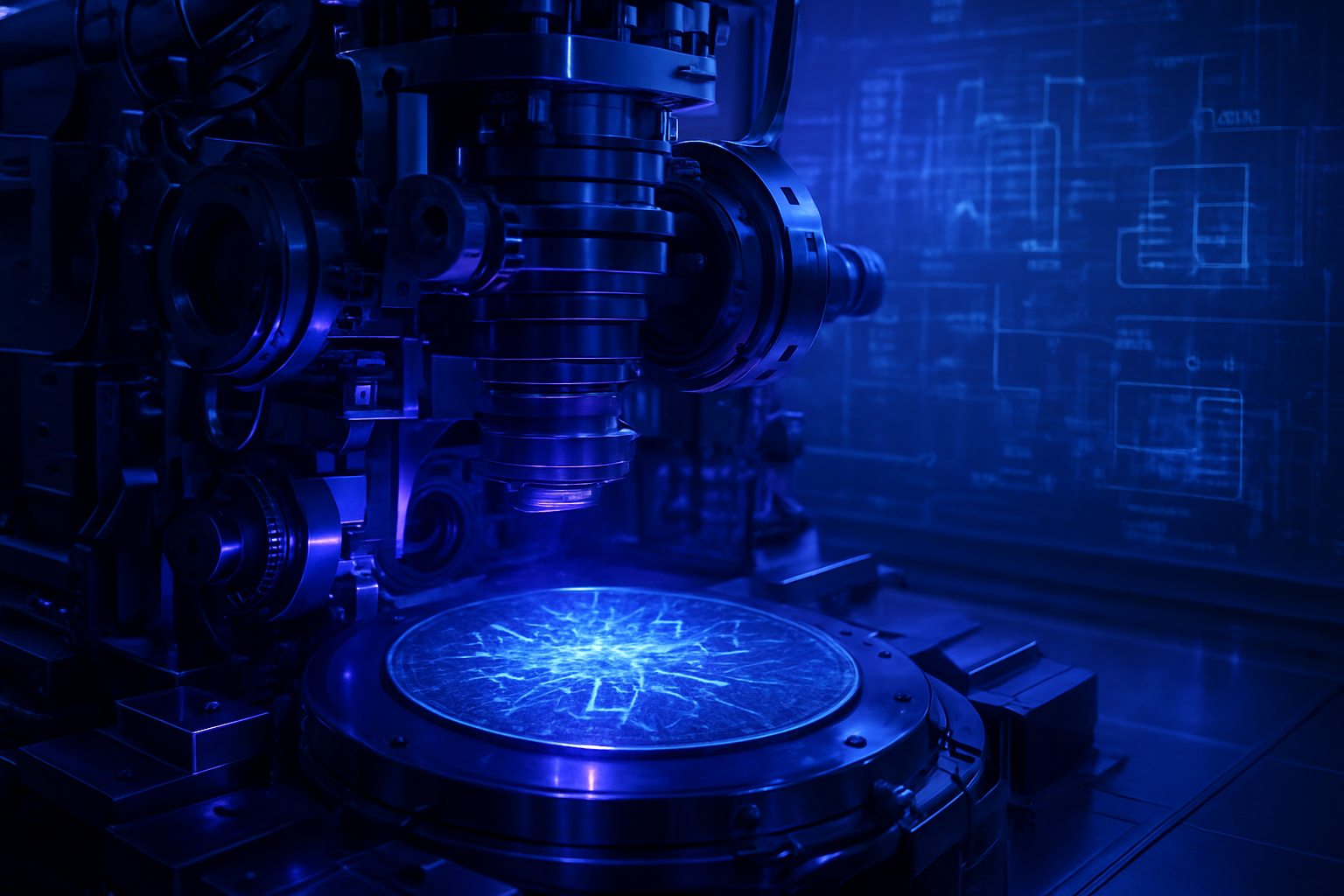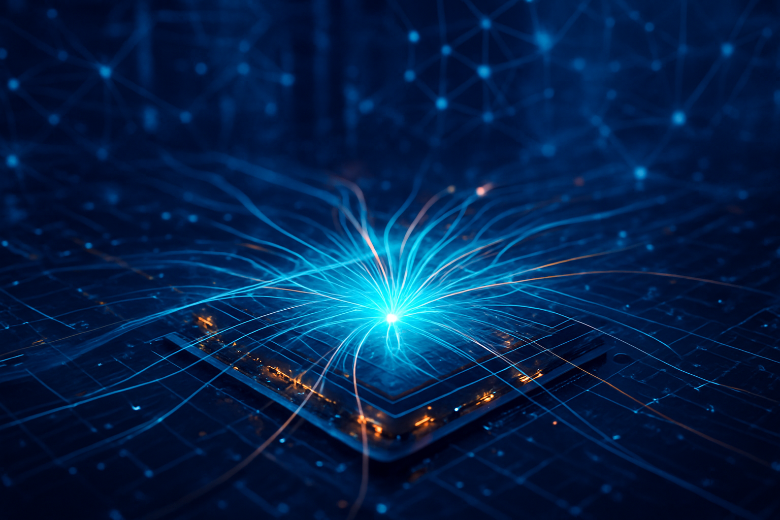
As of January 8, 2026, the semiconductor industry has reached a historic inflection point that promises to redefine the limits of artificial intelligence hardware. For decades, chip designers have struggled with a fundamental physical bottleneck: the "front-side" delivery of power, where power lines and signal wires compete for the same cramped real estate on top of transistors. Today, that bottleneck is being shattered as Backside Power Delivery (BSPD) officially enters high-volume manufacturing, led by Intel Corporation (NASDAQ: INTC) and its groundbreaking 18A process.
The shift to backside power—marketing-branded as "PowerVia" by Intel and "Super PowerRail" by Taiwan Semiconductor Manufacturing Company (NYSE: TSM)—is more than a mere manufacturing tweak; it is a fundamental architectural reorganization of the microchip. By moving the power delivery network to the underside of the silicon wafer, manufacturers are unlocking unprecedented levels of power efficiency and transistor density. This development arrives at a critical moment for the AI industry, where the ravenous energy demands of next-generation Large Language Models (LLMs) have threatened to outpace traditional hardware improvements.
The Technical Leap: Decoupling Power from Logic
Intel's 18A process, which reached high-volume manufacturing at Fab 52 in Chandler, Arizona, earlier this month, represents the first commercial deployment of Backside Power Delivery at scale. The core innovation, PowerVia, works by separating the intricate web of signal wires from the power delivery lines. In traditional chips, power must "tunnel" through up to 15 layers of metal interconnects to reach the transistors, leading to significant "voltage droop" and electrical interference. PowerVia eliminates this by routing power through the back of the wafer using Nano-Through Silicon Vias (nTSVs), providing a direct, low-resistance path to the transistors.
The technical specifications of Intel 18A are formidable. By implementing PowerVia alongside RibbonFET (Gate-All-Around) transistors, Intel has achieved a 30% reduction in voltage droop and a 6% boost in clock frequency at identical power levels compared to previous generations. More importantly for AI chip designers, the technology allows for 90% standard cell utilization, drastically reducing the "wiring congestion" that often forces engineers to leave valuable silicon area empty. This leap in logic density—exceeding 30% over the Intel 3 node—means more AI processing cores can be packed into the same physical footprint.
Initial reactions from the semiconductor research community have been overwhelmingly positive. Dr. Arati Prabhakar, Director of the White House Office of Science and Technology Policy, noted during a recent briefing that "the successful ramp of 18A is a validation of the 'five nodes in four years' strategy and a pivotal moment for domestic advanced manufacturing." Industry experts at SemiAnalysis have highlighted that Intel’s decision to decouple PowerVia from its first Gate-All-Around node (Intel 20A) allowed the company to de-risk the technology, giving them a roughly 18-month lead over TSMC in mastering the complexities of backside thinning and via alignment.
The Competitive Landscape: Intel’s First-Mover Advantage vs. TSMC’s A16 Response
The arrival of 18A has sent shockwaves through the foundry market, placing Intel Corporation (NASDAQ: INTC) in a rare position of technical leadership over TSMC. Intel has already secured major 18A commitments from Microsoft (NASDAQ: MSFT) and Amazon (NASDAQ: AMZN) for their custom AI accelerators, Maieutics and Trainium 3, respectively. By being the first to offer a mature BSPD solution, Intel Foundry is positioning itself as the premier destination for "AI-first" silicon, where thermal management and power delivery are the primary design constraints.
However, TSMC is not standing still. The world’s largest foundry is preparing its response in the form of the A16 node, scheduled for high-volume manufacturing in the second half of 2026. TSMC’s implementation, known as Super PowerRail, is technically more ambitious than Intel’s PowerVia. While Intel uses nTSVs to connect to the metal layers, TSMC’s Super PowerRail connects the power network directly to the source and drain of the transistors. This "direct-contact" approach is significantly harder to manufacture but is expected to offer an 8-10% speed increase and a 15-20% power reduction, potentially leapfrogging Intel’s performance metrics by late 2026.
The strategic battle lines are clearly drawn. Nvidia (NASDAQ: NVDA), the undisputed leader in AI hardware, has reportedly signed on as the anchor customer for TSMC’s A16 node to power its 2027 "Feynman" GPU architecture. Meanwhile, Apple (NASDAQ: AAPL) is rumored to be taking a more cautious approach, potentially skipping A16 for its mobile chips to focus on the N2P node, suggesting that backside power is currently viewed as a premium feature specifically optimized for high-performance computing and AI data centers rather than consumer mobile devices.
Wider Significance: Solving the AI Power Crisis
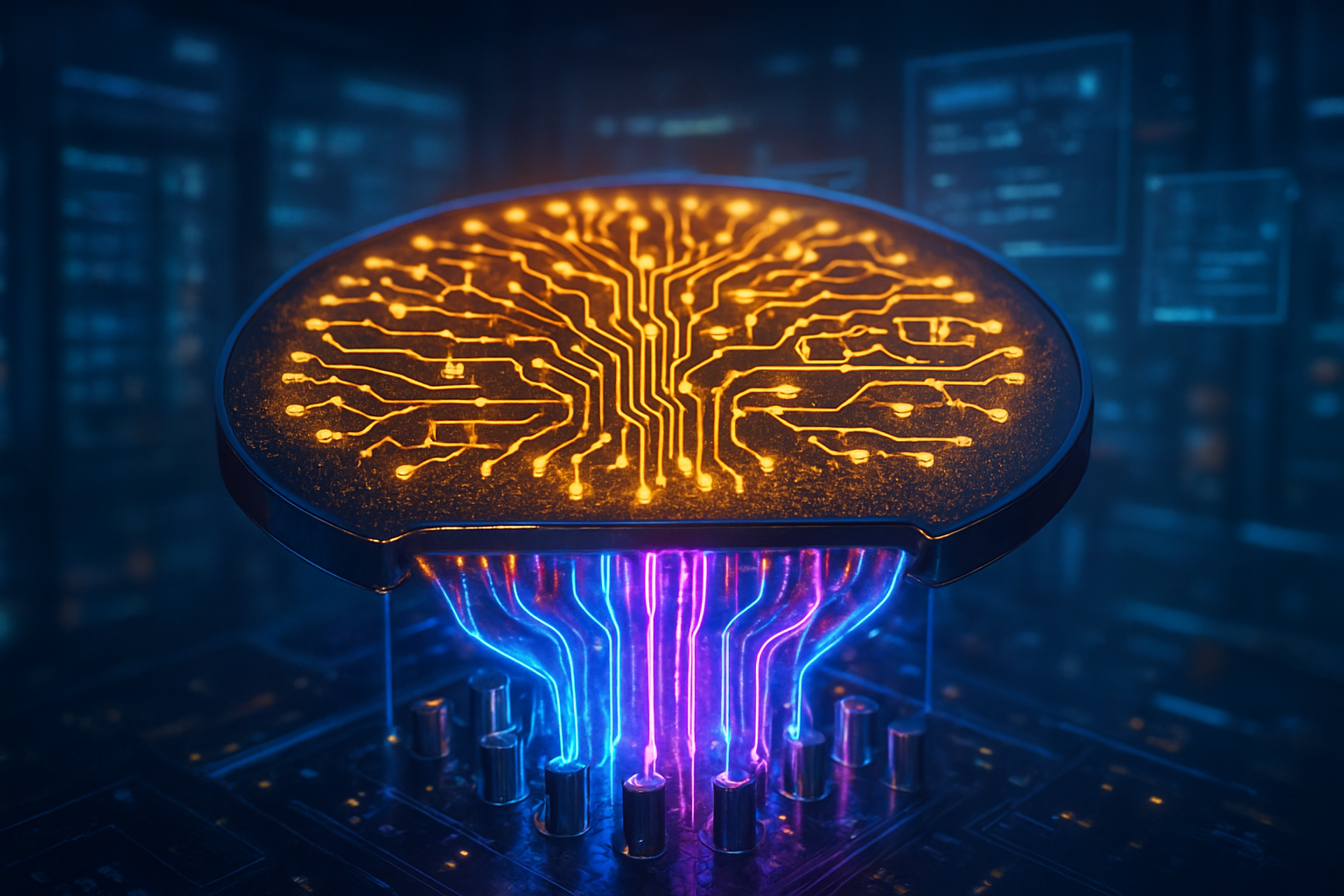
The transition to backside power delivery is a critical milestone in the broader AI landscape. As AI models grow in complexity, the "power wall"—the limit at which a chip can no longer be cooled or supplied with enough electricity—has become the primary obstacle to progress. BSPD effectively raises this wall. By reducing IR drop (voltage loss) and improving thermal dissipation, backside power allows AI accelerators to run at higher sustained workloads without throttling. This is essential for training the next generation of "Agentic AI" systems that require constant, high-intensity compute cycles.
Furthermore, this development marks the end of the "FinFET era" and the beginning of the "Angstrom era." The move to 18A and A16 represents a transition where traditional scaling (making things smaller) is being replaced by architectural scaling (rearranging how things are built). This shift mirrors previous milestones like the introduction of High-K Metal Gate (HKMG) or EUV lithography, both of which were necessary to keep Moore’s Law alive. In 2026, the "Backside Revolution" is the new prerequisite for remaining competitive in the global AI arms race.
There are, however, concerns regarding the complexity and cost of these new processes. Backside power requires extremely precise wafer thinning—grinding the silicon down to a fraction of its original thickness—and complex bonding techniques. These steps increase the risk of wafer breakage and lower initial yields. While Intel has reported healthy 18A yields in the 55-65% range, the high cost of these chips may further consolidate power in the hands of "Big Tech" giants like Alphabet (NASDAQ: GOOGL) and Meta (NASDAQ: META), who are the only ones capable of affording the multi-billion dollar design and fabrication costs associated with 1.6nm and 1.8nm silicon.
The Road Ahead: 1.4nm and the Future of AI Accelerators
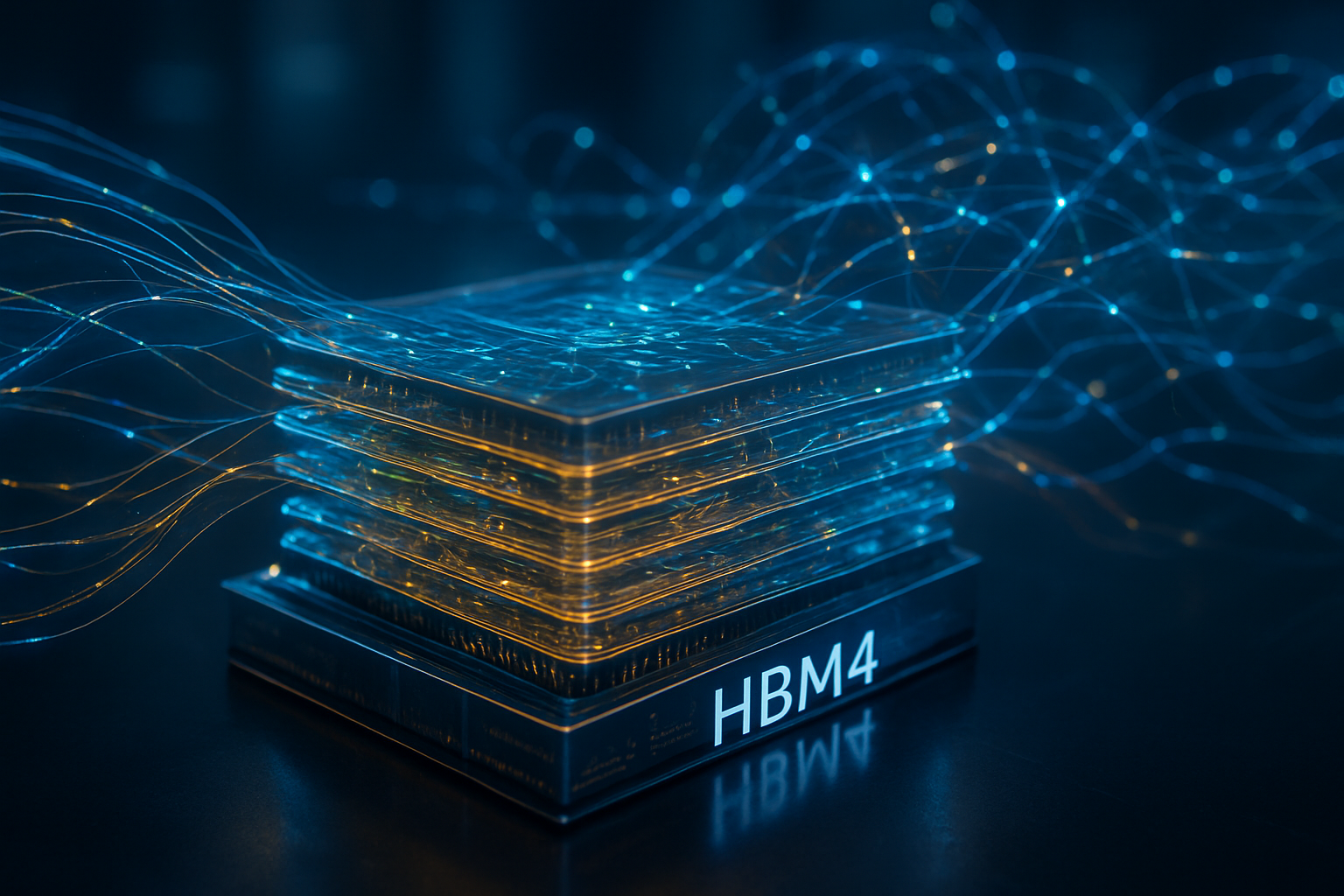
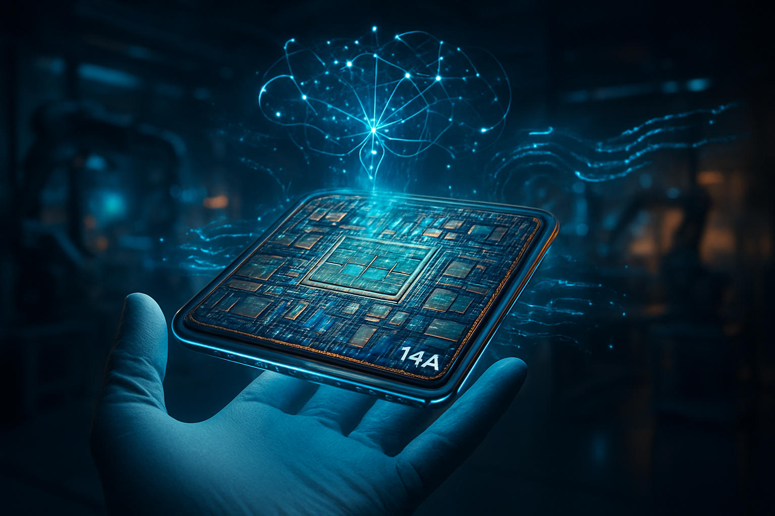
Looking toward the late 2020s, the trajectory of backside power is clear: it will become the standard for all high-performance logic. Intel is already planning its "14A" node for 2027, which will refine PowerVia with even denser interconnects. Simultaneously, Samsung Electronics (OTC: SSNLF) is preparing its SF2Z node for 2027, which will integrate its own version of BSPDN into its third-generation Gate-All-Around (MBCFET) architecture. Samsung’s entry will likely trigger a price war in the advanced foundry space, potentially making backside power more accessible to mid-sized AI startups and specialized ASIC designers.
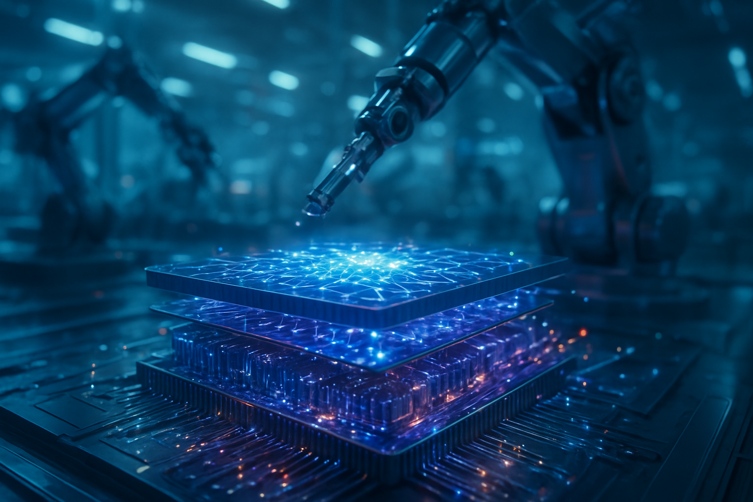
Beyond 2026, we expect to see "Backside Power 2.0," where manufacturers begin to move other components to the back of the wafer, such as decoupling capacitors or even certain types of memory (like RRAM). This could lead to "3D-stacked" AI chips where the logic is sandwiched between a backside power delivery layer and a front-side memory cache, creating a truly three-dimensional computing environment. The primary challenge remains the thermal density; as chips become more efficient at delivering power, they also become more concentrated heat sources, necessitating new liquid cooling or "on-chip" cooling technologies.
Conclusion: A New Foundation for Artificial Intelligence
The arrival of Intel’s 18A and the looming shadow of TSMC’s A16 mark the beginning of a new chapter in semiconductor history. Backside Power Delivery has transitioned from a laboratory curiosity to a commercial reality, providing the electrical foundation upon which the next decade of AI innovation will be built. By solving the "routing congestion" and "voltage droop" issues that have plagued chip design for years, PowerVia and Super PowerRail are enabling a new class of processors that are faster, cooler, and more efficient.
The significance of this development cannot be overstated. In the history of AI, we will look back at 2026 as the year the industry "flipped the chip" to keep the promise of exponential growth alive. For investors and tech enthusiasts, the coming months will be defined by the ramp-up of Intel’s Panther Lake and Clearwater Forest processors, providing the first real-world benchmarks of what backside power can do. As TSMC prepares its A16 risk production in the first half of 2026, the battle for silicon supremacy has never been more intense—or more vital to the future of technology.
This content is intended for informational purposes only and represents analysis of current AI developments.
TokenRing AI delivers enterprise-grade solutions for multi-agent AI workflow orchestration, AI-powered development tools, and seamless remote collaboration platforms.
For more information, visit https://www.tokenring.ai/.