Tag: Hardware

  • The Glass Frontier: Intel and Rapidus Lead the Charge into the Next Era of AI Hardware

    The Glass Frontier: Intel and Rapidus Lead the Charge into the Next Era of AI Hardware

    The transition to glass substrates is driven by the failure of organic materials (like ABF and BT resins) to cope with the extreme heat and structural demands of massive AI "superchips." Glass offers a Coefficient of Thermal Expansion (CTE) that closely matches that of silicon (3–7 ppm/°C), which drastically reduces the risk of warpage during the high-temperature manufacturing processes required for advanced 2nm and 1.4nm nodes. Furthermore, glass is an exceptional electrical insulator with significantly lower dielectric loss (Df) and a lower dielectric constant (Dk) than silicon-based interposers. This allows for signal speeds to double while cutting insertion loss in half—a critical requirement for the high-frequency data transfers essential for 5G, 6G, and ultra-fast AI training.

    Technically, the "magic" of glass lies in Through-Glass Vias (TGVs). These microscopic vertical interconnects allow for a 10-fold increase in interconnect density compared to traditional organic substrates. This density enables thousands of Input/Output (I/O) bumps, allowing multiple chiplets—CPUs, GPUs, and High Bandwidth Memory (HBM)—to be packed closer together with minimal latency. At SEMICON Japan in December 2025, Rapidus demonstrated the sheer scale of this potential by unveiling a 600mm x 600mm glass panel-level packaging (PLP) prototype. Unlike traditional 300mm round silicon wafers, these massive square panels can yield up to 10 times more interposers, significantly reducing material waste and enabling the creation of "monster" packages that can house up to 24 HBM4 dies alongside a multi-tile GPU.

    Market Dynamics: A High-Stakes Race for Dominance

    Intel is currently the undisputed leader in the "Glass War," having invested over a decade of R&D into the technology. The company's Arizona-based pilot line is already operational, and Intel is on track to integrate glass substrates into its high-volume manufacturing (HVM) roadmap by late 2026. This head start provides Intel with a significant strategic advantage, potentially allowing them to reclaim the lead in the foundry business by offering packaging capabilities that Taiwan Semiconductor Manufacturing Co. (NYSE: TSM) is not expected to match at scale until 2028 or 2029 with its "CoPoS" (Chip-on-Panel-on-Substrate) initiative.

    However, the competition is intensifying rapidly. Samsung Electronics (KRX: 005930) has fast-tracked its glass substrate development, leveraging its existing expertise in large-scale glass manufacturing from its display division. Samsung is currently building a pilot line at its Sejong facility and aims for a 2026-2027 rollout, potentially positioning itself as a primary alternative for AI giants like NVIDIA and Advanced Micro Devices (NASDAQ: AMD) who are desperate to diversify their supply chains away from a single source. Meanwhile, the emergence of Rapidus as a serious contender with its panel-level prototype suggests that the Japanese semiconductor ecosystem is successfully leveraging its legacy in LCD technology to leapfrog current packaging constraints.

    Redefining the AI Landscape and Moore’s Law

    The wider significance of glass substrates lies in their role as the "enabling platform" for the post-Moore's Law era. As it becomes increasingly difficult to shrink transistors further, the industry has turned to heterogeneous integration—stacking and stitching different chips together. Glass substrates provide the structural integrity needed to build these massive 3D structures. Intel’s stated goal of reaching 1 trillion transistors on a single package by 2030 is virtually impossible without the flatness and thermal stability provided by glass.

    This development also addresses the critical "power wall" in AI data centers. The extreme flatness of glass allows for more reliable implementation of Backside Power Delivery (such as Intel’s PowerVia technology) at the package level. This reduces power noise and improves overall energy efficiency by an estimated 15% to 20%. In an era where AI power consumption is a primary concern for hyperscalers and environmental regulators alike, the efficiency gains from glass substrates could be just as important as the performance gains.

    The Road to 2026 and Beyond

    Looking ahead, the next 12 to 18 months will be focused on solving the remaining engineering hurdles of glass: namely, fragility and handling. While glass is structurally superior once assembled, it is notoriously difficult to handle in a high-speed factory environment without cracking. Companies like Rapidus are working closely with equipment manufacturers to develop specialized "glass-safe" robotic handling systems and laser-drilling techniques for TGVs. If these challenges are met, the shift to 600mm square panels could drop the cost of manufacturing massive AI interposers by as much as 40% by 2027.

    In the near term, expect to see the first commercial glass-packaged chips appearing in high-end server environments. These will likely be specialized AI accelerators or high-end Xeon processors designed for the most demanding scientific computing tasks. As the ecosystem matures, we can anticipate the technology trickling down to consumer-grade high-end gaming GPUs and workstations, where thermal management is a constant struggle. The ultimate goal is a fully standardized glass-based ecosystem that allows for "plug-and-play" chiplet integration from various vendors.

    Conclusion: A New Foundation for Computing

    The move to glass substrates marks the beginning of a new chapter in semiconductor history. It is a transition that validates the industry's shift from "system-on-chip" to "system-in-package." By solving the thermal and density bottlenecks that have plagued organic substrates, Intel and Rapidus are paving the way for a new generation of AI hardware that was previously thought to be physically impossible.

    As we move into 2026, the industry will be watching closely to see if Intel can successfully execute its high-volume rollout and if Rapidus can translate its impressive prototype into a viable manufacturing reality. The stakes are immense; the winner of the glass substrate race will likely hold the keys to the world's most powerful AI systems for the next decade. For now, the "Glass War" is just beginning, and it promises to be the most consequential battle in the tech industry's ongoing evolution.


    This content is intended for informational purposes only and represents analysis of current AI developments.

    TokenRing AI delivers enterprise-grade solutions for multi-agent AI workflow orchestration, AI-powered development tools, and seamless remote collaboration platforms.
    For more information, visit https://www.tokenring.ai/.

  • HBM4 Wars: Samsung and SK Hynix Fast-Track the Future of AI Memory

    HBM4 Wars: Samsung and SK Hynix Fast-Track the Future of AI Memory

    The high-stakes race for semiconductor supremacy has entered a blistering new phase as the industry’s titans prepare for the "HBM4 Wars." With artificial intelligence workloads demanding unprecedented memory bandwidth, Samsung Electronics (KRX: 005930) and SK Hynix (KRX: 000660) have both officially fast-tracked their next-generation High Bandwidth Memory (HBM4) for mass production in early 2026. This acceleration, moving the timeline up by nearly six months from original projections, signals a desperate scramble to supply the hardware backbone for NVIDIA (NASDAQ: NVDA) and its upcoming "Rubin" GPU architecture.

    As of late December 2025, the rivalry between the two South Korean memory giants has shifted from incremental improvements to a fundamental architectural overhaul. HBM4 is not merely a faster version of its predecessor, HBM3e; it represents a paradigm shift where memory and logic manufacturing converge. With internal benchmarks showing performance leaps of up to 69% in end-to-end AI service delivery, the winner of this race will likely dictate the pace of AI evolution for the next three years.

    The 2,048-Bit Revolution: Breaking the Memory Wall

    The technical leap from HBM3e to HBM4 is the most significant in the technology's history. While HBM3e utilized a 1,024-bit interface, HBM4 doubles this to a 2,048-bit interface. This architectural change allows for massive increases in data throughput without requiring unsustainable increases in clock speeds. Samsung has reported internal test speeds reaching 11.7 Gbps per pin, while SK Hynix is targeting a steady 10 Gbps. These specifications translate to a staggering bandwidth of up to 2.8 TB/s per stack—nearly triple what was possible just two years ago.

    A critical innovation in HBM4 is the transition of the "base die"—the foundational layer of the memory stack—from a standard memory process to a high-performance logic process. SK Hynix has partnered with Taiwan Semiconductor Manufacturing Company (NYSE: TSM) to produce these logic dies using TSMC’s 5nm and 12nm FinFET nodes. In contrast, Samsung is leveraging its unique "turnkey" advantage, using its own 4nm logic foundry to manufacture the base die, memory cells, and advanced packaging in-house. This "one-stop-shop" approach aims to reduce latency and power consumption by up to 40% compared to HBM3e.

    Initial reactions from the AI research community have been overwhelmingly positive, particularly regarding the 16-high (16-Hi) stack configurations. These stacks will enable single GPUs to access up to 64GB of HBM4 memory, a necessity for the trillion-parameter Large Language Models (LLMs) that are becoming the industry standard. Industry experts note that the move to "buffer-less" HBM4 designs, which remove certain interface layers to save power and space, will be crucial for the next generation of mobile and edge AI applications.

    Strategic Alliances and the Battle for NVIDIA’s Rubin

    The immediate beneficiary of this memory war is NVIDIA, whose upcoming Rubin (R100) platform is designed specifically to harness HBM4. By securing early production slots for February 2026, NVIDIA ensures that its hardware will remain the undisputed leader in AI training and inference. However, the competitive landscape for the memory makers themselves is shifting. SK Hynix, which has long enjoyed a dominant position as NVIDIA’s primary HBM supplier, now faces a resurgent Samsung that has reportedly stabilized its 4nm yields at over 90%.

    For tech giants like Google (NASDAQ: GOOGL) and Meta (NASDAQ: META), the HBM4 fast-tracking offers a lifeline for their custom AI chip programs. Both companies are looking to diversify their supply chains away from a total reliance on NVIDIA, and the availability of HBM4 allows their proprietary TPUs and MTIA chips to compete on level ground. Meanwhile, Micron Technology (NASDAQ: MU) remains a formidable third player, though it is currently trailing slightly behind the aggressive 2026 mass production timelines set by its Korean rivals.

    The strategic advantage in this era will be defined by "custom HBM." Unlike previous generations where memory was a commodity, HBM4 is becoming a semi-custom product. Samsung’s ability to offer a hybrid model—using its own foundry or collaborating with TSMC for specific clients—positions it as a flexible partner for companies like Amazon (NASDAQ: AMZN) that require highly specific memory configurations for their data centers.

    The Broader AI Landscape: Sustaining the Intelligence Explosion

    The fast-tracking of HBM4 is a direct response to the "memory wall"—the phenomenon where processor speeds outpace the ability of memory to deliver data. In the broader AI landscape, this development is essential for the transition from generative text to multimodal AI and autonomous agents. Without the bandwidth provided by HBM4, the energy costs and latency of running advanced AI models would become economically unviable for most enterprises.

    However, this rapid advancement brings concerns regarding the environmental impact and the concentration of power within the "triangular alliance" of NVIDIA, TSMC, and the memory makers. The sheer power required to operate these HBM4-equipped clusters is immense, pushing data centers to adopt liquid cooling and more efficient power delivery systems. Furthermore, the complexity of 16-high HBM4 stacks introduces significant manufacturing risks; a single defect in one of the 16 layers can render the entire stack useless, leading to potential supply shocks if yields do not remain stable.

    Comparatively, the leap to HBM4 is being viewed as the "GPT-4 moment" for hardware. Just as GPT-4 redefined what was possible in software, HBM4 is expected to unlock a new tier of real-time AI capabilities, including high-fidelity digital twins and real-time global-scale translation services that were previously hindered by memory bottlenecks.

    Future Horizons: Beyond 2026 and the 16-Hi Frontier

    Looking beyond the initial 2026 rollout, the industry is already eyeing the development of HBM5 and "3D-stacked" memory-on-logic. The long-term goal is to move memory directly on top of the GPU compute dies, virtually eliminating the distance data must travel. While HBM4 uses advanced packaging like CoWoS (Chip-on-Wafer-on-Substrate), the next decade will likely see the total integration of these components into a single "AI super-chip."

    In the near term, the challenge remains the successful mass production of 16-high stacks. While 12-high stacks are the current target for early 2026, the "Rubin Ultra" variant expected in 2027 will demand the full 64GB capacity of 16-high HBM4. Experts predict that the first half of 2026 will be characterized by a "yield war," where the company that can most efficiently manufacture these complex vertical structures will capture the lion's share of the market.

    A New Chapter in Semiconductor History

    The acceleration of HBM4 marks a pivotal moment in the history of semiconductors. The traditional boundaries between memory and logic are dissolving, replaced by a collaborative ecosystem where foundries and memory makers must work in lockstep. Samsung’s aggressive comeback and SK Hynix’s established partnership with TSMC have created a duopoly that will drive the AI industry forward for the foreseeable future.

    As we head into 2026, the key indicators of success will be the first "Production Readiness Approval" (PRA) certificates from NVIDIA and the initial performance data from the first Rubin-based clusters. For the tech industry, the HBM4 wars are more than just a corporate rivalry; they are the primary engine of the AI revolution, ensuring that the silicon can keep up with the soaring ambitions of artificial intelligence.


    This content is intended for informational purposes only and represents analysis of current AI developments.

    TokenRing AI delivers enterprise-grade solutions for multi-agent AI workflow orchestration, AI-powered development tools, and seamless remote collaboration platforms.
    For more information, visit https://www.tokenring.ai/.

  • The 2nm Sprint: TSMC vs. Samsung in the Race for Next-Gen Silicon

    The 2nm Sprint: TSMC vs. Samsung in the Race for Next-Gen Silicon

    As of December 24, 2025, the semiconductor industry has reached a fever pitch in what analysts are calling the most consequential transition in the history of silicon manufacturing. The race to dominate the 2-nanometer (2nm) era is no longer a theoretical roadmap; it is a high-stakes reality. Taiwan Semiconductor Manufacturing Company (TSMC) (NYSE: TSM) has officially entered high-volume manufacturing (HVM) for its N2 process, while Samsung Electronics (KRX: 005930) is aggressively positioning its second-generation 2nm node (SF2P) to capture the exploding demand for artificial intelligence (AI) infrastructure and flagship mobile devices.

    This shift represents more than just a minor size reduction. It marks the industry's collective move toward Gate-All-Around (GAA) transistor architecture, a fundamental redesign of the transistor itself to overcome the physical limitations of the aging FinFET design. With AI server racks now demanding unprecedented power levels and flagship smartphones requiring more efficient on-device neural processing, the winner of this 2nm sprint will essentially dictate the pace of AI evolution for the remainder of the decade.

    The move to 2nm is defined by the transition from FinFET to GAAFET (Gate-All-Around Field-Effect Transistor) or "nanosheet" architecture. TSMC’s N2 process, which reached mass production in the fourth quarter of 2025, marks the company's first jump into nanosheets. By wrapping the gate around all four sides of the channel, TSMC has achieved a 10–15% speed improvement and a 25–30% reduction in power consumption compared to its 3nm (N3E) node. Initial yield reports for TSMC's N2 are remarkably strong, with internal data suggesting yields as high as 80% for early commercial batches, a feat attributed to the company's cautious, iterative approach to the new architecture.

    Samsung, conversely, is leveraging what it calls a "generational head start." Having introduced GAA technology at the 3nm stage, Samsung’s SF2 and its enhanced SF2P processes are technically third-generation GAA designs. This experience has allowed Samsung to offer Multi-Bridge Channel FET (MBCFET), which provides designers with greater flexibility to vary nanosheet widths to optimize for either extreme performance or ultra-low power. While Samsung’s yields have historically lagged behind TSMC’s, the company reported a breakthrough in late 2025, reaching a stable 60% yield for its SF2 node, which is currently powering the Exynos 2600 for the upcoming Galaxy S26 series.

    Industry experts have noted that the 2nm era also introduces "Backside Power Delivery" (BSPDN) as a critical secondary innovation. While TSMC has reserved its "Super Power Rail" for its enhanced N2P and A16 (1.6nm) nodes expected in late 2026, Intel (NASDAQ: INTC) has already pioneered this with its "PowerVia" technology on the 18A node. This separation of power and signal lines is essential for AI chips, as it drastically reduces "voltage droop," allowing chips to maintain higher clock speeds under the massive workloads required for Large Language Model (LLM) training.

    Initial reactions from the AI research community have been overwhelmingly focused on the thermal implications. At the 2nm level, power density has become so extreme that air cooling is increasingly viewed as obsolete for data center applications. The consensus among hardware architects is that 2nm AI accelerators, such as NVIDIA's (NASDAQ: NVDA) projected "Rubin" series, will necessitate a mandatory shift to direct-to-chip liquid cooling to prevent thermal throttling during intensive training cycles.

    The competitive landscape for 2nm is characterized by a fierce tug-of-war over the world's most valuable tech giants. TSMC remains the dominant force, with Apple (NASDAQ: AAPL) serving as its "alpha customer." Apple has reportedly secured nearly 50% of TSMC’s initial 2nm capacity for its A20 and A20 Pro chips, which will debut in the iPhone 18. This partnership ensures that Apple maintains its lead in on-device AI performance, providing the hardware foundation for more complex, autonomous Siri agents.

    However, Samsung is making strategic inroads by targeting the "Big Tech" hyperscalers. Samsung is currently running Multi-Project Wafer (MPW) sample tests with AMD (NASDAQ: AMD) for its second-generation SF2P node. AMD is reportedly pursuing a "dual-foundry" strategy, using TSMC for its Zen 6 "Venice" server CPUs while exploring Samsung’s 2nm for its next-generation Ryzen processors to mitigate supply chain risks. Similarly, Google (NASDAQ: GOOGL) is in deep negotiations with Samsung to produce its custom AI Tensor Processing Units (TPUs) at Samsung’s nearly completed facility in Taylor, Texas.

    Samsung’s Taylor fab has become a significant strategic advantage. Under Taiwan’s "N-2" policy, TSMC is required to keep its most advanced manufacturing technology in Taiwan for at least two years before exporting it to overseas facilities. This means TSMC’s Arizona plant will not produce 2nm chips until at least 2027. Samsung, however, is positioning its Texas fab as the only facility in the United States capable of mass-producing 2nm silicon in 2026. For US-based companies like Google and Meta (NASDAQ: META) that are under pressure to secure domestic supply chains, Samsung’s US-based 2nm capacity is an attractive alternative to TSMC’s Taiwan-centric production.

    Market dynamics are also being shaped by pricing. TSMC’s 2nm wafers are estimated to cost upwards of $30,000 each, a 50% increase over 3nm prices. Samsung has responded with an aggressive pricing model, reportedly undercutting TSMC by roughly 33%, with SF2 wafers priced near $20,000. This pricing gap is forcing many AI startups and second-tier chip designers to reconsider their loyalty to TSMC, potentially leading to a more fragmented and competitive foundry market.

    The significance of the 2nm transition extends far beyond corporate rivalry; it is a vital necessity for the survival of the AI boom. As LLMs scale toward tens of trillions of parameters, the energy requirements for training and inference have reached a breaking point. Gartner predicts that by 2027, nearly 40% of existing AI data centers will be operationally constrained by power availability. The 2nm node is the industry's primary weapon against this "power wall."

    By delivering a 30% reduction in power consumption, 2nm chips allow data center operators to pack more compute density into existing power envelopes. This is particularly critical for the transition from "Generative AI" to "Agentic AI"—autonomous systems that can reason and execute tasks in real-time. These agents require constant, low-latency background processing that would be prohibitively expensive and energy-intensive on 3nm or 5nm hardware. The efficiency of 2nm silicon is the "gating factor" that will determine whether AI agents become ubiquitous or remain limited to high-end enterprise applications.

    Furthermore, the 2nm era is coinciding with the integration of HBM4 (High Bandwidth Memory). The combination of 2nm logic and HBM4 is expected to provide over 15 TB/s of bandwidth, allowing massive models to fit into smaller GPU clusters. This reduces the communication latency that currently plagues large-scale AI training. Compared to the 7nm milestone that enabled the first wave of deep learning, or the 5nm node that powered the ChatGPT explosion, the 2nm breakthrough is being viewed as the "efficiency milestone" that makes AI economically sustainable at a global scale.

    However, the move to 2nm also raises concerns regarding the "Economic Wall." As wafer costs soar, the barrier to entry for custom silicon is rising. Only the wealthiest corporations can afford to design and manufacture at 2nm, potentially leading to a concentration of AI power among a handful of "Silicon Superpowers." This has prompted a surge in chiplet-based designs, where only the most critical compute dies are built on 2nm, while less sensitive components remain on older, cheaper nodes.

    Looking ahead, the 2nm sprint is merely a precursor to the 1.4nm (A14) era. Both TSMC and Samsung have already begun outlining their 1.4nm roadmaps, with production targets set for 2027 and 2028. These future nodes will rely heavily on High-NA (Numerical Aperture) Extreme Ultraviolet (EUV) lithography, a next-generation manufacturing technology that allows for even finer circuit patterns. Intel has already taken delivery of the world’s first High-NA EUV machines, signaling that the three-way battle for silicon supremacy will only intensify.

    In the near term, the industry is watching for the first 2nm-powered AI accelerators to hit the market in mid-2026. These chips are expected to enable "World Models"—AI systems that can simulate physical reality with high fidelity, a prerequisite for advanced robotics and autonomous vehicles. The challenge remains the complexity of the manufacturing process; as transistors approach the size of a few dozen atoms, quantum tunneling and other physical anomalies become increasingly difficult to manage.

    Predicting the next phase, analysts suggest that the focus will shift from raw transistor density to "System-on-Wafer" technologies. Rather than individual chips, foundries may begin producing entire wafers as single, interconnected AI processing units. This would eliminate the bottlenecks of traditional chip packaging, but it requires the near-perfect yields that TSMC and Samsung are currently fighting to achieve at the 2nm level.

    The 2nm sprint represents a pivotal moment in the history of computing. TSMC’s successful entry into high-volume manufacturing with its N2 node secures its position as the industry’s reliable powerhouse, while Samsung’s aggressive testing of its second-generation GAA process and its strategic US-based production in Texas offer a compelling alternative for a geopolitically sensitive world. The key takeaways from this race are clear: the architecture of the transistor has changed forever, and the energy efficiency of 2nm silicon is now the primary currency of the AI era.

    In the context of AI history, the 2nm breakthrough will likely be remembered as the point where hardware finally began to catch up with the soaring ambitions of software architects. It provides the thermal and electrical headroom necessary for the next generation of autonomous agents and trillion-parameter models to move from research labs into the pockets and desktops of billions of users.

    In the coming weeks and months, the industry will be watching for the first production samples from Samsung’s Taylor fab and the final performance benchmarks of Apple’s A20 silicon. As the first 2nm chips begin to roll off the assembly lines, the race for next-gen silicon will move from the cleanrooms of Hsinchu and Pyeongtaek to the data centers and smartphones that define modern life. The sprint is over; the 2nm era has begun.


    This content is intended for informational purposes only and represents analysis of current AI developments.

    TokenRing AI delivers enterprise-grade solutions for multi-agent AI workflow orchestration, AI-powered development tools, and seamless remote collaboration platforms.
    For more information, visit https://www.tokenring.ai/.

  • The Silicon Wall: How 2nm CMOS and Backside Power are Saving the AI Revolution

    The Silicon Wall: How 2nm CMOS and Backside Power are Saving the AI Revolution

    As of December 19, 2025, the semiconductor industry has reached a definitive crossroads where the traditional laws of physics and the insatiable demands of artificial intelligence have finally collided. For decades, "Moore’s Law" was sustained by simply shrinking transistors on a two-dimensional plane, but the era of Large Language Models (LLMs) has pushed these classical manufacturing processes to their absolute breaking point. To prevent a total stagnation in AI performance, the world’s leading foundries have been forced to reinvent the very architecture of the silicon chip, moving from the decades-old FinFET design to radical new "Gate-All-Around" (GAA) structures and innovative power delivery systems.

    This transition marks the most significant shift in microchip fabrication since the 1960s. As trillion-parameter models become the industry standard, the bottleneck is no longer just raw compute power, but the physical ability to deliver electricity to billions of transistors and dissipate the resulting heat without melting the silicon. The rollout of 2-nanometer (2nm) class nodes by late 2025 represents a "hail mary" for the AI industry, utilizing atomic-scale engineering to keep the promise of exponential intelligence alive.

    The Death of the Fin: GAAFET and the 2nm Frontier

    The technical centerpiece of this evolution is the industry-wide abandonment of the FinFET (Fin Field-Effect Transistor) in favor of Gate-All-Around (GAA) technology. In traditional FinFETs, the gate controlled the channel from three sides; however, at the 2nm scale, electrons began "leaking" out of the channel due to quantum tunneling, leading to massive power waste. The new GAA architecture—referred to as "Nanosheets" by TSMC (NYSE:TSM), "RibbonFET" by Intel (NASDAQ:INTC), and "MBCFET" by Samsung (KRX:005930)—wraps the gate entirely around the channel on all four sides. This provides total electrostatic control, allowing for higher clock speeds at lower voltages, which is essential for the high-duty-cycle matrix multiplications required by LLM inference.

    Beyond the transistor itself, the most disruptive technical advancement of 2025 is Backside Power Delivery (BSPDN). Historically, chips were built like a house where the plumbing and electrical wiring were all crammed into the ceiling, creating a congested mess that blocked the "residents" (the transistors) from moving efficiently. Intel’s "PowerVia" and TSMC’s "Super Power Rail" have moved the entire power distribution network to the bottom of the silicon wafer. This decoupling of power and signal lines reduces voltage drops by up to 30% and frees up the top layers for the ultra-fast data interconnects that AI clusters crave.

    Initial reactions from the AI research community have been overwhelmingly positive, though tempered by the sheer cost of these advancements. High-NA (Numerical Aperture) EUV lithography machines from ASML (NASDAQ:ASML), which are required to print these 2nm features, now cost upwards of $380 million each. Experts note that while these technologies solve the immediate "Power Wall," they introduce a new "Economic Wall," where only the largest hyperscalers can afford to design and manufacture the cutting-edge silicon necessary for next-generation frontier models.

    The Foundry Wars: Who Wins the AI Hardware Race?

    This technological shift has fundamentally rewired the competitive landscape for tech giants. NVIDIA (NASDAQ:NVDA) remains the primary beneficiary, as its upcoming "Rubin" R100 architecture is the first to fully leverage TSMC’s 2nm N2 process and advanced CoWoS-L (Chip-on-Wafer-on-Substrate) packaging. By stitching together multiple 2nm compute dies with the newly standardized HBM4 memory, NVIDIA has managed to maintain its lead in training efficiency, making it difficult for competitors to catch up on a performance-per-watt basis.

    However, the 2nm era has also provided a massive opening for Intel. After years of trailing, Intel’s 18A (1.8nm) node has entered high-volume manufacturing at its Arizona fabs, successfully integrating both RibbonFET and PowerVia ahead of its rivals. This has allowed Intel to secure major foundry customers like Microsoft (NASDAQ:MSFT) and Amazon (NASDAQ:AMZN), who are increasingly looking to design their own custom AI ASICs (Application-Specific Integrated Circuits) to reduce their reliance on NVIDIA. The ability to offer "system-level" foundry services—combining 1.8nm logic with advanced 3D packaging—has positioned Intel as a formidable challenger to TSMC’s long-standing dominance.

    For startups and mid-tier AI companies, the implications are more double-edged. While the increased efficiency of 2nm chips may eventually lower the cost of API tokens for models like GPT-5 or Claude 4, the "barrier to entry" for building custom hardware has never been higher. The industry is seeing a consolidation of power, where the strategic advantage lies with companies that can secure guaranteed capacity at 2nm fabs. This has led to a flurry of long-term supply agreements and "pre-payments" for fab space, effectively turning silicon capacity into a form of geopolitical and corporate currency.

    Beyond the Transistor: The Memory Wall and Sustainability

    The evolution of CMOS for AI is not occurring in a vacuum; it is part of a broader trend toward "System-on-Package" (SoP) design. As transistors hit physical limits, the "Memory Wall"—the speed gap between the processor and the RAM—has become the primary bottleneck for LLMs. The response in 2025 has been the rapid adoption of HBM4 (High Bandwidth Memory), developed by leaders like SK Hynix (KRX:000660) and Micron (NASDAQ:MU). HBM4 utilizes a 2048-bit interface to provide over 2 terabytes per second of bandwidth, but it requires the same advanced packaging techniques used for 2nm logic, further blurring the line between chip design and manufacturing.

    There are, however, significant concerns regarding the environmental impact of this hardware arms race. While 2nm chips are more power-efficient per operation, the sheer scale of the deployments means that total AI energy consumption continues to skyrocket. The manufacturing process for 2nm wafers is also significantly more water-and-chemical-intensive than previous generations. Critics argue that the industry is "running to stand still," using massive amounts of resources to achieve incremental gains in model performance that may eventually face diminishing returns.

    Comparatively, this milestone is being viewed as the "Post-Silicon Era" transition. Much like the move from vacuum tubes to transistors, or from planar transistors to FinFETs, the shift to GAA and Backside Power represents a fundamental change in the building blocks of computation. It marks the moment when "Moore's Law" transitioned from a law of physics to a law of sophisticated 3D engineering and material science.

    The Road to 14A and Glass Substrates

    Looking ahead, the roadmap for AI silicon is already moving toward the 1.4nm (14A) node, expected to arrive around 2027. Experts predict that the next major breakthrough will involve the replacement of organic packaging materials with glass substrates. Companies like Intel and SK Absolics are currently piloting glass cores, which offer superior thermal stability and flatness. This will allow for even larger "gigascale" packages that can house dozens of chiplets and HBM stacks, essentially creating a "supercomputer on a single substrate."

    Another area of intense research is the use of alternative metals like Ruthenium and Molybdenum for chip wiring. As copper wires become too thin and resistive at the 2nm level, these exotic metals will be required to keep signals moving at the speed of light. The challenge will be integrating these materials into the existing CMOS workflow without tanking yields. If successful, these developments could pave the way for AGI-scale hardware capable of trillion-parameter real-time reasoning.

    Summary and Final Thoughts

    The evolution of CMOS technology in late 2025 serves as a testament to human ingenuity in the face of physical limits. By transitioning to GAAFET architectures, implementing Backside Power Delivery, and embracing HBM4, the semiconductor industry has successfully extended the life of Moore’s Law for at least another decade. The key takeaway is that AI development is no longer just a software or algorithmic challenge; it is a deep-tech manufacturing challenge that requires the tightest possible integration between silicon design and fabrication.

    In the history of AI, the 2nm transition will likely be remembered as the moment hardware became the ultimate gatekeeper of progress. While the performance gains are staggering, the concentration of this technology in the hands of a few global foundries and hyperscalers will continue to be a point of contention. In the coming weeks and months, the industry will be watching the yield rates of TSMC’s N2 and Intel’s 18A nodes closely, as these numbers will ultimately determine the pace of AI innovation through 2026 and beyond.


    This content is intended for informational purposes only and represents analysis of current AI developments.

    TokenRing AI delivers enterprise-grade solutions for multi-agent AI workflow orchestration, AI-powered development tools, and seamless remote collaboration platforms.
    For more information, visit https://www.tokenring.ai/.

  • The Great Silicon Deconstruction: How Chiplets Are Breaking the Physical Limits of AI

    The Great Silicon Deconstruction: How Chiplets Are Breaking the Physical Limits of AI

    The semiconductor industry has reached a historic inflection point in late 2025, marking the definitive end of the "Big Iron" era of monolithic chip design. For decades, the goal of silicon engineering was to cram as many transistors as possible onto a single, continuous slab of silicon. However, as artificial intelligence models have scaled into the tens of trillions of parameters, the physical and economic limits of this "monolithic" approach have finally shattered. In its place, a modular revolution has taken hold: the shift to chiplet architectures.

    This transition represents a fundamental reimagining of how computers are built. Rather than a single massive processor, modern AI accelerators like the NVIDIA (NASDAQ: NVDA) Rubin and AMD (NASDAQ: AMD) Instinct MI400 are now constructed like high-tech LEGO sets. By breaking a processor into smaller, specialized "chiplets"—some for intense mathematical calculation, others for memory management or high-speed data transfer—manufacturers are overcoming the "reticle limit," the physical boundary of how large a single chip can be printed. This modularity is not just a technical curiosity; it is the primary engine allowing AI performance to continue doubling even as traditional Moore’s Law scaling slows to a crawl.

    Breaking the Reticle Limit: The Physics of Modular Silicon

    The technical catalyst for the chiplet shift is the "reticle limit," a physical constraint of lithography machines that prevents them from printing a single chip larger than approximately 858mm². As of late 2025, the demand for AI compute has far outstripped what can fit within that tiny square. To solve this, manufacturers are using advanced packaging techniques like TSMC (NYSE: TSM) CoWoS-L (Chip-on-Wafer-on-Substrate with Local Silicon Interconnect) to "stitch" multiple dies together. The recently unveiled NVIDIA Rubin architecture, for instance, effectively creates a "4x reticle" footprint, enabling a level of compute density that would be physically impossible to manufacture as a single piece of silicon.

    Beyond sheer size, the move to chiplets has solved the industry’s most pressing economic headache: yield rates. In a monolithic 3nm design, a single microscopic defect can ruin an entire $10,000 chip. By disaggregating the design into smaller chiplets, manufacturers can test each module individually as a "Known Good Die" (KGD) before assembly. This has pushed effective manufacturing yields for top-tier AI accelerators from the 50-60% range seen in 2023 to over 85% today. If one small chiplet is defective, only that tiny piece is discarded, drastically reducing waste and stabilizing the astronomical costs of leading-edge semiconductor fabrication.

    Furthermore, chiplets enable "heterogeneous integration," allowing engineers to mix and match different manufacturing processes within the same package. In a 2025-era AI processor, the core "brain" might be built on an expensive, ultra-efficient 2nm or 3nm node, while the less-sensitive I/O and memory controllers remain on more mature, cost-effective 5nm or 7nm nodes. This "node optimization" ensures that every dollar of capital expenditure is directed toward the components that provide the greatest performance benefit, preventing a total collapse of the price-to-performance ratio in the AI sector.

    Initial reactions from the AI research community have been overwhelmingly positive, particularly regarding the integration of HBM4 (High Bandwidth Memory). By stacking memory chiplets directly on top of or adjacent to the compute dies, manufacturers are finally bridging the "memory wall"—the bottleneck where processors sit idle while waiting for data. Experts at the 2025 IEEE International Solid-State Circuits Conference noted that this modular approach has enabled a 400% increase in memory bandwidth over the last two years, a feat that would have been unthinkable under the old monolithic paradigm.

    Strategic Realignment: Hyperscalers and the Custom Silicon Moat

    The chiplet revolution has fundamentally altered the competitive landscape for tech giants and AI labs. No longer content to be mere customers of the major chipmakers, hyperscalers like Amazon (NASDAQ: AMZN), Alphabet (NASDAQ: GOOGL), and Meta (NASDAQ: META) have become architects of their own modular silicon. Amazon’s recently launched Trainium3, for example, utilizes a dual-chiplet design that allows AWS to offer AI training credits at nearly 60% lower costs than traditional GPU instances. By using chiplets to lower the barrier to entry for custom hardware, these companies are building a "silicon moat" that optimizes their specific internal workloads, such as recommendation engines or large language model (LLM) inference.

    For established chipmakers, the transition has sparked a fierce strategic battle over packaging dominance. While NVIDIA (NASDAQ: NVDA) remains the performance king with its Rubin and Blackwell platforms, Intel (NASDAQ: INTC) has leveraged its Foveros 3D packaging technology to secure massive foundry wins, including Microsoft (NASDAQ: MSFT) and its Maia 200 series. Intel’s ability to offer "Secure Enclave" manufacturing within the United States has become a significant strategic advantage as geopolitical tensions continue to cloud the future of the global supply chain. Meanwhile, Samsung (KRX: 005930) has positioned itself as a "one-stop shop," integrating its own HBM4 memory with proprietary 2.5D packaging to offer a vertically integrated alternative to the TSMC-NVIDIA duopoly.

    The disruption extends to the startup ecosystem as well. The maturation of the UCIe 3.0 (Universal Chiplet Interconnect Express) standard has created a "Chiplet Economy," where smaller hardware startups like Tenstorrent and Etched can buy "off-the-shelf" I/O and memory chiplets. This allows them to focus their limited R&D budgets on designing a single, high-value AI logic chiplet rather than an entire complex SoC. This democratization of hardware design has reduced the capital required for a first-generation tape-out by an estimated 40%, leading to a surge in specialized AI hardware tailored for niche applications like edge robotics and medical diagnostics.

    The Wider Significance: A New Era for Moore’s Law

    The shift to chiplets is more than a manufacturing tweak; it is the birth of "Moore’s Law 2.0." While the physical shrinking of transistors is reaching its atomic limit, the ability to scale systems through modularity provides a new path forward for the AI landscape. This trend fits into the broader move toward "system-level" scaling, where the unit of compute is no longer a single chip or even a single server, but the entire data center rack. As we move through the end of 2025, the industry is increasingly viewing the data center as one giant, disaggregated computer, with chiplets serving as the interchangeable components of its massive brain.

    However, this transition is not without concerns. The complexity of testing and assembling multi-die packages is immense, and the industry’s heavy reliance on TSMC (NYSE: TSM) for advanced packaging remains a significant single point of failure. Furthermore, as chips become more modular, the power density within a single package has skyrocketed, leading to unprecedented thermal management challenges. The shift toward liquid cooling and even co-packaged optics is no longer a luxury but a requirement for the next generation of AI infrastructure.

    Comparatively, the chiplet milestone is being viewed by industry historians as significant as the transition from vacuum tubes to transistors, or the move from single-core to multi-core CPUs. It represents a shift from a "fixed" hardware mindset to a "fluid" one, where hardware can be as iterative and modular as the software it runs. This flexibility is crucial in a world where AI models are evolving faster than the 18-to-24-month design cycle of traditional semiconductors.

    The Horizon: Glass Substrates and Optical Interconnects

    Looking toward 2026 and beyond, the industry is already preparing for the next phase of the chiplet evolution. One of the most anticipated near-term developments is the commercialization of glass core substrates. Led by research from Intel (NASDAQ: INTC) and TSMC (NYSE: TSM), glass offers superior flatness and thermal stability compared to the organic materials used today. This will allow for even larger package sizes, potentially accommodating up to 12 or 16 HBM4 stacks on a single interposer, further pushing the boundaries of memory capacity for the next generation of "Super-LLMs."

    Another frontier is the integration of Co-Packaged Optics (CPO). As data moves between chiplets, traditional electrical signals generate significant heat and consume a large portion of the chip’s power budget. Experts predict that by late 2026, we will see the first widespread use of optical chiplets that use light rather than electricity to move data between dies. This would effectively eliminate the "communication wall," allowing for near-instantaneous data transfer across a rack of thousands of chips, turning a massive cluster into a single, unified compute engine.

    The challenges ahead are primarily centered on standardization and software. While UCIe has made great strides, ensuring that a chiplet from one vendor can talk seamlessly to a chiplet from another remains a hurdle. Additionally, compilers and software stacks must become "chiplet-aware" to efficiently distribute workloads across these fragmented architectures. Nevertheless, the trajectory is clear: the future of AI is modular.

    Conclusion: The Modular Future of Intelligence

    The shift from monolithic to chiplet architectures marks the most significant architectural change in the semiconductor industry in decades. By overcoming the physical limits of lithography and the economic barriers of declining yields, chiplets have provided the runway necessary for the AI revolution to continue its exponential growth. The success of platforms like NVIDIA’s Rubin and AMD’s MI400 has proven that the "LEGO-like" approach to silicon is not just viable, but essential for the next decade of compute.

    As we look toward 2026, the key takeaways are clear: packaging is the new Moore’s Law, custom silicon is the new strategic moat for hyperscalers, and the "deconstruction" of the data center is well underway. The industry has moved from asking "how small can we make a chip?" to "how many pieces can we connect?" This change in perspective ensures that while the physical limits of silicon may be in sight, the limits of artificial intelligence remain as distant as ever. In the coming months, watch for the first high-volume deployments of HBM4 and the initial pilot programs for glass substrates—these will be the bellwethers for the next stage of the modular era.


    This content is intended for informational purposes only and represents analysis of current AI developments.

    TokenRing AI delivers enterprise-grade solutions for multi-agent AI workflow orchestration, AI-powered development tools, and seamless remote collaboration platforms.
    For more information, visit https://www.tokenring.ai/.

  • The Silicon Bedrock: Strengthening Forecasts for AI Chip Equipment Signal a Multi-Year Infrastructure Supercycle

    The Silicon Bedrock: Strengthening Forecasts for AI Chip Equipment Signal a Multi-Year Infrastructure Supercycle

    As 2025 draws to a close, the semiconductor industry is witnessing a historic shift in capital allocation, driven by a "giga-cycle" of investment in artificial intelligence infrastructure. According to the latest year-end reports from industry authority SEMI and leading equipment manufacturers, global Wafer Fab Equipment (WFE) spending is forecast to hit a record-breaking $145 billion in 2026. This surge is underpinned by an insatiable demand for next-generation AI processors and high-bandwidth memory, forcing a radical retooling of the world’s most advanced fabrication facilities.

    The immediate significance of this development cannot be overstated. We are moving past the era of "AI experimentation" into a phase of "AI industrialization," where the physical limits of silicon are being pushed by revolutionary new architectures. Leaders in the space, most notably Applied Materials (NASDAQ: AMAT), have reported record annual revenues of over $28 billion for fiscal 2025, with visibility into customer factory plans extending well into 2027. This strengthening forecast suggests that the "pick and shovel" providers of the AI gold rush are entering their most profitable era yet, as the industry races toward a $1 trillion total market valuation by 2026.

    The Architecture of Intelligence: GAA, High-NA, and Backside Power

    The technical backbone of this 2026 supercycle rests on three primary architectural inflections: Gate-All-Around (GAA) transistors, Backside Power Delivery (BSPDN), and High-NA EUV lithography. Unlike the FinFET transistors that dominated the last decade, GAA nanosheets wrap the gate around all four sides of the channel, providing superior control over current leakage and enabling the jump to 2nm and 1.4nm process nodes. Applied Materials has positioned itself as the dominant force here, capturing over 50% market share in GAA-specific equipment, including the newly unveiled Centura Xtera Epi system, which is critical for the epitaxial growth required in these complex 3D structures.

    Simultaneously, the industry is adopting Backside Power Delivery, a radical redesign that moves the power distribution network to the rear of the silicon wafer. This decoupling of power and signal routing significantly reduces voltage drop and clears "routing congestion" on the front side, allowing for denser, more energy-efficient AI chips. To inspect these buried structures, the industry has turned to advanced metrology tools like the PROVision 10 eBeam from Applied Materials, which can "see" through multiple layers of silicon to ensure alignment at the atomic scale.

    Furthermore, the long-awaited era of High-NA (Numerical Aperture) EUV lithography has officially transitioned from the lab to the fab. As of December 2025, ASML (NASDAQ: ASML) has confirmed that its EXE:5200 series machines have completed acceptance testing at Intel (NASDAQ: INTC) and are being delivered to Samsung (KRX: 005930) for 2nm mass production. These €350 million machines allow for finer resolution than ever before, eliminating the need for complex multi-patterning steps and streamlining the production of the massive die sizes required for next-gen AI accelerators like Nvidia’s upcoming Rubin architecture.

    The Equipment Giants: Strategic Advantages and Market Positioning

    The strengthening forecasts have created a clear hierarchy of beneficiaries among the "Big Five" equipment makers. Applied Materials (NASDAQ: AMAT) has successfully pivoted its business model, reducing its exposure to the volatile Chinese market while doubling down on materials engineering for advanced packaging. By dominating the "die-to-wafer" hybrid bonding market with its Kinex system, AMAT is now essential for the production of High-Bandwidth Memory (HBM4), which is expected to see a massive ramp-up in the second half of 2026.

    Lam Research (NASDAQ: LRCX) has similarly fortified its position through its Cryo 3.0 cryogenic etching technology. Originally designed for 3D NAND, this technology has become a bottleneck-breaker for HBM4 production. By etching through-silicon vias (TSVs) at temperatures as low as -80°C, Lam’s tools can achieve near-perfect vertical profiles at 2.5 times the speed of traditional methods. This efficiency is vital as memory makers like SK Hynix (KRX: 000660) report that their 2026 HBM4 capacity is already fully committed to major AI clients.

    For the fabless giants and foundries, these developments represent both an opportunity and a strategic risk. While Nvidia (NASDAQ: NVDA) and Advanced Micro Devices (NASDAQ: AMD) stand to benefit from the higher performance of 2nm GAA chips, they are increasingly dependent on the production yields of TSMC (NYSE: TSM). The market is closely watching whether the equipment providers can deliver enough tools to meet TSMC’s projected 60% expansion in CoWoS (Chip-on-Wafer-on-Substrate) packaging capacity. Any delay in tool delivery could create a multi-billion dollar revenue gap for the entire AI ecosystem.

    Geopolitics, Energy, and the $1 Trillion Milestone

    The wider significance of this equipment boom extends into the realms of global energy and geopolitics. The shift toward "Sovereign AI"—where nations build their own domestic compute clusters—has decentralized demand. Equipment that was once destined for a few mega-fabs in Taiwan and Korea is now being shipped to new "greenfield" projects in the United States, Japan, and Europe, funded by initiatives like the U.S. CHIPS Act. This geographic diversification is acting as a hedge against regional instability, though it introduces new logistical complexities for equipment maintenance and talent.

    Energy efficiency has also emerged as a primary driver for hardware upgrades. As data center power consumption becomes a political and environmental flashpoint, the transition to Backside Power and GAA transistors is being framed as a "green" necessity. Analysts from Gartner and IDC suggest that while generative AI software may face a "trough of disillusionment" in 2026, the demand for the underlying hardware will remain robust because these newer, more efficient chips are required to make AI economically viable at scale.

    However, the industry is not without its concerns. Experts point to a potential "HBM4 capacity crunch" and the massive power requirements of the 2026 data center build-outs as major friction points. If the electrical grid cannot support the 1GW+ data centers currently on the drawing board, the demand for the chips produced by these expensive new machines could soften. Furthermore, the "small yard, high fence" trade policies of late 2025 continue to cast a shadow over the global supply chain, with new export controls on metrology and lithography components remaining a top-tier risk for CEOs.

    Looking Ahead: The Road to 1.4nm and Optical Interconnects

    Looking beyond 2026, the roadmap for AI chip equipment is already focusing on the 1.4nm node (often referred to as A14). This will likely involve even more exotic materials and the potential integration of optical interconnects directly onto the silicon die. Companies are already prototyping "Silicon Photonics" equipment that would allow chips to communicate via light rather than electricity, potentially solving the "memory wall" that currently limits AI training speeds.

    In the near term, the industry will focus on perfecting "heterogeneous integration"—the art of stacking disparate chips (logic, memory, and I/O) into a single package. We expect to see a surge in demand for specialized "bond alignment" tools and advanced cleaning systems that can handle the delicate 3D structures of HBM4. The challenge for 2026 will be scaling these laboratory-proven techniques to the millions of units required by the hyperscale cloud providers.

    A New Era of Silicon Supremacy

    The strengthening forecasts for AI chip equipment signal that we are in the midst of the most significant technological infrastructure build-out since the dawn of the internet. The transition to GAA transistors, High-NA EUV, and advanced packaging represents a total reimagining of how computing hardware is designed and manufactured. As Applied Materials and its peers report record bookings and expanded margins, it is clear that the "silicon bedrock" of the AI era is being laid with unprecedented speed and capital.

    The key takeaways for the coming year are clear: the 2026 "Giga-cycle" is real, it is materials-intensive, and it is geographically diverse. While geopolitical and energy-related risks remain, the structural shift toward AI-centric compute is providing a multi-year tailwind for the equipment sector. In the coming weeks and months, investors and industry watchers should pay close attention to the delivery schedules of High-NA EUV tools and the yield rates of the first 2nm test chips. These will be the ultimate indicators of whether the ambitious forecasts for 2026 will translate into a new era of silicon supremacy.


    This content is intended for informational purposes only and represents analysis of current AI developments.

    TokenRing AI delivers enterprise-grade solutions for multi-agent AI workflow orchestration, AI-powered development tools, and seamless remote collaboration platforms.
    For more information, visit https://www.tokenring.ai/.

  • AI’s Insatiable Appetite Propels Semiconductor Sales to Record Heights, Unveiling Supply Chain Vulnerabilities

    AI’s Insatiable Appetite Propels Semiconductor Sales to Record Heights, Unveiling Supply Chain Vulnerabilities

    The relentless and accelerating demand for Artificial Intelligence (AI) is catapulting the global semiconductor industry into an unprecedented era of prosperity, with sales shattering previous records and setting the stage for a trillion-dollar market by 2030. As of December 2025, this AI-driven surge is not merely boosting revenue; it is fundamentally reshaping chip design, manufacturing, and the entire technological landscape. However, this boom also casts a long shadow, exposing critical vulnerabilities in the supply chain, particularly a looming shortage of high-bandwidth memory (HBM) and escalating geopolitical pressures that threaten to constrain future innovation and accessibility.

    This transformative period is characterized by explosive growth in specialized AI chips, massive investments in AI infrastructure, and a rapid evolution towards more sophisticated AI applications. While companies at the forefront of AI hardware stand to reap immense benefits, the industry grapples with the intricate challenges of scaling production, securing raw materials, and navigating a complex global political environment, all while striving to meet the insatiable appetite of AI for processing power and memory.

    The Silicon Gold Rush: Unpacking the Technical Drivers and Challenges

    The current semiconductor boom is intrinsically linked to the escalating computational requirements of advanced AI, particularly generative AI models. These models demand colossal amounts of processing power and, crucially, high-speed memory to handle vast datasets and complex algorithms. The global semiconductor market is on track to reach between $697 billion and $800 billion in 2025, a new record, with the AI chip market alone projected to exceed $150 billion. This staggering growth is underpinned by several key technical factors and advancements.

    At the heart of this surge are specialized AI accelerators, predominantly Graphics Processing Units (GPUs) from industry leaders like NVIDIA (NASDAQ: NVDA) and Advanced Micro Devices (NASDAQ: AMD), alongside custom Application-Specific Integrated Circuits (ASICs) developed by hyperscale tech giants such as Amazon (NASDAQ: AMZN), Microsoft (NASDAQ: MSFT), Google (NASDAQ: GOOGL), and Meta (NASDAQ: META). These chips are designed for parallel processing, making them exceptionally efficient for the matrix multiplications and tensor operations central to neural networks. This approach differs significantly from traditional CPU-centric computing, which, while versatile, lacks the parallel processing capabilities required for large-scale AI training and inference. The shift has driven NVIDIA's data center GPU sales up by a staggering 200% year-over-year in fiscal 2025, contributing to its overall fiscal 2025 revenue of $130.5 billion.

    A critical bottleneck and a significant technical challenge emerging from this demand is the unprecedented scarcity of High-Bandwidth Memory (HBM). HBM, a type of stacked synchronous dynamic random-access memory (SDRAM), offers significantly higher bandwidth compared to traditional DRAM, making it indispensable for AI accelerators. HBM revenue is projected to surge by up to 70% in 2025, reaching an impressive $21 billion. This intense demand has triggered a "supercycle" in DRAM, with reports of prices tripling year-over-year by late 2025 and inventories shrinking dramatically. The technical complexity of HBM manufacturing, involving advanced packaging techniques like 3D stacking, limits its production capacity and makes it difficult to quickly ramp up supply, exacerbating the shortage. This contrasts sharply with previous memory cycles driven by PC or mobile demand, where conventional DRAM could be scaled more readily.

    Initial reactions from the AI research community and industry experts highlight both excitement and apprehension. While the availability of more powerful hardware fuels rapid advancements in AI capabilities, concerns are mounting over the escalating costs and potential for an "AI divide," where only well-funded entities can afford the necessary infrastructure. Furthermore, the reliance on a few key manufacturers for advanced chips and HBM creates significant supply chain vulnerabilities, raising questions about future innovation stability and accessibility for smaller players.

    Corporate Fortunes and Competitive Realignment in the AI Era

    The AI-driven semiconductor boom is profoundly reshaping corporate fortunes, creating clear beneficiaries while simultaneously intensifying competitive pressures and strategic realignments across the tech industry. Companies positioned at the nexus of AI hardware and infrastructure are experiencing unprecedented growth and market dominance.

    NVIDIA (NASDAQ: NVDA) unequivocally stands as the primary beneficiary, having established an early and commanding lead in the AI GPU market. Its CUDA platform and ecosystem have become the de facto standard for AI development, granting it a significant competitive moat. The company's exceptional revenue growth, particularly from its data center division, underscores its pivotal role in powering the global AI infrastructure build-out. Close behind, Advanced Micro Devices (NASDAQ: AMD) is rapidly gaining traction with its MI series of AI accelerators, presenting a formidable challenge to NVIDIA's dominance and offering an alternative for hyperscalers and enterprises seeking diversified supply. Intel (NASDAQ: INTC), while facing a steeper climb, is also aggressively investing in its Gaudi accelerators and foundry services, aiming to reclaim a significant share of the AI chip market.

    Beyond the chip designers, semiconductor foundries like Taiwan Semiconductor Manufacturing Company (TSMC) (NYSE: TSM) are critical beneficiaries. As the world's largest contract chip manufacturer, TSMC's advanced process nodes (5nm, 3nm, 2nm) are essential for producing the cutting-edge AI chips from NVIDIA, AMD, and custom ASIC developers. The demand for these advanced nodes ensures TSMC's order books remain full, driving significant capital expenditures and technological leadership. Similarly, memory manufacturers like Samsung Electronics (KRX: 005930), SK Hynix (KRX: 000660), and Micron Technology (NASDAQ: MU) are seeing a massive surge in demand and pricing power for their HBM products, which are crucial components for AI accelerators.

    The competitive implications for major AI labs and tech companies are substantial. Hyperscale cloud providers like Amazon Web Services, Microsoft Azure, and Google Cloud are engaged in a fierce "AI infrastructure race," heavily investing in AI chips and data centers. Their strategic move towards developing custom AI ASICs, often in collaboration with companies like Broadcom (NASDAQ: AVGO), aims to optimize performance, reduce costs, and lessen reliance on a single vendor. This trend could disrupt the traditional chip vendor-customer relationship, giving tech giants more control over their AI hardware destiny. For startups and smaller AI labs, the soaring costs of AI hardware and HBM could become a significant barrier to entry, potentially consolidating AI development power among the few with deep pockets. The market positioning of companies like Synopsys (NASDAQ: SNPS) and Cadence Design Systems (NASDAQ: CDNS), which provide AI-driven Electronic Design Automation (EDA) tools, also benefits as chip designers leverage AI to accelerate complex chip development cycles.

    Broader Implications: Reshaping the Global Tech Landscape

    The AI-driven semiconductor boom extends its influence far beyond corporate balance sheets, casting a wide net across the broader AI landscape and global technological trends. This phenomenon is not merely an economic uptick; it represents a fundamental re-prioritization of resources and strategic thinking within the tech industry and national governments alike.

    This current surge fits perfectly into the broader trend of AI becoming the central nervous system of modern technology. From cloud computing to edge devices, AI integration is driving the need for specialized, powerful, and energy-efficient silicon. The "race to build comprehensive large-scale models" is the immediate catalyst, but the long-term vision includes the proliferation of "Agentic AI" across enterprise and consumer applications and "Physical AI" for autonomous robots and vehicles, all of which will further intensify semiconductor demand. This contrasts with previous tech milestones, such as the PC boom or the internet era, where hardware demand was more distributed across various components. Today, the singular focus on high-performance AI chips and HBM creates a more concentrated and intense demand profile.

    The impacts are multi-faceted. On one hand, the advancements in AI hardware are accelerating the development of increasingly sophisticated AI models, leading to breakthroughs in areas like drug discovery, material science, and personalized medicine. On the other hand, significant concerns are emerging. The most pressing is the exacerbation of supply chain constraints, particularly for HBM and advanced packaging. This scarcity is not just a commercial inconvenience; it's a strategic vulnerability. Geopolitical tensions, tariffs, and trade policies have, for the first time, become the top concern for semiconductor leaders, surpassing economic downturns. Nations worldwide, spurred by initiatives like the US CHIPS and Science Act and China's "Made in China 2025," are now engaged in a fierce competition to onshore semiconductor manufacturing, driven by a strategic imperative for self-sufficiency and supply chain resilience.

    Another significant concern is the environmental footprint of this growth. The energy demands of manufacturing advanced chips and powering vast AI data centers are substantial, raising questions about sustainability and the industry's carbon emissions. Furthermore, the reallocation of wafer capacity from commodity DRAM to HBM is leading to a shortage of conventional DRAM, impacting consumer markets with reports of DRAM prices tripling, stock rationing, and projected price hikes of 15-20% for PCs in early 2026. This creates a ripple effect, where the AI boom inadvertently makes everyday electronics more expensive and less accessible.

    The Horizon: Anticipating Future Developments and Challenges

    Looking ahead, the AI-driven semiconductor landscape is poised for continuous, rapid evolution, marked by both innovative solutions and persistent challenges. Experts predict a future where the current bottlenecks will drive significant investment into new technologies and manufacturing paradigms.

    In the near term, we can expect continued aggressive investment in High-Bandwidth Memory (HBM) production capacity by major memory manufacturers. This will include expanding existing fabs and potentially developing new manufacturing techniques to alleviate the current shortages. There will also be a strong push towards more efficient chip architectures, including further specialization of AI ASICs and the integration of Neuromorphic Processing Units (NPUs) into a wider range of devices, from edge servers to AI-enabled PCs and mobile devices. These NPUs are designed to mimic the human brain's neural structure, offering superior energy efficiency for inference tasks. Advanced packaging technologies, such as chiplets and 3D stacking beyond HBM, will become even more critical for integrating diverse functionalities and overcoming the physical limits of Moore's Law.

    Longer term, the industry is expected to double down on materials science research to find alternatives to current silicon-based semiconductors, potentially exploring optical computing or quantum computing for specific AI workloads. The development of "Agentic AI" and "Physical AI" (for autonomous robots and vehicles) will drive demand for even more sophisticated and robust edge AI processing capabilities, necessitating highly integrated and power-efficient System-on-Chips (SoCs). Challenges that need to be addressed include the ever-increasing power consumption of AI models, the need for more sustainable manufacturing practices, and the development of a global talent pool capable of innovating at this accelerated pace.

    Experts predict that the drive for domestic semiconductor manufacturing will intensify, leading to a more geographically diversified, albeit potentially more expensive, supply chain. We can also expect a greater emphasis on open-source hardware and software initiatives to democratize access to AI infrastructure and foster broader innovation, mitigating the risk of an "AI oligarchy." The interplay between AI and cybersecurity will also become crucial, as the increasing complexity of AI systems presents new attack vectors that require advanced hardware-level security features.

    A New Era of Silicon: Charting AI's Enduring Impact

    The current AI-driven semiconductor boom represents a pivotal moment in technological history, akin to the dawn of the internet or the mobile revolution. The key takeaway is clear: AI's insatiable demand for processing power and high-speed memory is not a fleeting trend but a fundamental force reshaping the global tech industry. Semiconductor sales are not just reaching record highs; they are indicative of a profound, structural shift in how technology is designed, manufactured, and deployed.

    This development's significance in AI history cannot be overstated. It underscores that hardware innovation remains as critical as algorithmic breakthroughs for advancing AI capabilities. The ability to build and scale powerful AI models is directly tied to the availability of cutting-edge silicon, particularly specialized accelerators and high-bandwidth memory. The current memory shortages and supply chain constraints highlight the inherent fragility of a highly concentrated and globally interdependent industry, forcing a re-evaluation of national and corporate strategies.

    The long-term impact will likely include a more decentralized and resilient semiconductor manufacturing ecosystem, albeit potentially at a higher cost. We will also see continued innovation in chip architecture, materials, and packaging, pushing the boundaries of what AI can achieve. The implications for society are vast, from accelerating scientific discovery to raising concerns about economic disparities and geopolitical stability.

    In the coming weeks and months, watch for announcements regarding new HBM production capacities, further investments in domestic semiconductor fabs, and the unveiling of next-generation AI accelerators. The competitive dynamics between NVIDIA, AMD, Intel, and the hyperscalers will continue to be a focal point, as will the evolving strategies of governments worldwide to secure their technological futures. The silicon gold rush is far from over; indeed, it is only just beginning to reveal its full, transformative power.


    This content is intended for informational purposes only and represents analysis of current AI developments.

    TokenRing AI delivers enterprise-grade solutions for multi-agent AI workflow orchestration, AI-powered development tools, and seamless remote collaboration platforms.
    For more information, visit https://www.tokenring.ai/.

  • The Dawn of Brain-Inspired AI: Neuromorphic Chips Revolutionize Edge Processing

    The Dawn of Brain-Inspired AI: Neuromorphic Chips Revolutionize Edge Processing

    The landscape of artificial intelligence is undergoing a profound transformation with the emergence of neuromorphic chips, a revolutionary class of hardware designed to mimic the human brain's unparalleled efficiency. These innovative chip architectures are poised to fundamentally reshape on-device AI, enabling sophisticated intelligence directly at the edge—where data is generated—with unprecedented energy efficiency and real-time responsiveness. This development marks a significant departure from traditional computing paradigms, promising to unlock new capabilities across a myriad of industries.

    The immediate significance of neuromorphic chips lies in their ability to address the growing computational and energy demands of modern AI. By processing information in an event-driven, parallel manner, much like biological neurons, these chips drastically reduce power consumption and latency, making advanced AI feasible for battery-powered devices and latency-critical applications that were previously out of reach. This shift from power-hungry, cloud-dependent AI to localized, energy-efficient intelligence heralds a new era for autonomous systems, smart devices, and real-time data analysis.

    Brain-Inspired Brilliance: Unpacking Neuromorphic Architecture

    At its core, neuromorphic computing is a paradigm shift inspired by the brain's remarkable ability to process vast amounts of information with minimal energy. Unlike traditional Von Neumann architectures, which separate the central processing unit (CPU) from memory, neuromorphic systems integrate memory and processing units closely together, often within the same "neuron" and "synapse" components. This fundamental difference eliminates the "Von Neumann bottleneck," a major constraint in conventional systems where constant data transfer between CPU and memory leads to significant energy consumption and latency.

    Neuromorphic chips primarily employ Spiking Neural Networks (SNNs), which mimic how biological neurons communicate by transmitting discrete electrical pulses, or "spikes," only when their membrane potential reaches a certain threshold. This event-driven processing means computation is triggered asynchronously only when a significant event occurs, rather than continuously processing data in fixed intervals. This selective activation minimizes unnecessary processing, leading to extraordinary energy efficiency—often consuming 10 to 100 times less power than conventional processors for specific AI workloads. For instance, Intel's Loihi 2 chip can simulate over one million neurons using just 70 milliwatts, and BrainChip's (ASX: BRN) Akida processor achieves 0.3 milliwatts per inference for keyword spotting.

    These chips also boast massive parallelism, distributing computation across numerous small elements (artificial neurons), allowing many operations to occur simultaneously. This is ideal for cognitive tasks like pattern recognition and sensory data interpretation. Real-world applications are already emerging: Prophesee's event-based vision sensors, combined with neuromorphic chips, can detect pedestrians 20ms faster than conventional cameras, crucial for autonomous vehicles. In industrial IoT, Intel's (NASDAQ: INTC) Loihi 2 accelerates defect detection in smart factories, reducing inspection time from 20ms to just 2ms. This capability for real-time, low-latency processing (often under 100 milliseconds, sometimes even less than 1 millisecond) significantly outperforms traditional GPUs and TPUs, which typically experience latency issues due to batch processing overhead. Furthermore, neuromorphic chips support synaptic plasticity, enabling on-chip learning and adaptation directly on the device, a feature largely absent in most traditional edge AI solutions that rely on cloud-based retraining.

    Shifting Sands: Competitive Implications and Market Disruption

    The rise of neuromorphic chips is creating a dynamic competitive landscape, attracting both established tech giants and agile startups. The global neuromorphic computing market, valued at USD 28.5 million in 2024, is projected to reach USD 1,325.2 million by 2030, reflecting an astounding compound annual growth rate (CAGR) of 89.7%. This rapid growth underscores the disruptive potential of this technology.

    Leading the charge are major players like Intel (NASDAQ: INTC), with its Loihi research chips and the recently unveiled Hala Point, the world's largest neuromorphic system boasting 1.15 billion artificial neurons. IBM (NYSE: IBM) is another pioneer with its TrueNorth system. Qualcomm Technologies Inc. (NASDAQ: QCOM), Samsung Electronics Co., Ltd. (KRX: 005930), and Sony Corporation (TYO: 6758) are also actively investing in this space. However, a vibrant ecosystem of specialized startups is driving significant innovation. BrainChip Holdings Ltd. (ASX: BRN) is a prominent leader with its Akida processor, optimized for ultra-low-power AI inference at the edge. SynSense, GrAI Matter Labs, and Prophesee SA are also making strides in event-based vision and sensor fusion solutions. Companies like SK Hynix Inc. (KRX: 000660) and Micron Technology, Inc. (NASDAQ: MU), memory manufacturers, stand to benefit significantly from their research into novel memory technologies crucial for in-memory computing in neuromorphic architectures.

    Neuromorphic chips pose a significant disruptive force to existing AI hardware markets, particularly those dominated by GPUs. While GPUs remain indispensable for training large AI models, neuromorphic chips are challenging their dominance in inference tasks, especially at the edge where power and latency are critical. Their extreme energy efficiency and real-time adaptive learning capabilities reduce reliance on cloud-based processing, addressing critical privacy and latency concerns. This doesn't necessarily mean the outright replacement of GPUs; rather, a future could involve hybrid systems where neuromorphic cores handle specific low-power, real-time tasks, while GPUs or CPUs manage overall system control or heavy training workloads. Industries such as autonomous systems, industrial IoT, healthcare, and smart cities are poised to benefit most, as neuromorphic chips enable new levels of on-device intelligence previously unattainable.

    A New Horizon for AI: Wider Significance and Future Trajectory

    The wider significance of neuromorphic chips extends beyond mere hardware efficiency; it represents a fundamental re-architecture of computing that aligns more closely with biological intelligence. This innovation fits perfectly into the broader AI landscape, addressing critical trends like the demand for more sustainable computing, the proliferation of edge AI, and the need for real-time adaptability in dynamic environments. As traditional Moore's Law scaling faces physical limits, neuromorphic computing offers a viable path to continued computational advancement and energy reduction, directly confronting the escalating carbon footprint of modern AI.

    Technologically, these chips enable more powerful and adaptable AI systems, unlocking new application areas in robotics, autonomous vehicles, advanced neuroprosthetics, and smart infrastructure. Societally, the economic growth spurred by the rapidly expanding neuromorphic market will be substantial. However, potential concerns loom. The remarkable cognitive performance of these chips, particularly in areas like real-time data analysis and automation, could lead to labor displacement. Furthermore, the development of chips that mimic human brain functions raises complex ethical dilemmas, including concerns about artificial consciousness, bias in decision-making, and cybersecurity risks, necessitating careful consideration from policymakers.

    Compared to previous AI milestones, neuromorphic computing signifies a more fundamental hardware-level innovation than many past software-driven algorithmic breakthroughs. While the advent of GPUs accelerated the deep learning revolution, neuromorphic chips offer a paradigm shift by delivering superior performance with a fraction of the power, addressing the "insatiable appetite" of modern AI for energy. This approach moves beyond the brute-force computation of traditional AI, enabling a new generation of AI systems that are inherently more efficient, adaptive, and capable of continuous learning.

    The Road Ahead: Challenges and Expert Predictions

    Looking ahead, the trajectory of neuromorphic computing promises exciting near-term and long-term developments. In the near term, we can expect continued advancements in hardware, with chips featuring millions of neurons and synapses becoming more common. Hybrid systems that combine neuromorphic and traditional architectures will likely become prevalent, optimizing edge-cloud synergy. The exploration of novel materials like memristors and spintronic circuits will also push the boundaries of scalability and density. By 2030, experts predict the market for neuromorphic computing will reach billions of dollars, driven by widespread deployments in autonomous vehicles, smart cities, healthcare devices, and industrial automation.

    Long-term, the vision is to create even more brain-like, efficient computing architectures that could pave the way for artificial general intelligence (AGI). This will involve advanced designs with on-chip learning, adaptive connectivity, and specialized memory structures, potentially integrating with quantum computing and photonic processing for truly transformative capabilities.

    However, significant challenges must be overcome for widespread adoption. The software ecosystem for spiking neural networks (SNNs) is still immature, lacking native support in mainstream AI frameworks and standardized training methods. Manufacturing complexity and high costs associated with specialized materials and fabrication processes also pose hurdles. A lack of standardized benchmarks makes it difficult to compare neuromorphic hardware with traditional processors, hindering trust and investment. Furthermore, a shortage of trained professionals in this nascent field slows progress. Experts emphasize that the co-development of hardware and algorithms is critical for the practical success and widespread use of neuromorphic computing in industry.

    A New Era of Intelligence: Final Thoughts

    The rise of neuromorphic chips designed for efficient AI processing at the edge represents a monumental leap in artificial intelligence. By fundamentally re-architecting how computers process information, these brain-inspired chips offer unparalleled energy efficiency, real-time responsiveness, and on-device learning capabilities. This development is not merely an incremental improvement but a foundational shift that will redefine the capabilities of AI, particularly in power-constrained and latency-sensitive environments.

    The key takeaways are clear: neuromorphic computing is poised to unlock a new generation of intelligent, autonomous, and sustainable AI systems. Its significance in AI history is comparable to the advent of GPU acceleration for deep learning, setting the stage for future algorithmic breakthroughs. While challenges related to software, manufacturing, and standardization remain, the rapid pace of innovation and the immense potential for disruption across industries make this a field to watch closely. In the coming weeks and months, anticipate further announcements from leading tech companies and startups, showcasing increasingly sophisticated applications and advancements that will solidify neuromorphic computing's place at the forefront of AI's next frontier.


    This content is intended for informational purposes only and represents analysis of current AI developments.

    TokenRing AI delivers enterprise-grade solutions for multi-agent AI workflow orchestration, AI-powered development tools, and seamless remote collaboration platforms.
    For more information, visit https://www.tokenring.ai/.

  • The AI Superchip Revolution: Powering the Next Generation of Intelligent Data Centers

    The AI Superchip Revolution: Powering the Next Generation of Intelligent Data Centers

    The relentless pursuit of artificial intelligence (AI) innovation is dramatically reshaping the semiconductor landscape, propelling an urgent wave of technological advancements critical for next-generation AI data centers. These innovations are not merely incremental; they represent a fundamental shift towards more powerful, energy-efficient, and specialized silicon designed to unlock unprecedented AI capabilities. From specialized AI accelerators to revolutionary packaging and memory solutions, these breakthroughs are immediately significant, fueling an AI market projected to nearly double from $209 billion in 2024 to almost $500 billion by 2030, fundamentally redefining the boundaries of what advanced AI can achieve.

    This transformation is driven by the insatiable demand for computational power required by increasingly complex AI models, such as large language models (LLMs) and generative AI. Today, AI data centers are at the heart of an intense innovation race, fueled by the introduction of "superchips" and new architectures designed to deliver exponential performance improvements. These advancements drastically reduce the time and energy required to train massive AI models and run complex inference tasks, laying the essential hardware foundation for an increasingly intelligent and demanding AI future.

    The Silicon Engine of Tomorrow: Unpacking Next-Gen AI Hardware

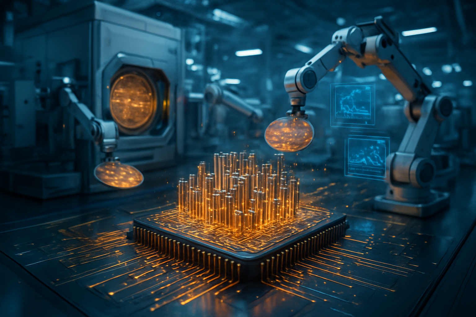
    The landscape of semiconductor technology for AI data centers is undergoing a profound transformation, driven by the escalating demands of artificial intelligence workloads. This evolution encompasses significant advancements in specialized AI accelerators, sophisticated packaging techniques, innovative memory solutions, and high-speed interconnects, each offering distinct technical specifications and representing a departure from previous approaches. The AI research community and industry experts are keenly observing and contributing to these developments, recognizing their critical role in scaling AI capabilities.

    Specialized AI accelerators are purpose-built hardware designed to expedite AI computations, such as neural network training and inference. Unlike traditional general-purpose GPUs, these accelerators are often tailored for specific AI tasks. Google's (NASDAQ: GOOGL) Tensor Processing Units (TPUs) are Application-Specific Integrated Circuits (ASICs) uniquely designed for deep learning workloads, especially within the TensorFlow framework, excelling in dense matrix operations fundamental to neural networks. TPUs employ systolic arrays, a computational architecture that minimizes memory fetches and control overhead, resulting in superior throughput and energy efficiency for their intended tasks. Google's Ironwood TPUs, for instance, have demonstrated nearly 30 times better energy efficiency than the first TPU generation. While TPUs offer specialized optimization, high-end GPUs like NVIDIA's (NASDAQ: NVDA) H100 and A100 remain prevalent in AI data centers due to their versatility and extensive ecosystem support for frameworks such as PyTorch, JAX, and TensorFlow. The NVIDIA H100 boasts up to 80 GB of high-bandwidth memory (HBM) and approximately 3.35 TB/s of bandwidth. The AI research community acknowledges TPUs' superior speed and energy efficiency for specific, large-scale, batch-heavy deep learning tasks using TensorFlow, but the flexibility and broader software support of GPUs make them a preferred choice for many researchers, particularly for experimental work.

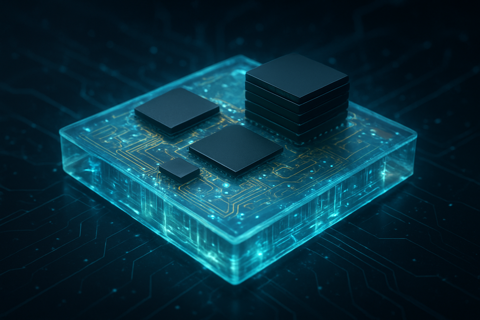
    As the physical limits of transistor scaling are approached, advanced packaging has become a critical driver for enhancing AI chip performance, power efficiency, and integration capabilities. 2.5D and 3D integration techniques revolutionize chip architectures: 2.5D packaging places multiple dies side-by-side on a passive silicon interposer, facilitating high-bandwidth communication, while 3D integration stacks active dies vertically, connecting them via Through-Silicon Vias (TSVs) for ultrafast signal transfer and reduced power consumption. NVIDIA's H100 GPUs use 2.5D integration to link logic and HBM. Chiplet architectures are smaller, modular dies integrated into a single package, offering unprecedented flexibility, scalability, and cost-efficiency. This allows for heterogeneous integration, combining different types of silicon (e.g., CPUs, GPUs, specialized accelerators, memory) into a single optimized package. AMD's (NASDAQ: AMD) MI300X AI accelerator, for example, integrates 3D SoIC and 2.5D CoWoS packaging. Industry experts like DIGITIMES chief semiconductor analyst Tony Huang emphasize that advanced packaging is now as critical as transistor scaling for system performance in the AI era, predicting a 45.5% compound annual growth rate for advanced packaging in AI data center chips from 2024 to 2030.

    The "memory wall"—where processor speed outpaces memory bandwidth—is a significant bottleneck for AI workloads. Novel memory solutions aim to overcome this by providing higher bandwidth, lower latency, and increased capacity. High Bandwidth Memory (HBM) is a 3D-stacked Synchronous Dynamic Random-Access Memory (SDRAM) that offers significantly higher bandwidth than traditional DDR4 or GDDR5. HBM3 provides bandwidth up to 819 GB/s per stack, and HBM4, with its specification finalized in April 2025, is expected to push bandwidth beyond 1 TB/s per stack and increase capacities. Compute Express Link (CXL) is an open, cache-coherent interconnect standard that enhances communication between CPUs, GPUs, memory, and other accelerators. CXL enables memory expansion beyond physical DIMM slots and allows memory to be pooled and shared dynamically across compute nodes, crucial for LLMs that demand massive memory capacities. The AI community views novel memory solutions as indispensable for overcoming the memory wall, with CXL heralded as a "game-changer" for AI and HPC.

    Efficient and high-speed communication between components is paramount for scaling AI data centers, as traditional interconnects are increasingly becoming bottlenecks for the massive data movement required. NVIDIA NVLink is a high-speed, point-to-point GPU interconnect that allows GPUs to communicate directly at much higher bandwidth and lower latency than PCIe. The fifth generation of NVLink provides up to 1.8 TB/s bidirectional bandwidth per GPU, more than double the previous generation. NVSwitch extends this capability by enabling all-to-all GPU communication across racks, forming a non-blocking compute fabric. Optical interconnects, leveraging silicon photonics, offer significantly higher bandwidth, lower latency, and reduced power consumption for both intra- and inter-data center communication. Companies like Ayar Labs are developing in-package optical I/O chiplets that deliver 2 Tbps per chiplet, achieving 1000x the bandwidth density and 10x faster latency and energy efficiency compared to electrical interconnects. Industry experts highlight that "data movement, not compute, is the largest energy drain" in modern AI data centers, consuming up to 60% of energy, underscoring the critical need for advanced interconnects.

    Reshaping the AI Battleground: Corporate Impact and Competitive Shifts

    The accelerating pace of semiconductor innovation for AI data centers is profoundly reshaping the landscape for AI companies, tech giants, and startups alike. This technological evolution is driven by the insatiable demand for computational power required by increasingly complex AI models, leading to a significant surge in demand for high-performance, energy-efficient, and specialized chips.

    A narrow set of companies with the scale, talent, and capital to serve hyperscale Cloud Service Providers (CSPs) are particularly well-positioned. GPU and AI accelerator manufacturers like NVIDIA (NASDAQ: NVDA) remain dominant, holding over 80% of the AI accelerator market, with AMD (NASDAQ: AMD) also a leader with its AI-focused server processors and accelerators. Intel (NASDAQ: INTC), while trailing some peers, is also developing AI ASICs. Memory manufacturers such as Micron Technology (NASDAQ: MU), Samsung Electronics (KRX: 005930), and SK Hynix (KRX: 000660) are major beneficiaries due to the exceptional demand for high-bandwidth memory (HBM). Foundries and packaging innovators like TSMC (NYSE: TSM), the world's largest foundry, are linchpins in the AI revolution, expanding production capacity. Cloud Service Providers (CSPs) and tech giants like Amazon (NASDAQ: AMZN) (AWS), Microsoft (NASDAQ: MSFT) (Azure), and Google (NASDAQ: GOOGL) (Google Cloud) are investing heavily in their own custom AI chips (e.g., Graviton, Trainium, Inferentia, Axion, Maia 100, Cobalt 100, TPUs) to optimize their cloud services and gain a competitive edge, reducing reliance on external suppliers.

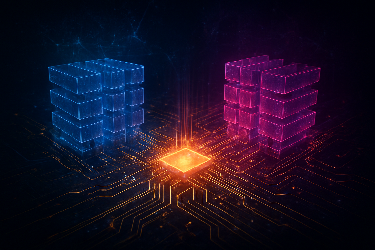
    The competitive landscape is becoming intensely dynamic. Tech giants and major AI labs are increasingly pursuing custom chip designs to reduce reliance on external suppliers and tailor hardware to their specific AI workloads, leading to greater control over performance, cost, and energy efficiency. Strategic partnerships are also crucial; for example, Anthropic's partnership with Microsoft and NVIDIA involves massive computing commitments and co-development efforts to optimize AI models for specific hardware architectures. This "compute-driven phase" creates higher barriers to entry for smaller AI labs that may struggle to match the colossal investments of larger firms. The need for specialized and efficient AI chips is also driving closer collaboration between hardware designers and AI developers, leading to holistic hardware-software co-design.

    These innovations are causing significant disruption. The dominance of traditional CPUs for AI workloads is being disrupted by specialized AI chips like GPUs, TPUs, NPUs, and ASICs, necessitating a re-evaluation of existing data center architectures. New memory technologies like HBM and CXL are disrupting traditional memory architectures. The massive power consumption of AI data centers is driving research into new semiconductor technologies that drastically reduce power usage, potentially by more than 1/100th of current levels, disrupting existing data center operational models. Furthermore, AI itself is disrupting the semiconductor design and manufacturing processes, with AI-driven chip design tools reducing design times and improving performance and power efficiency. Companies are gaining strategic advantages through specialization and customization, advanced packaging and integration, energy efficiency, ecosystem development, and leveraging AI within the semiconductor value chain.

    Beyond the Chip: Broader Implications for AI and Society

    The rapid evolution of Artificial Intelligence, particularly the emergence of large language models and deep learning, is fundamentally reshaping the semiconductor industry. This symbiotic relationship sees AI driving an unprecedented demand for specialized hardware, while advancements in semiconductor technology, in turn, enable more powerful and efficient AI systems. These innovations are critical for the continued growth and scalability of AI data centers, but they also bring significant challenges and wider implications across the technological, economic, and geopolitical landscapes.

    These innovations are not just about faster chips; they represent a fundamental shift in how AI computation is approached, moving towards increased specialization, hybrid architectures combining different processors, and a blurring of the lines between edge and cloud computing. They enable the training and deployment of increasingly complex and capable AI models, including multimodal generative AI and agentic AI, which can autonomously plan and execute multi-step workflows. Specialized chips offer superior performance per watt, crucial for managing the growing computational demands, with NVIDIA's accelerated computing, for example, being up to 20 times more energy efficient than traditional CPU-only systems for AI tasks. This drives a new "semiconductor supercycle," with the global AI hardware market projected for significant growth and companies focused on AI chips experiencing substantial valuation surges.

    Despite the transformative potential, these innovations raise several concerns. The exponential growth of AI workloads in data centers is leading to a significant surge in power consumption and carbon emissions. AI servers consume 7 to 8 times more power than general CPU-based servers, with global data center electricity consumption projected to nearly double by 2030. This increased demand is outstripping the rate at which new electricity is being added to grids, raising urgent questions about sustainability, cost, and infrastructure capacity. The production of advanced AI chips is concentrated among a few key players and regions, particularly in Asia, making advanced semiconductors a focal point of geopolitical tensions and potentially impacting supply chains and accessibility. The high cost of advanced AI chips also poses an accessibility challenge for smaller organizations.

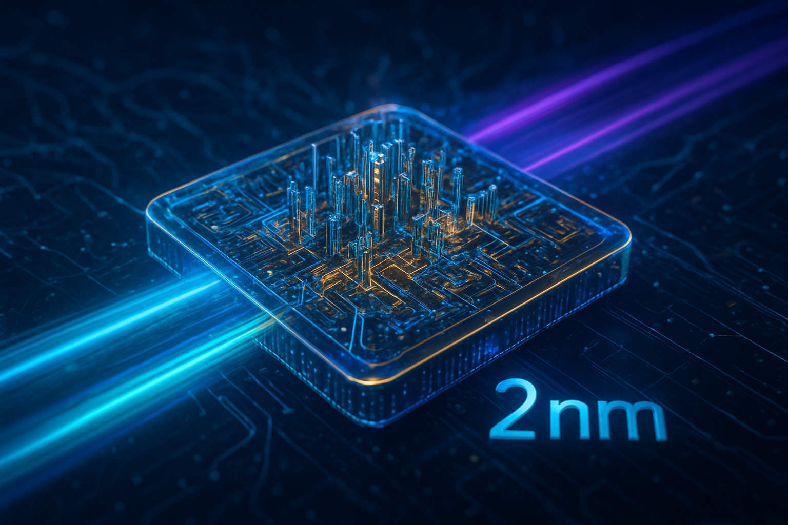
    The current wave of semiconductor innovation for AI data centers can be compared to several previous milestones in computing. It echoes the transistor revolution and integrated circuits that replaced bulky vacuum tubes, laying the foundational hardware for all subsequent computing. It also mirrors the rise of microprocessors that ushered in the personal computing era, democratizing computing power. While Moore's Law, which predicted the doubling of transistors, guided advancements for decades, current innovations, driven by AI's demands for specialized hardware (GPUs, ASICs, neuromorphic chips) rather than just general-purpose scaling, represent a new paradigm. This signifies a shift from simply packing more transistors to designing architectures specifically optimized for AI workloads, much like the resurgence of neural networks shifted computational demands towards parallel processing.

    The Road Ahead: Anticipating AI Semiconductor's Next Frontiers

    Future developments in AI semiconductor innovation for data centers are characterized by a relentless pursuit of higher performance, greater energy efficiency, and specialized architectures to support the escalating demands of artificial intelligence workloads. The market for AI chips in data centers is projected to reach over $400 billion by 2030, highlighting the significant growth expected in this sector.

    In the near term, the AI semiconductor landscape will continue to be dominated by GPUs for AI training, with companies like NVIDIA (NASDAQ: NVDA), AMD (NASDAQ: AMD), and Intel (NASDAQ: INTC) leading the way. There is also a significant rise in the development and adoption of custom AI Application-Specific Integrated Circuits (ASICs) by hyperscalers such as Google (NASDAQ: GOOGL), Amazon (NASDAQ: AMZN), and Microsoft (NASDAQ: MSFT). Memory innovation is critical, with increasing adoption of DDR5 and High Bandwidth Memory (HBM) for AI training, and Compute Express Link (CXL) gaining traction to address memory disaggregation and latency issues. Advanced packaging technologies, such as 2.5D and 3D stacking, are becoming crucial for integrating diverse components for improved performance. Long-term, the focus will intensify on even more energy-efficient designs and novel architectures, aiming to reduce power consumption by over 100 times compared to current levels. The concept of "accelerated computing," combining GPUs with CPUs, is expected to become the dominant path forward, significantly more energy-efficient than traditional CPU-only systems for AI tasks.

    These advancements will enable a wide array of sophisticated applications. Generative AI and Large Language Models (LLMs) will be at the forefront, used for content generation, query answering, and powering advanced virtual assistants. AI chips will continue to fuel High-Performance Computing (HPC) across scientific and industrial domains. Industrial automation, real-time decision-making, drug discovery, and autonomous infrastructure will all benefit. Edge AI integration, allowing for real-time responses and better security in applications like self-driving cars and smart glasses, will also be significantly impacted. However, several challenges need to be addressed, including power consumption and thermal management, supply chain constraints and geopolitical tensions, massive capital expenditure for infrastructure, and the difficulty of predicting demand in rapidly innovating cycles.

    Experts predict a dramatic acceleration in AI technology adoption. NVIDIA's CEO, Jensen Huang, believes that large language models will become ubiquitous, and accelerated computing will be the future of data centers due to its efficiency. The total semiconductor market for data centers is expected to grow significantly, with GPUs projected to more than double their revenue, and AI ASICs expected to skyrocket. There is a consensus on the urgent need for integrated solutions to address the power consumption and environmental impact of AI data centers, including more efficient semiconductor designs, AI-optimized software for energy management, and the adoption of renewable energy sources. However, concerns remain about whether global semiconductor chip manufacturing capacity can keep pace with projected demand, and if power availability and data center construction speed will become the new limiting factors for AI infrastructure expansion.

    Charting the Course: A New Era for AI Infrastructure

    The landscape of semiconductor innovation for next-generation AI data centers is undergoing a profound transformation, driven by the insatiable demand for computational power, efficiency, and scalability required by advanced AI models, particularly generative AI. This shift is reshaping chip design, memory architectures, data center infrastructure, and the competitive dynamics of the semiconductor industry.

    Key takeaways include the explosive growth in AI chip performance, with GPUs leading the charge and mid-generation refreshes boosting memory bandwidth. Advanced memory technologies like HBM and CXL are indispensable, addressing memory bottlenecks and enabling disaggregated memory architectures. The shift towards chiplet architectures is overcoming the physical and economic limits of monolithic designs, offering modularity, improved yields, and heterogeneous integration. The rise of Domain-Specific Architectures (DSAs) and ASICs by hyperscalers signifies a strategic move towards highly specialized hardware for optimized performance and reduced dependence on external vendors. Crucial infrastructure innovations in cooling and power delivery, including liquid cooling and power delivery chiplets, are essential to manage the unprecedented power density and heat generation of AI chips, with sustainability becoming a central driving force.

    These semiconductor innovations represent a pivotal moment in AI history, a "structural shift" enabling the current generative AI revolution and fundamentally reshaping the future of computing. They are enabling the training and deployment of increasingly complex AI models that would be unattainable without these hardware breakthroughs. Moving beyond the conventional dictates of Moore's Law, chiplet architectures and domain-specific designs are providing new pathways for performance scaling and efficiency. While NVIDIA (NASDAQ: NVDA) currently holds a dominant position, the rise of ASICs and chiplets fosters a more open and multi-vendor future for AI hardware, potentially leading to a democratization of AI hardware. Moreover, AI itself is increasingly used in chip design and manufacturing processes, accelerating innovation and optimizing production.

    The long-term impact will be profound, transforming data centers into "AI factories" specialized in continuously creating intelligence at an industrial scale, redefining infrastructure and operational models. This will drive massive economic transformation, with AI projected to add trillions to the global economy. However, the escalating energy demands of AI pose a significant sustainability challenge, necessitating continued innovation in energy-efficient chips, cooling systems, and renewable energy integration. The global semiconductor supply chain will continue to reconfigure, influenced by strategic investments and geopolitical factors. The trend toward continued specialization and heterogeneous computing through chiplets will necessitate advanced packaging and robust interconnects.

    In the coming weeks and months, watch for further announcements and deployments of next-generation HBM (HBM4 and beyond) and wider adoption of CXL to address memory bottlenecks. Expect accelerated chiplet adoption by major players in their next-generation GPUs (e.g., Rubin GPUs in 2026), alongside the continued rise of AI ASICs and custom silicon from hyperscalers, intensifying competition. Rapid advancements and broader implementation of liquid cooling solutions and innovative power delivery mechanisms within data centers will be critical. The focus on interconnects and networking will intensify, with innovations in network fabrics and silicon photonics crucial for large-scale AI training clusters. Finally, expect growing emphasis on sustainable AI hardware and data center operations, including research into energy-efficient chip architectures and increased integration of renewable energy sources.


    This content is intended for informational purposes only and represents analysis of current AI developments.

    TokenRing AI delivers enterprise-grade solutions for multi-agent AI workflow orchestration, AI-powered development tools, and seamless remote collaboration platforms.
    For more information, visit https://www.tokenring.ai/.

  • The Brain-Inspired Revolution: Neuromorphic Architectures Propel AI Beyond the Horizon

    The Brain-Inspired Revolution: Neuromorphic Architectures Propel AI Beyond the Horizon

    In a groundbreaking era of artificial intelligence, a revolutionary computing paradigm known as neuromorphic computing is rapidly gaining prominence, promising to redefine the very foundations of how machines learn, process information, and interact with the world. Drawing profound inspiration from the human brain's intricate structure and functionality, this technology is moving far beyond its initial applications in self-driving cars, poised to unlock unprecedented levels of energy efficiency, real-time adaptability, and cognitive capabilities across a vast spectrum of industries. As the conventional Von Neumann architecture increasingly strains under the demands of modern AI, neuromorphic computing emerges as a pivotal solution, heralding a future of smarter, more sustainable, and truly intelligent machines.

    Technical Leaps: Unpacking the Brain-Inspired Hardware and Software

    Neuromorphic architectures represent a radical departure from traditional computing, fundamentally rethinking how processing and memory interact. Unlike the Von Neumann architecture, which separates the CPU and memory, leading to the infamous "Von Neumann bottleneck," neuromorphic chips integrate these functions directly within artificial neurons and synapses. This allows for massively parallel, event-driven processing, mirroring the brain's efficient communication through discrete electrical "spikes."

    Leading the charge in hardware innovation are several key players. Intel (NASDAQ: INTC) has been a significant force with its Loihi series. The original Loihi chip, introduced in 2017, demonstrated a thousand-fold improvement in efficiency for certain neural networks. Its successor, Loihi 2 (released in 2021), advanced with 1 million artificial neurons and 120 million synapses, optimizing for scale, speed, and efficiency using spiking neural networks (SNNs). Most notably, in 2024, Intel unveiled Hala Point, the world's largest neuromorphic system, boasting an astounding 1.15 billion neurons and 128 billion synapses across 1,152 Loihi 2 processors. Deployed at Sandia National Laboratories, Hala Point is showcasing significant efficiency gains for robotics, healthcare, and IoT applications, processing signals 20 times faster than a human brain for some tasks.

    IBM (NYSE: IBM) has also made substantial contributions with its TrueNorth chip, an early neuromorphic processor accommodating 1 million programmable neurons and 256 million synapses with remarkable energy efficiency (70 milliwatts). In 2023, IBM introduced NorthPole, a chip designed for highly efficient artificial neural network inference, claiming 25 times more energy efficiency and 22 times faster performance than NVIDIA's V100 GPU for specific inference tasks.

    Other notable hardware innovators include BrainChip (ASX: BRN) with its Akida neuromorphic processor, an ultra-low-power, event-driven chip optimized for edge AI inference and learning. The University of Manchester's SpiNNaker (Spiking Neural Network Architecture) and its successor SpiNNaker 2 are million-core supercomputers designed to simulate billions of neurons. Heidelberg University's BrainScaleS-2 and Stanford University's Neurogrid also contribute to the diverse landscape of neuromorphic hardware. Startups like SynSense and Innatera are developing ultra-low-power, event-driven processors for real-time AI. Furthermore, advancements extend to event-based sensors, such as Prophesee's Metavision, which only activate upon detecting changes, leading to high temporal resolution and extreme energy efficiency.

    Software innovations are equally critical, albeit still maturing. The core computational model is the Spiking Neural Network (SNN), which encodes information in the timing and frequency of spikes, drastically reducing computational overhead. New training paradigms are emerging, as traditional backpropagation doesn't directly translate to spike-based systems. Open-source frameworks like BindsNET, Norse, Rockpool, snnTorch, Spyx, and SpikingJelly are facilitating SNN simulation and training, often leveraging existing deep learning infrastructures like PyTorch.

    The AI research community and industry experts have expressed "overwhelming positivity" towards neuromorphic computing, viewing it as a "breakthrough year" as the technology transitions from academia to tangible commercial products. While optimism abounds regarding its energy efficiency and real-time AI capabilities, challenges remain, including immature software ecosystems, the need for standardized tools, and proving a clear value proposition against established GPU solutions for mainstream applications. Some current neuromorphic processors still face latency and scalability issues, leading to a debate on whether they will remain niche or become a mainstream alternative, particularly for the "extreme edge" segment.

    Corporate Chessboard: Beneficiaries, Disruptors, and Strategic Plays

    Neuromorphic computing is poised to fundamentally reshape the competitive landscape for AI companies, tech giants, and startups, creating a new arena for innovation and strategic advantage. Its inherent benefits in energy efficiency, real-time processing, and adaptive learning are driving a strategic pivot across the industry.

    Tech giants are heavily invested in neuromorphic computing, viewing it as a critical area for future AI leadership. Intel (NASDAQ: INTC), through its Intel Neuromorphic Research Community (INRC) and the recent launch of Hala Point, is positioning itself as a leader in large-scale neuromorphic systems. These efforts are not just about research; they aim to deliver significant efficiency gains for demanding AI applications in robotics, healthcare, and IoT, potentially reducing power consumption by orders of magnitude compared to traditional processors. IBM (NYSE: IBM) continues its pioneering work with TrueNorth and NorthPole, focusing on developing highly efficient AI inference engines that push the boundaries of performance per watt. Qualcomm (NASDAQ: QCOM) is developing its Zeroth platform, a brain-inspired computing architecture for mobile devices, robotics, and wearables, aiming to enable advanced AI operations directly on the device, reducing cloud dependency and enhancing privacy. Samsung is also heavily invested, exploring specialized processors and integrated memory solutions. These companies are engaged in a competitive race to develop neuromorphic chips with specialized architectures, focusing on energy efficiency, real-time learning, and robust hardware-software co-design for a new generation of AI applications.

    Startups are finding fertile ground in this emerging field, often focusing on niche market opportunities. BrainChip (ASX: BRN) is a pioneer with its Akida neuromorphic processor, targeting ultra-low-power edge AI inference and learning, especially for smart cameras and IoT devices. GrAI Matter Labs develops brain-inspired AI processors for edge applications, emphasizing ultra-low latency for machine vision in robotics and AR/VR. Innatera Nanosystems specializes in ultra-low-power analog neuromorphic processors for advanced cognitive applications, while SynSense focuses on neuromorphic sensing and computing solutions for real-time AI. Other innovative startups include MemComputing, Rain.AI, Opteran, Aspirare Semi, Vivum Computing, and General Vision Inc., all aiming to disrupt the market with unique approaches to brain-inspired computing.

    The competitive implications are profound. Neuromorphic computing is emerging as a disruptive force to the traditional GPU-dominated AI hardware market. While GPUs from companies like NVIDIA (NASDAQ: NVDA) are powerful, their energy intensity is a growing concern. The rise of neuromorphic computing could prompt these tech giants to strategically pivot towards specialized AI silicon or acquire neuromorphic expertise. Companies that successfully integrate neuromorphic computing stand to gain significant strategic advantages through superior energy efficiency, real-time decision-making, enhanced data privacy and security (due to on-chip learning), and inherent robustness. However, challenges remain, including the current decreased accuracy when converting deep neural networks to spiking neural networks, a lack of benchmarks, limited accessibility, and emerging cybersecurity threats like neuromorphic mimicry attacks (NMAs).

    A Broader Canvas: AI Landscape, Ethics, and Historical Echoes

    Neuromorphic computing represents more than just an incremental improvement; it's a fundamental paradigm shift that is reshaping the broader AI landscape. By moving beyond the traditional Von Neumann architecture, which separates processing and memory, neuromorphic systems inherently address the "Von Neumann bottleneck," a critical limitation for modern AI workloads. This brain-inspired design, utilizing artificial neurons and synapses that communicate via "spikes," promises unprecedented energy efficiency, processing speed, and real-time adaptability—qualities that are increasingly vital as AI models grow in complexity and computational demand.

    Its alignment with current AI trends is clear. As deep learning models become increasingly energy-intensive, neuromorphic computing offers a sustainable path forward, potentially reducing power consumption by orders of magnitude. This efficiency is crucial for the widespread deployment of AI in power-constrained edge devices and for mitigating the environmental impact of large-scale AI computations. Furthermore, its ability for on-chip, real-time learning and adaptation directly addresses the limitations of traditional AI, which often requires extensive offline retraining on massive, labeled datasets.

    However, this transformative technology also brings significant societal and ethical considerations. The ability of neuromorphic systems to learn and make autonomous decisions raises critical questions about accountability, particularly in applications like autonomous vehicles and environmental management. Like traditional AI, neuromorphic systems are susceptible to algorithmic bias if trained on flawed data, necessitating robust frameworks for explainability and transparency. Privacy and security are paramount, as these systems will process vast amounts of data, making compliance with data protection regulations crucial. The complex nature of neuromorphic chips also introduces new vulnerabilities, requiring advanced defense mechanisms against potential breaches and novel attack vectors. On a deeper philosophical level, the development of machines that can mimic human cognitive functions so closely prompts profound questions about human-machine interaction, consciousness, and even the legal status of highly advanced AI.

    Compared to previous AI milestones, neuromorphic computing stands out as a foundational infrastructural shift. While breakthroughs in deep learning and specialized AI accelerators transformed the field by enabling powerful pattern recognition, neuromorphic computing offers a new computational substrate. It moves beyond the energy crisis of current AI by providing significantly higher energy efficiency and enables real-time, adaptive learning with smaller datasets—a capability vital for autonomous and personalized AI that continuously learns and evolves. This shift is akin to the advent of specialized AI accelerators, providing a new hardware foundation upon which the next generation of algorithmic breakthroughs can be built, pushing the boundaries of what machines can learn and achieve.

    The Horizon: Future Trajectories and Expert Predictions

    The future of neuromorphic computing is brimming with potential, with both near-term and long-term advancements poised to revolutionize artificial intelligence and computation. Experts anticipate a rapid evolution, driven by continued innovation in hardware, software, and a growing understanding of biological intelligence.

    In the near term (1-5 years, extending to 2030), the most prominent development will be the widespread proliferation of neuromorphic chips in edge AI and Internet of Things (IoT) devices. This includes smart home systems, drones, robots, and various sensors, enabling localized, real-time data processing with enhanced AI capabilities, crucial for resource-constrained environments. Hardware will continue to improve with cutting-edge materials and architectures, including the integration of memristive devices that mimic synaptic connections for even lower power consumption. The development of spintronic devices is also expected to contribute to significant power reduction and faster switching speeds, potentially enabling truly neuromorphic AI hardware by 2030.

    Looking further into the long term (beyond 2030), the vision for neuromorphic computing includes achieving truly cognitive AI and potentially Artificial General Intelligence (AGI). This promises more efficient learning, real-time adaptation, and robust information processing that closely mirrors human cognitive functions. Experts predict the emergence of hybrid computing systems, seamlessly combining traditional CPU/GPU cores with neuromorphic processors to leverage the strengths of each. Novel materials beyond silicon, such as graphene and carbon nanotubes, coupled with 3D integration and nanotechnology, will allow for denser component integration, enhancing performance and energy efficiency. The refinement of advanced learning algorithms inspired by neuroscience, including unsupervised, reinforcement, and continual learning, will be a major focus.

    Potential applications on the horizon are vast, spanning across multiple sectors. Beyond autonomous systems and robotics, neuromorphic computing will enhance AI systems for machine learning and cognitive computing tasks, especially where energy-efficient processing is critical. It will revolutionize sensory processing for smart cameras, traffic management, and advanced voice recognition. In cybersecurity, it will enable advanced threat detection and anomaly recognition due to its rapid pattern identification capabilities. Healthcare stands to benefit significantly from real-time data processing for wearable health monitors, intelligent prosthetics, and even brain-computer interfaces (BCI). Scientific research will also be advanced through more efficient modeling and simulation in fields like neuroscience and epidemiology.

    Despite this immense promise, several challenges need to be addressed. The lack of standardized benchmarks and a mature software ecosystem remains a significant hurdle. Developing algorithms that accurately mimic intricate neural processes and efficiently train spiking neural networks is complex. Hardware scalability, integration with existing systems, and manufacturing variations also pose technical challenges. Furthermore, current neuromorphic systems may not always match the accuracy of traditional computers for certain tasks, and the interdisciplinary nature of the field requires extensive collaboration across bioscience, mathematics, neuroscience, and computer science.

    However, experts are overwhelmingly optimistic. The neuromorphic computing market is projected for substantial growth, with estimates suggesting it will reach USD 54.05 billion by 2035, driven by the demand for higher-performing integrated circuits and the increasing need for AI and machine learning. Many believe neuromorphic computing will revolutionize AI by enabling algorithms to run at the edge, addressing the anticipated end of Moore's Law, and significantly reducing the escalating energy demands of current AI models. The next wave of AI is expected to be a "marriage of physics and neuroscience," with neuromorphic chips leading the way to more human-like intelligence.

    A New Era of Intelligence: The Road Ahead

    Neuromorphic computing stands as a pivotal development in the annals of AI history, representing not merely an evolution but a fundamental re-imagination of computational architecture. Its core principle—mimicking the human brain's integrated processing and memory—offers a compelling solution to the "Von Neumann bottleneck" and the escalating energy demands of modern AI. By prioritizing energy efficiency, real-time adaptability, and on-chip learning through spiking neural networks, neuromorphic systems promise to usher in a new era of intelligent machines that are inherently more sustainable, responsive, and capable of operating autonomously in complex, dynamic environments.

    The significance of this development cannot be overstated. It provides a new computational substrate that can enable the next generation of algorithmic breakthroughs, pushing the boundaries of what machines can learn and achieve. While challenges persist in terms of software ecosystems, standardization, and achieving universal accuracy, the industry is witnessing a critical inflection point as neuromorphic computing transitions from promising research to tangible commercial products.

    In the coming weeks and months, the tech world will be watching for several key developments. Expect further commercialization and product rollouts from major players like Intel (NASDAQ: INTC) with its Loihi series and BrainChip (ASX: BRN) with its Akida processor, alongside innovative startups like Innatera. Increased funding and investment in neuromorphic startups will signal growing confidence in the market. Key milestones anticipated for 2026 include the establishment of standardized neuromorphic benchmarks through IEEE P2800, mass production of neuromorphic microcontrollers, and the potential approval of the first medical devices powered by this technology. The integration of neuromorphic edge AI into consumer electronics, IoT, and lifestyle devices, possibly showcased at events like CES 2026, will mark a significant step towards mainstream adoption. Continued advancements in materials, architectures, and user-friendly software development tools will be crucial for wider acceptance. Furthermore, strategic partnerships between academia and industry, alongside growing industry adoption in niche verticals like cybersecurity, event-based vision, and autonomous robotics, will underscore the technology's growing impact. The exploration by companies like Mercedes-Benz (FWB: MBG) into BrainChip's Akida for in-vehicle AI highlights the tangible interest from major industries.

    Neuromorphic computing is not just a technological advancement; it's a philosophical leap towards building AI that more closely resembles biological intelligence. As we move closer to replicating the brain's incredible efficiency and adaptability, the long-term impact on healthcare, autonomous systems, edge computing, and even our understanding of intelligence itself will be profound. The journey from silicon to synthetic consciousness is long, but neuromorphic architectures are undoubtedly paving a fascinating and critical path forward.


    This content is intended for informational purposes only and represents analysis of current AI developments.

    TokenRing AI delivers enterprise-grade solutions for multi-agent AI workflow orchestration, AI-powered development tools, and seamless remote collaboration platforms.
    For more information, visit https://www.tokenring.ai/.