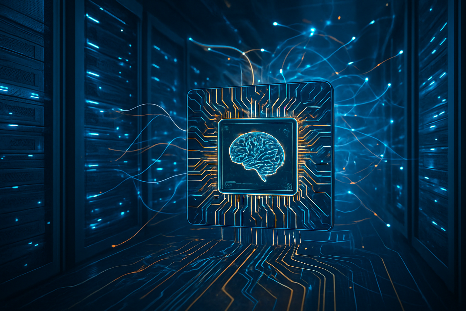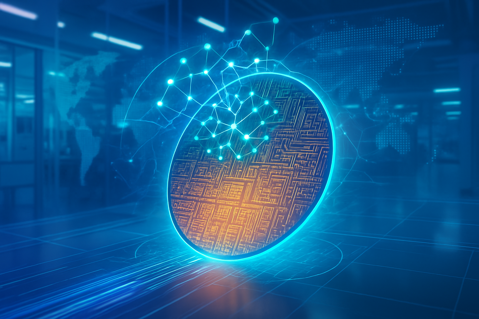
The relentless march of artificial intelligence (AI) is not solely a triumph of algorithms and data; it is fundamentally underpinned and accelerated by profound advancements in semiconductor technology. From the foundational logic gates of the 20th century to today's highly specialized AI accelerators, silicon has evolved to become the indispensable backbone of every AI breakthrough. This symbiotic relationship sees AI's insatiable demand for computational power driving unprecedented innovation in chip design and manufacturing, while these cutting-edge chips, in turn, unlock previously unimaginable AI capabilities, propelling us into an era of pervasive intelligence.
This deep dive explores how specialized semiconductor architectures are not just supporting, but actively enabling and reshaping the AI landscape, influencing everything from cloud-scale training of massive language models to real-time inference on tiny edge devices. The ongoing revolution in silicon is setting the pace for AI's evolution, dictating what is computationally possible, economically viable, and ultimately, how quickly AI transforms industries and daily life.
Detailed Technical Coverage: The Engines of AI
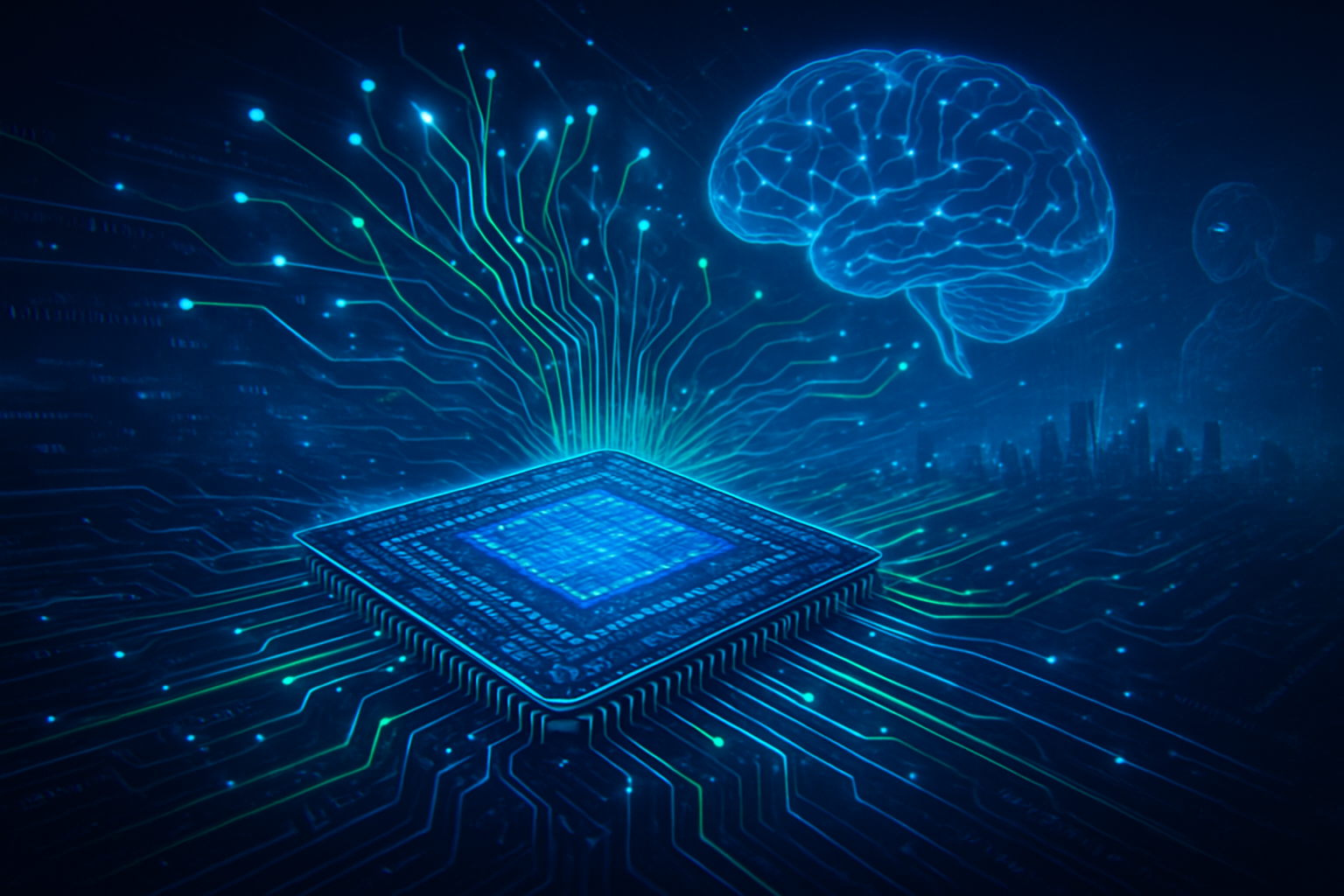
The journey of AI from theoretical concept to practical reality has been inextricably linked to the evolution of processing hardware. Initially, general-purpose Central Processing Units (CPUs) handled AI tasks, but their sequential processing architecture proved inefficient for the massively parallel computations inherent in neural networks. This limitation spurred the development of specialized semiconductor technologies designed to accelerate AI workloads, leading to significant performance gains and opening new frontiers for AI research and application.
Graphics Processing Units (GPUs) emerged as the first major accelerator for AI. Originally designed for rendering complex graphics, GPUs feature thousands of smaller, simpler cores optimized for parallel processing. Companies like NVIDIA (NASDAQ: NVDA) have been at the forefront, introducing innovations like Tensor Cores in their Volta architecture (2017) and subsequent generations (e.g., H100, Blackwell), which are specialized units for rapid matrix multiply-accumulate operations fundamental to deep learning. These GPUs, supported by comprehensive software platforms like CUDA, can train complex neural networks in hours or days, a task that would take weeks on traditional CPUs, fundamentally transforming deep learning from an academic curiosity into a production-ready discipline.
Beyond GPUs, Application-Specific Integrated Circuits (ASICs) like Google's Tensor Processing Units (TPUs) represent an even more specialized approach. Introduced in 2016, TPUs are custom-built ASICs specifically engineered to accelerate TensorFlow operations, utilizing a unique systolic array architecture. This design streams data through a matrix of multiply-accumulators, minimizing memory fetches and achieving exceptional efficiency for dense matrix multiplications—the core operation in neural networks. While sacrificing flexibility compared to GPUs, TPUs offer superior speed and power efficiency for specific AI workloads, particularly in large-scale model training and inference within Google's cloud ecosystem. The latest generations, such as Ironwood, promise even greater performance and energy efficiency, attracting major AI labs like Anthropic, which plans to leverage millions of these chips.
Field-Programmable Gate Arrays (FPGAs) offer a middle ground between general-purpose processors and fixed-function ASICs. FPGAs are reconfigurable chips whose hardware logic can be reprogrammed after manufacturing, allowing for the implementation of custom hardware architectures directly onto the chip. This flexibility enables fine-grained optimization for specific AI algorithms, delivering superior power efficiency and lower latency for tailored workloads, especially in edge AI applications where real-time processing and power constraints are critical. While their development complexity can be higher, FPGAs provide adaptability to evolving AI models without the need for new silicon fabrication. Finally, neuromorphic chips, like Intel's Loihi and IBM's TrueNorth, represent a radical departure, mimicking the human brain's structure and event-driven processing. These chips integrate memory and processing, utilize spiking neural networks, and aim for ultra-low power consumption and on-chip learning, holding immense promise for truly energy-efficient and adaptive AI, particularly for edge devices and continuous learning scenarios.
Competitive Landscape: Who Benefits and Why
The advanced semiconductor landscape is a fiercely contested arena, with established giants and innovative startups vying for supremacy in the AI era. The insatiable demand for AI processing power has reshaped competitive dynamics, driven massive investments, and fostered a significant trend towards vertical integration.
NVIDIA (NASDAQ: NVDA) stands as the undisputed market leader, capturing an estimated 80-85% of the AI chip market. Its dominance stems not only from its powerful GPUs (like the A100 and H100) but also from its comprehensive CUDA software ecosystem, which has fostered a vast developer community and created significant vendor lock-in. NVIDIA's strategy extends to offering full "AI Factories"—integrated, rack-scale systems—further solidifying its indispensable role in AI infrastructure. Intel (NASDAQ: INTC) is repositioning itself with its Xeon Scalable processors, specialized Gaudi AI accelerators, and a renewed focus on manufacturing leadership with advanced nodes like 18A. However, Intel faces the challenge of building out its software ecosystem to rival CUDA. AMD (NASDAQ: AMD) is aggressively challenging NVIDIA with its MI300 series (MI300X, MI355, MI400), offering competitive performance and pricing, alongside an open-source ROCm ecosystem to attract enterprises seeking alternatives to NVIDIA's proprietary solutions.
Crucially, Taiwan Semiconductor Manufacturing Company (TSMC) (NYSE: TSM) remains an indispensable architect of the AI revolution, acting as the primary foundry for nearly all cutting-edge AI chips from NVIDIA, Apple (NASDAQ: AAPL), AMD, Amazon (NASDAQ: AMZN), and Google (NASDAQ: GOOGL). TSMC's technological leadership in advanced process nodes (e.g., 3nm, 2nm) and packaging solutions (e.g., CoWoS) is critical for the performance and power efficiency demanded by advanced AI processors, making it a linchpin in the global AI supply chain. Meanwhile, major tech giants and hyperscalers—Google, Microsoft (NASDAQ: MSFT), and Amazon Web Services (AWS)—are heavily investing in designing their own custom AI chips (ASICs) like Google's TPUs, Microsoft's Maia and Cobalt, and AWS's Trainium and Inferentia. This vertical integration strategy aims to reduce reliance on third-party vendors, optimize performance for their specific cloud AI workloads, control escalating costs, and enhance energy efficiency, potentially disrupting the market for general-purpose AI accelerators.
The rise of advanced semiconductors is also fostering innovation among AI startups. Companies like Celestial AI (optical interconnects), SiMa.ai (edge AI), Enfabrica (ultra-fast connectivity), Hailo (generative AI at the edge), and Groq (inference-optimized Language Processing Units) are carving out niches by addressing specific bottlenecks or offering specialized solutions that push the boundaries of performance, power efficiency, or cost-effectiveness beyond what general-purpose chips can achieve. This dynamic environment ensures continuous innovation, challenging established players and driving the industry forward.
Broader Implications: Shaping Society and the Future
The pervasive integration of advanced semiconductor technology into AI systems carries profound wider significance, shaping not only the technological landscape but also societal structures, economic dynamics, and geopolitical relations. This technological synergy is driving a new era of AI, distinct from previous cycles.
The impact on AI development and deployment is transformative. Specialized AI chips are essential for enabling increasingly complex AI models, particularly large language models (LLMs) and generative AI, which demand unprecedented computational power to process vast datasets. This hardware acceleration has been a key factor in the current "AI boom," moving AI from limited applications to widespread deployment across industries like healthcare, automotive, finance, and manufacturing. Furthermore, the push for Edge AI, where processing occurs directly on devices, is making AI ubiquitous, enabling real-time applications in autonomous systems, IoT, and augmented reality, reducing latency, enhancing privacy, and conserving bandwidth. Interestingly, AI is also becoming a catalyst for semiconductor innovation itself, with AI algorithms optimizing chip design, automating verification, and improving manufacturing processes, creating a self-reinforcing cycle of progress.
However, this rapid advancement is not without concerns. Energy consumption stands out as a critical issue. AI data centers are already consuming a significant and rapidly growing portion of global electricity, with high-performance AI chips being notoriously power-hungry. This escalating energy demand contributes to a substantial environmental footprint, necessitating a strong focus on energy-efficient chip designs, advanced cooling solutions, and sustainable data center operations. Geopolitical implications are equally pressing. The highly concentrated nature of advanced semiconductor manufacturing, primarily in Taiwan and South Korea, creates supply chain vulnerabilities and makes AI chips a flashpoint in international relations, particularly between the United States and China. Export controls and tariffs underscore a global "tech race" for technological supremacy, impacting global AI development and national security.
Comparing this era to previous AI milestones reveals a fundamental difference: hardware is now a critical differentiator. Unlike past "AI winters" where computational limitations hampered progress, the availability of specialized, high-performance semiconductors has been the primary enabler of the current AI boom. This shift has led to faster adoption rates and deeper market disruption than ever before, moving AI from experimental to practical and pervasive. The "AI on Edge" movement further signifies a maturation, bringing real-time, local processing to everyday devices and marking a pivotal transition from theoretical capability to widespread integration into society.
The Road Ahead: Future Horizons in AI Semiconductors
The trajectory of AI semiconductor development points towards a future characterized by continuous innovation, novel architectures, and a relentless pursuit of both performance and efficiency. Experts predict a dynamic landscape where current trends intensify and revolutionary paradigms begin to take shape.
In the near-term (1-3 years), we can expect further advancements in advanced packaging technologies, such as 3D stacking and heterogeneous integration, which will overcome traditional 2D scaling limits by allowing more transistors and diverse components to be packed into smaller, more efficient packages. The transition to even smaller process nodes, like 3nm and 2nm, enabled by cutting-edge High-NA EUV lithography, will continue to deliver higher transistor density, boosting performance and power efficiency. Specialized AI chip architectures will become even more refined, with new generations of GPUs from NVIDIA and AMD, and custom ASICs from hyperscalers, tailored for specific AI workloads like large language model deployment or real-time edge inference. The evolution of High Bandwidth Memory (HBM), with HBM3e and the forthcoming HBM4, will remain crucial for alleviating memory bottlenecks that plague data-intensive AI models. The proliferation of Edge AI capabilities will also accelerate, with AI PCs featuring integrated Neural Processing Units (NPUs) becoming standard, and more powerful, energy-efficient chips enabling sophisticated AI in autonomous systems and IoT devices.
Looking further ahead (beyond 3 years), truly transformative technologies are on the horizon. Neuromorphic computing, which mimics the brain's spiking neural networks and in-memory processing, promises unparalleled energy efficiency for adaptive, real-time learning on constrained devices. While still in its early stages, quantum computing holds the potential to revolutionize AI by solving optimization and cryptography problems currently intractable for classical computers, drastically reducing training times for certain models. Silicon photonics, integrating optical and electronic components, could address interconnect latency and power consumption by using light for data transmission. Research into new materials beyond silicon (e.g., 2D materials like graphene) and novel transistor designs (e.g., Gate-All-Around) will continue to push the fundamental limits of chip performance. Experts also predict the emergence of "codable" hardware that can dynamically adapt to evolving AI requirements, allowing chips to be reconfigured more flexibly for future AI models and algorithms.
However, significant challenges persist. The physical limits of scaling (beyond Moore's Law), including atomic-level precision, quantum tunneling, and heat dissipation, demand innovative solutions. The explosive power consumption of AI, particularly for training large models, necessitates a continued focus on energy-efficient designs and advanced cooling. Software complexity and the need for seamless hardware-software co-design remain critical, as optimizing AI algorithms for diverse hardware architectures is a non-trivial task. Furthermore, supply chain resilience in a geopolitically charged environment and a persistent talent shortage in semiconductor and AI fields must be addressed to sustain this rapid pace of innovation.
Conclusion: The Unfolding Chapter of AI and Silicon
The narrative of artificial intelligence in the 21st century is fundamentally intertwined with the story of semiconductor advancement. From the foundational role of GPUs in enabling deep learning to the specialized architectures of ASICs and the futuristic promise of neuromorphic computing, silicon has proven to be the indispensable engine powering the AI revolution. This symbiotic relationship, where AI drives chip innovation and chips unlock new AI capabilities, is not just a technological trend but a defining force shaping our digital future.
The significance of this development in AI history cannot be overstated. We are witnessing a pivotal transformation where AI has moved from theoretical possibility to pervasive reality, largely thanks to the computational muscle provided by advanced semiconductors. This era marks a departure from previous AI cycles, with hardware now a critical differentiator, enabling faster adoption and deeper market disruption across virtually every industry. The long-term impact promises an increasingly autonomous and intelligent world, driven by ever more sophisticated and efficient AI, with emerging computing paradigms like neuromorphic and quantum computing poised to redefine what's possible.
As we look to the coming weeks and months, several key indicators will signal the continued trajectory of this revolution. Watch for further generations of specialized AI accelerators from industry leaders like NVIDIA (NASDAQ: NVDA), Intel (NASDAQ: INTC), and AMD (NASDAQ: AMD), alongside the relentless pursuit of smaller process nodes and advanced packaging technologies by foundries like TSMC (NYSE: TSM). The strategic investments by hyperscalers in custom AI silicon will continue to reshape the competitive landscape, while the ongoing discussions around energy efficiency and geopolitical supply chain resilience will underscore the broader challenges and opportunities. The AI-semiconductor synergy is a dynamic, fast-evolving chapter in technological history, and its unfolding promises to be nothing short of revolutionary.
This content is intended for informational purposes only and represents analysis of current AI developments.
TokenRing AI delivers enterprise-grade solutions for multi-agent AI workflow orchestration, AI-powered development tools, and seamless remote collaboration platforms.
For more information, visit https://www.tokenring.ai/.