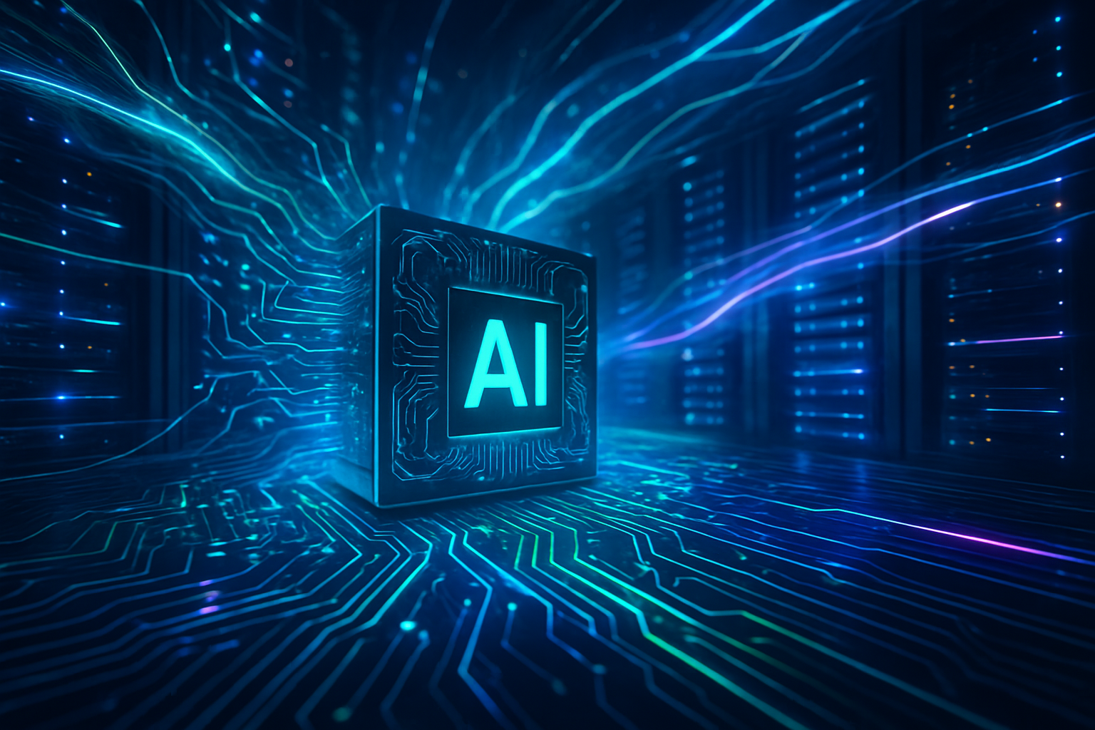
The relentless pursuit of greater computational power for Artificial Intelligence (AI) has pushed the semiconductor industry to its limits. As traditional silicon scaling, epitomized by Moore's Law, faces increasing physical and economic hurdles, a new frontier in chip design and manufacturing has emerged: advanced packaging technologies. These innovative techniques are not merely incremental improvements; they represent a fundamental redefinition of how semiconductors are built, acting as a critical enabler for the next generation of AI hardware and ensuring that the exponential growth of AI capabilities can continue unabated.
Advanced packaging is rapidly becoming the cornerstone of high-performance AI semiconductors, offering a powerful pathway to overcome the "memory wall" bottleneck and deliver the unprecedented bandwidth, low latency, and energy efficiency demanded by today's sophisticated AI models. By integrating multiple specialized chiplets into a single, compact package, these technologies are unlocking new levels of performance that monolithic chip designs can no longer achieve alone. This paradigm shift is crucial for everything from massive data center AI accelerators powering large language models to energy-efficient edge AI devices, marking a pivotal moment in the ongoing AI revolution.
The Architectural Revolution: Deconstructing and Rebuilding for AI Dominance
The core of advanced packaging's breakthrough lies in its ability to move beyond the traditional monolithic integrated circuit, instead embracing heterogeneous integration. This involves combining various semiconductor dies, or "chiplets," often with different functionalities—such as processors, memory, and I/O controllers—into a single, high-performance package. This modular approach allows for optimized components to be brought together, circumventing the limitations of trying to build a single, ever-larger, and more complex chip.
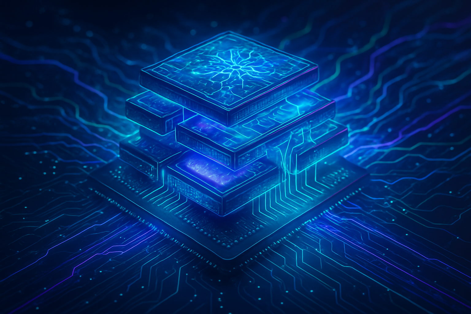
Key technologies driving this shift include 2.5D and 3D-IC (Three-Dimensional Integrated Circuit) packaging. In 2.5D integration, multiple dies are placed side-by-side on a passive silicon or organic interposer, which acts as a high-density wiring board for rapid communication. An exemplary technology in this space is Taiwan Semiconductor Manufacturing Company (TSMC) (NYSE: TSM)'s CoWoS (Chip-on-Wafer-on-Substrate), which has been instrumental in powering leading AI accelerators. 3D-IC integration takes this a step further by stacking multiple semiconductor dies vertically, using Through-Silicon Vias (TSVs) to create direct electrical connections that pass through the silicon layers. This vertical stacking dramatically shortens data pathways, leading to significantly higher bandwidth and lower latency. High-Bandwidth Memory (HBM) is a prime example of 3D-IC technology, where multiple DRAM chips are stacked and connected via TSVs, offering vastly superior memory bandwidth compared to traditional DDR memory. For instance, the NVIDIA (NASDAQ: NVDA) Hopper H200 GPU leverages six HBM stacks to achieve interconnection speeds up to 4.8 terabytes per second, a feat unimaginable with conventional packaging.
This modular, multi-dimensional approach fundamentally differs from previous reliance on shrinking individual transistors on a single chip. While transistor scaling continues, its benefits are diminishing, and its costs are skyrocketing. Advanced packaging offers an alternative vector for performance improvement, allowing designers to optimize different components independently and then integrate them seamlessly. Initial reactions from the AI research community and industry experts have been overwhelmingly positive, with many hailing advanced packaging as the "new Moore's Law" – a critical pathway to sustain the performance gains necessary for the exponential growth of AI. Companies like Intel (NASDAQ: INTC), AMD (NASDAQ: AMD), and Samsung (KRX: 005930) are heavily investing in their own proprietary advanced packaging solutions, recognizing its strategic importance.
Reshaping the AI Landscape: A New Competitive Battleground
The rise of advanced packaging technologies is profoundly impacting AI companies, tech giants, and startups alike, creating a new competitive battleground in the semiconductor space. Companies with robust advanced packaging capabilities or strong partnerships in this area stand to gain significant strategic advantages. NVIDIA, a dominant player in AI accelerators, has long leveraged advanced packaging, particularly HBM integration, to maintain its performance lead. Its Hopper and upcoming Blackwell architectures are prime examples of how sophisticated packaging translates directly into market-leading AI compute.
Other major AI labs and tech companies are now aggressively pursuing similar strategies. AMD, with its MI series of accelerators, is also a strong proponent of chiplet architecture and advanced packaging, directly challenging NVIDIA's dominance. Intel, through its IDM 2.0 strategy, is investing heavily in its own advanced packaging technologies like Foveros and EMIB, aiming to regain leadership in high-performance computing and AI. Chip foundries like TSMC and Samsung are pivotal players, as their advanced packaging services are indispensable for fabless AI chip designers. Startups developing specialized AI accelerators also benefit, as advanced packaging allows them to integrate custom logic with off-the-shelf high-bandwidth memory, accelerating their time to market and improving performance.
This development has the potential to disrupt existing products and services by enabling more powerful, efficient, and cost-effective AI hardware. Companies that fail to adopt or innovate in advanced packaging may find their products lagging in performance and power efficiency. The ability to integrate diverse functionalities—from custom AI accelerators to high-speed memory and specialized I/O—into a single package offers unparalleled flexibility, allowing companies to tailor solutions precisely for specific AI workloads, thereby enhancing their market positioning and competitive edge.
A New Pillar for the AI Revolution: Broader Significance and Implications
Advanced packaging fits seamlessly into the broader AI landscape, serving as a critical hardware enabler for the most significant trends in artificial intelligence. The exponential growth of large language models (LLMs) and generative AI, which demand unprecedented amounts of compute and memory bandwidth, would be severely hampered without these packaging innovations. It provides the physical infrastructure necessary to scale these models effectively, both in terms of performance and energy efficiency.
The impacts are wide-ranging. For AI development, it means researchers can tackle even larger and more complex models, pushing the boundaries of what AI can achieve. For data centers, it translates to higher computational density and lower power consumption per unit of work, addressing critical sustainability concerns. For edge AI, it enables more powerful and capable devices, bringing sophisticated AI closer to the data source and enabling real-time applications in autonomous vehicles, smart factories, and consumer electronics. However, potential concerns include the increasing complexity and cost of advanced packaging processes, which could raise the barrier to entry for smaller players. Supply chain vulnerabilities associated with these highly specialized manufacturing steps also warrant attention.
Compared to previous AI milestones, such as the rise of GPUs for deep learning or the development of specialized AI ASICs, advanced packaging represents a foundational shift. It's not just about a new type of processor but a new way of making processors work together more effectively. It addresses the fundamental physical limitations that threatened to slow down AI progress, much like how the invention of the transistor or the integrated circuit propelled earlier eras of computing. This is a testament to the fact that AI advancements are not solely software-driven but are deeply intertwined with continuous hardware innovation.
The Road Ahead: Anticipating Future Developments and Challenges
The trajectory for advanced packaging in AI semiconductors points towards even greater integration and sophistication. Near-term developments are expected to focus on further refinements in 3D stacking technologies, including hybrid bonding for even denser and more efficient connections between stacked dies. We can also anticipate the continued evolution of chiplet ecosystems, where standardized interfaces will allow different vendors to combine their specialized chiplets into custom, high-performance systems. Long-term, research is exploring photonics integration within packages, leveraging light for ultra-fast communication between chips, which could unlock unprecedented bandwidth and energy efficiency gains.
Potential applications and use cases on the horizon are vast. Beyond current AI accelerators, advanced packaging will be crucial for specialized neuromorphic computing architectures, quantum computing integration, and highly distributed edge AI systems that require immense processing power in miniature form factors. It will enable truly heterogeneous computing environments where CPUs, GPUs, FPGAs, and custom AI accelerators coexist and communicate seamlessly within a single package.
However, significant challenges remain. The thermal management of densely packed, high-power chips is a critical hurdle, requiring innovative cooling solutions. Ensuring robust interconnect reliability and managing the increased design complexity are also ongoing tasks. Furthermore, the cost of advanced packaging processes can be substantial, necessitating breakthroughs in manufacturing efficiency. Experts predict that the drive for modularity and integration will intensify, with a focus on standardizing chiplet interfaces to foster a more open and collaborative ecosystem, potentially democratizing access to cutting-edge hardware components.
A New Horizon for AI Hardware: The Indispensable Role of Advanced Packaging
In summary, advanced packaging technologies have unequivocally emerged as an indispensable pillar supporting the continued advancement of Artificial Intelligence. By effectively circumventing the diminishing returns of traditional transistor scaling, these innovations—from 2.5D interposers and HBM to sophisticated 3D stacking—are providing the crucial bandwidth, latency, and power efficiency gains required by modern AI workloads, especially the burgeoning field of generative AI and large language models. This architectural shift is not merely an optimization; it is a fundamental re-imagining of how high-performance chips are designed and integrated, ensuring that hardware innovation keeps pace with the breathtaking progress in AI algorithms.
The significance of this development in AI history cannot be overstated. It represents a paradigm shift as profound as the move from single-core to multi-core processors, or the adoption of GPUs for general-purpose computing. It underscores the symbiotic relationship between hardware and software in AI, demonstrating that breakthroughs in one often necessitate, and enable, breakthroughs in the other. As the industry moves forward, the ability to master and innovate in advanced packaging will be a key differentiator for semiconductor companies and AI developers alike.
In the coming weeks and months, watch for continued announcements regarding new AI accelerators leveraging cutting-edge packaging techniques, further investments from major tech companies into their advanced packaging capabilities, and the potential for new industry collaborations aimed at standardizing chiplet interfaces. The future of AI performance is intrinsically linked to these intricate, multi-layered marvels of engineering, and the race to build the most powerful and efficient AI hardware will increasingly be won or lost in the packaging facility as much as in the fabrication plant.
This content is intended for informational purposes only and represents analysis of current AI developments.
TokenRing AI delivers enterprise-grade solutions for multi-agent AI workflow orchestration, AI-powered development tools, and seamless remote collaboration platforms.
For more information, visit https://www.tokenring.ai/.