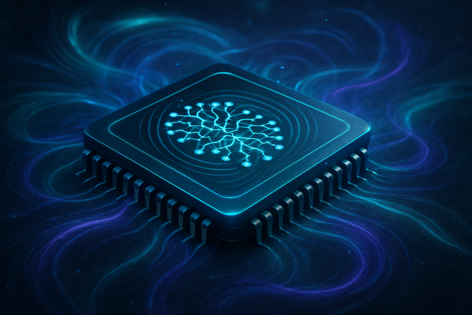
The relentless march of artificial intelligence into every facet of technology and society is underpinned by a less visible, yet utterly critical, force: semiconductor innovation. These tiny chips, the foundational building blocks of all digital computation, are not merely components but the very accelerators of the AI revolution. As AI models grow exponentially in complexity and data demands, the pressure on semiconductor manufacturers to deliver faster, more efficient, and more specialized processing units intensifies, creating a symbiotic relationship where breakthroughs in one field directly propel the other.
This dynamic interplay has never been more evident than in the current landscape, where the burgeoning demand for AI, particularly generative AI and large language models, is driving an unprecedented boom in the semiconductor market. Companies are pouring vast resources into developing next-generation chips tailored for AI workloads, optimizing for parallel processing, energy efficiency, and high-bandwidth memory. The immediate significance of this innovation is profound, leading to an acceleration of AI capabilities across industries, from scientific discovery and autonomous systems to healthcare and finance. Without the continuous evolution of semiconductor technology, the ambitious visions for AI would remain largely theoretical, highlighting the silicon backbone's indispensable role in transforming AI from a specialized technology into a foundational pillar of the global economy.
Powering the Future: NVTS-Nvidia and the DGX Spark Initiative
The intricate dance between semiconductor innovation and AI advancement is perfectly exemplified by strategic partnerships and pioneering hardware initiatives. A prime illustration of this synergy is the collaboration between Navitas Semiconductor (NVTS) (NASDAQ: NVTS) and Nvidia (NASDAQ: NVDA), alongside Nvidia's groundbreaking DGX Spark program. These developments underscore how specialized power delivery and integrated, high-performance computing platforms are pushing the boundaries of what AI can achieve.
The NVTS-Nvidia collaboration, while not a direct chip fabrication deal in the traditional sense, highlights the critical role of power management in high-performance AI systems. Navitas Semiconductor specializes in gallium nitride (GaN) and silicon carbide (SiC) power semiconductors. These advanced materials offer significantly higher efficiency and power density compared to traditional silicon-based power electronics. For AI data centers, which consume enormous amounts of electricity, integrating GaN and SiC power solutions means less energy waste, reduced cooling requirements, and ultimately, more compact and powerful server designs. This allows for greater computational density within the same footprint, directly supporting the deployment of more powerful AI accelerators like Nvidia's GPUs. This differs from previous approaches that relied heavily on less efficient silicon power components, leading to larger power supplies, more heat, and higher operational costs. Initial reactions from the AI research community and industry experts emphasize the importance of such efficiency gains, noting that sustainable scaling of AI infrastructure is impossible without innovations in power delivery.
Complementing this, Nvidia's DGX Spark program represents a significant leap in AI infrastructure. The DGX Spark is not a single product but an initiative to create fully integrated, enterprise-grade AI supercomputing solutions, often featuring Nvidia's most advanced GPUs (like the H100 or upcoming Blackwell series) interconnected with high-speed networking and sophisticated software stacks. The "Spark" aspect often refers to early access programs or specialized deployments designed to push the envelope of AI research and development. These systems are designed to handle the most demanding AI workloads, such as training colossal large language models (LLMs) with trillions of parameters or running complex scientific simulations. Technically, DGX systems integrate multiple GPUs, NVLink interconnects for ultra-fast GPU-to-GPU communication, and high-bandwidth memory, all optimized within a unified architecture. This integrated approach offers a stark contrast to assembling custom AI clusters from disparate components, providing a streamlined, high-performance, and scalable solution. Experts laud the DGX Spark initiative for democratizing access to supercomputing-level AI capabilities for enterprises and researchers, accelerating breakthroughs that would otherwise be hampered by infrastructure complexities.
Reshaping the AI Landscape: Competitive Implications and Market Dynamics
The innovations embodied by the NVTS-Nvidia synergy and the DGX Spark initiative are not merely technical feats; they are strategic maneuvers that profoundly reshape the competitive landscape for AI companies, tech giants, and startups alike. These advancements solidify the positions of certain players while simultaneously creating new opportunities and challenges across the industry.
Nvidia (NASDAQ: NVDA) stands as the unequivocal primary beneficiary of these developments. Its dominance in the AI chip market is further entrenched by its ability to not only produce cutting-edge GPUs but also to build comprehensive, integrated AI platforms like the DGX series. By offering complete solutions that combine hardware, software (CUDA), and networking, Nvidia creates a powerful ecosystem that is difficult for competitors to penetrate. The DGX Spark program, in particular, strengthens Nvidia's ties with leading AI research institutions and enterprises, ensuring its hardware remains at the forefront of AI development. This strategic advantage allows Nvidia to dictate industry standards and capture a significant portion of the rapidly expanding AI infrastructure market.
For other tech giants and AI labs, the implications are varied. Companies like Google (NASDAQ: GOOGL) and Amazon (NASDAQ: AMZN), which are heavily invested in their own custom AI accelerators (TPUs and Inferentia/Trainium, respectively), face continued pressure to match Nvidia's performance and ecosystem. While their internal chips offer optimization for their specific cloud services, Nvidia's broad market presence and continuous innovation force them to accelerate their own development cycles. Startups, on the other hand, often rely on readily available, powerful hardware to develop and deploy their AI solutions. The availability of highly optimized systems like DGX Spark, even through cloud providers, allows them to access supercomputing capabilities without the prohibitive cost and complexity of building their own from scratch, fostering innovation across the startup ecosystem. However, this also means many startups are inherently tied to Nvidia's ecosystem, creating a dependency that could have long-term implications for diversity in AI hardware.
The potential disruption to existing products and services is significant. As AI capabilities become more powerful and accessible through optimized hardware, industries reliant on less sophisticated AI or traditional computing methods will need to adapt. For instance, enhanced generative AI capabilities powered by advanced semiconductors could disrupt content creation, drug discovery, and engineering design workflows. Companies that fail to leverage these new hardware capabilities to integrate cutting-edge AI into their offerings risk falling behind. Market positioning becomes crucial, with companies that can quickly adopt and integrate these new semiconductor-driven AI advancements gaining a strategic advantage. This creates a competitive imperative for continuous investment in AI infrastructure and talent, further intensifying the race to the top in the AI arms race.
The Broader Canvas: AI's Trajectory and Societal Impacts
The relentless evolution of semiconductor technology, epitomized by advancements like efficient power delivery for AI and integrated supercomputing platforms, paints a vivid picture of AI's broader trajectory. These developments are not isolated events but crucial milestones within the grand narrative of artificial intelligence, shaping its future and profoundly impacting society.
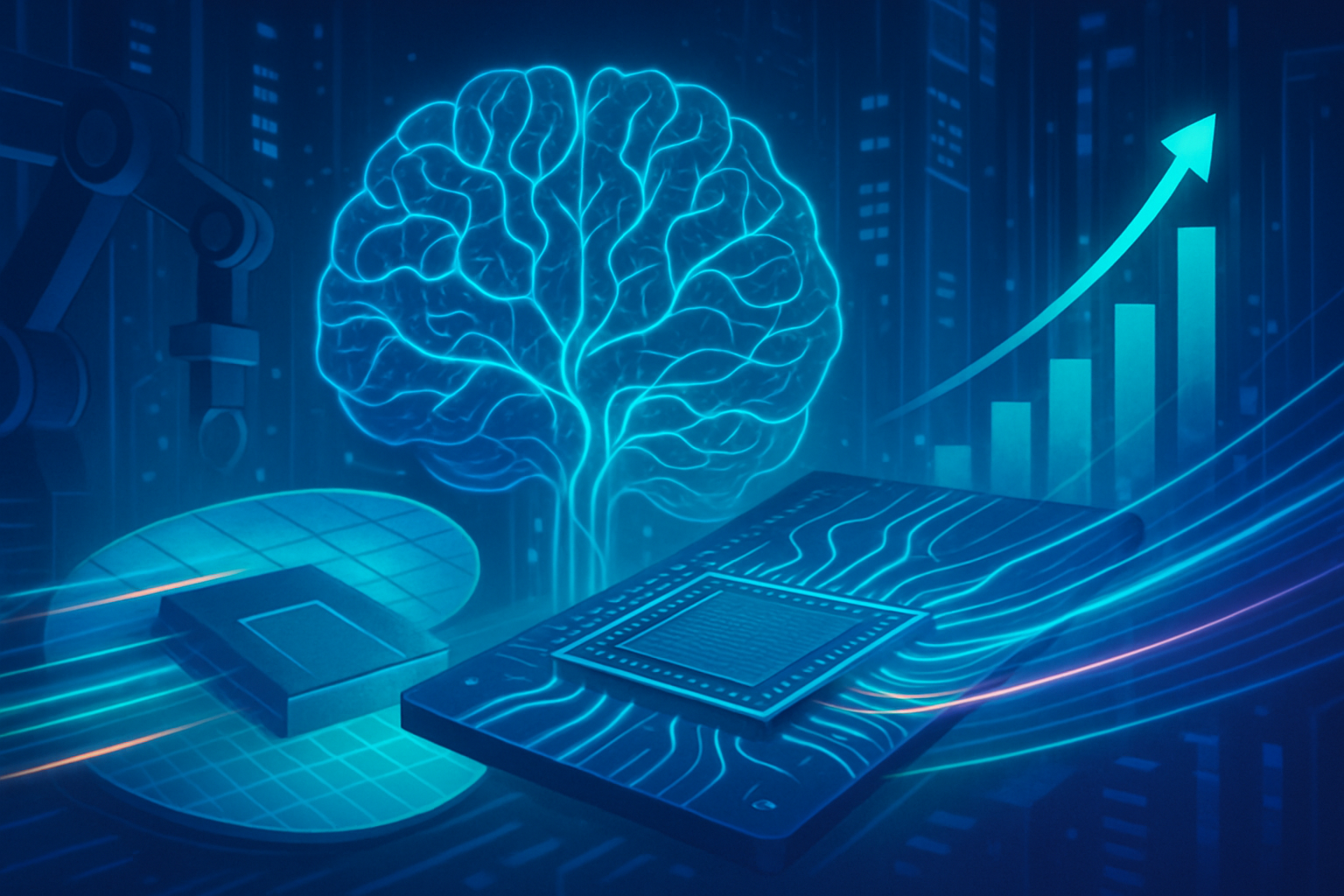
These innovations fit squarely into the broader AI landscape's trend towards greater computational intensity and specialization. The ability to efficiently power and deploy massive AI models is directly enabling the continued scaling of large language models (LLMs), multimodal AI, and sophisticated autonomous systems. This pushes the boundaries of what AI can perceive, understand, and generate, moving us closer to truly intelligent machines. The focus on energy efficiency, driven by GaN and SiC power solutions, also aligns with a growing industry concern for sustainable AI, addressing the massive carbon footprint of training ever-larger models. Comparisons to previous AI milestones, such as the development of early neural networks or the ImageNet moment, reveal a consistent pattern: hardware breakthroughs have always been critical enablers of algorithmic advancements. Today's semiconductor innovations are fueling the "AI supercycle," accelerating progress at an unprecedented pace.
The impacts are far-reaching. On the one hand, these advancements promise to unlock solutions to some of humanity's most pressing challenges, from accelerating drug discovery and climate modeling to revolutionizing education and accessibility. The enhanced capabilities of AI, powered by superior semiconductors, will drive unprecedented productivity gains and create entirely new industries and job categories. However, potential concerns also emerge. The immense computational power concentrated in a few hands raises questions about AI governance, ethical deployment, and the potential for misuse. The "AI divide" could widen, where nations or entities with access to cutting-edge semiconductor technology and AI expertise gain significant advantages over those without. Furthermore, the sheer energy consumption of AI, even with efficiency improvements, remains a significant environmental consideration, necessitating continuous innovation in both hardware and software optimization. The rapid pace of change also poses challenges for regulatory frameworks and societal adaptation, demanding proactive engagement from policymakers and ethicists.
Glimpsing the Horizon: Future Developments and Expert Predictions
Looking ahead, the symbiotic relationship between semiconductors and AI promises an even more dynamic and transformative future. Experts predict a continuous acceleration in both fields, with several key developments on the horizon.
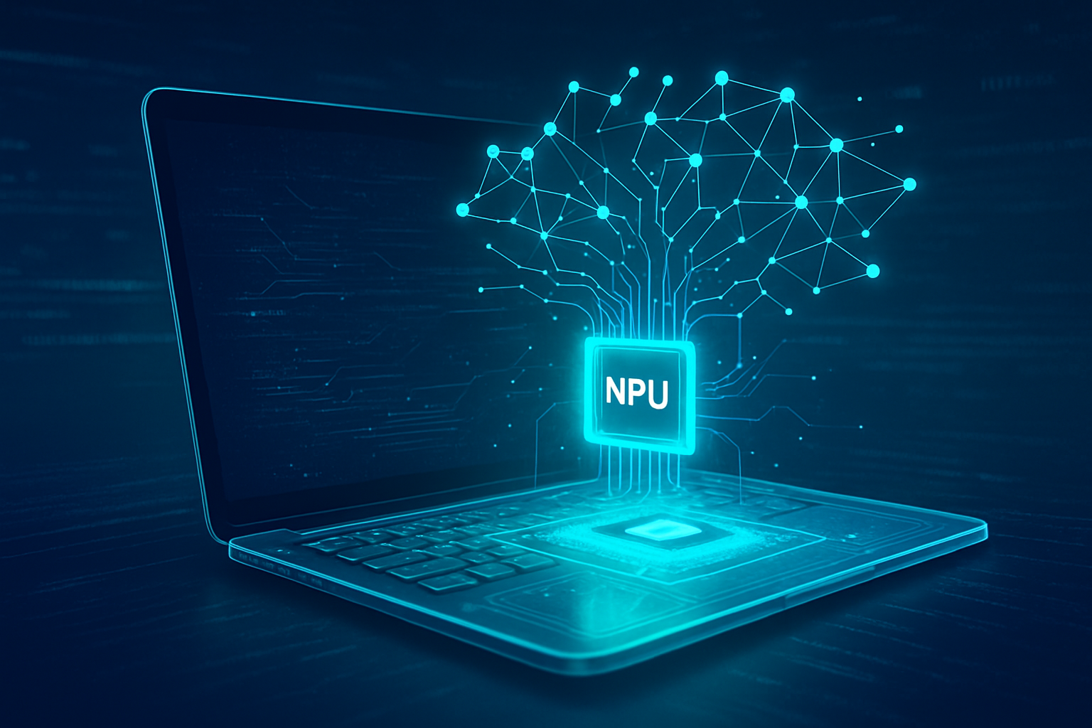
In the near term, we can expect continued advancements in specialized AI accelerators. Beyond current GPUs, the focus will intensify on custom ASICs (Application-Specific Integrated Circuits) designed for specific AI workloads, offering even greater efficiency and performance for tasks like inference at the edge. We will also see further integration of heterogeneous computing, where CPUs, GPUs, NPUs, and other specialized cores are seamlessly combined on a single chip or within a single system to optimize for diverse AI tasks. Memory innovation, particularly High Bandwidth Memory (HBM), will continue to evolve, with higher capacities and faster speeds becoming standard to feed the ever-hungry AI models. Long-term, the advent of novel computing paradigms like neuromorphic chips, which mimic the structure and function of the human brain for ultra-efficient processing, and potentially even quantum computing, could unlock AI capabilities far beyond what is currently imagined. Silicon photonics, using light instead of electrons for data transfer, is also on the horizon to address bandwidth bottlenecks.
Potential applications and use cases are boundless. Enhanced AI, powered by these future semiconductors, will drive breakthroughs in personalized medicine, creating AI models that can analyze individual genomic data to tailor treatments. Autonomous systems, from self-driving cars to advanced robotics, will achieve unprecedented levels of perception and decision-making. Generative AI will become even more sophisticated, capable of creating entire virtual worlds, complex scientific simulations, and highly personalized educational content. Challenges, however, remain. The "memory wall" – the bottleneck between processing units and memory – will continue to be a significant hurdle. Power consumption, despite efficiency gains, will require ongoing innovation. The complexity of designing and manufacturing these advanced chips will also necessitate new AI-driven design tools and manufacturing processes. Experts predict that AI itself will play an increasingly critical role in designing the next generation of semiconductors, creating a virtuous cycle of innovation. The focus will also shift towards making AI more accessible and deployable at the edge, enabling intelligent devices to operate autonomously without constant cloud connectivity.
The Unseen Engine: A Comprehensive Wrap-up of AI's Semiconductor Foundation
The narrative of artificial intelligence in the 2020s is inextricably linked to the silent, yet powerful, revolution occurring within the semiconductor industry. The key takeaway from recent developments, such as the drive for efficient power solutions and integrated AI supercomputing platforms, is that hardware innovation is not merely supporting AI; it is actively defining its trajectory and potential. Without the continuous breakthroughs in chip design, materials science, and manufacturing processes, the ambitious visions for AI would remain largely theoretical.
This development's significance in AI history cannot be overstated. We are witnessing a period where the foundational infrastructure for AI is being rapidly advanced, enabling the scaling of models and the deployment of capabilities that were unimaginable just a few years ago. The shift towards specialized accelerators, combined with a focus on energy efficiency, marks a mature phase in AI hardware development, moving beyond general-purpose computing to highly optimized solutions. This period will likely be remembered as the era when AI transitioned from a niche academic pursuit to a ubiquitous, transformative force, largely on the back of silicon's relentless progress.
Looking ahead, the long-term impact of these advancements will be profound, shaping economies, societies, and even human capabilities. The continued democratization of powerful AI through accessible hardware will accelerate innovation across every sector. However, it also necessitates careful consideration of ethical implications, equitable access, and sustainable practices. What to watch for in the coming weeks and months includes further announcements of next-generation AI accelerators, strategic partnerships between chip manufacturers and AI developers, and the increasing adoption of AI-optimized hardware in cloud data centers and edge devices. The race for AI supremacy is, at its heart, a race for semiconductor superiority, and the finish line is nowhere in sight.
This content is intended for informational purposes only and represents analysis of current AI developments.
TokenRing AI delivers enterprise-grade solutions for multi-agent AI workflow orchestration, AI-powered development tools, and seamless remote collaboration platforms.
For more information, visit https://www.tokenring.ai/.