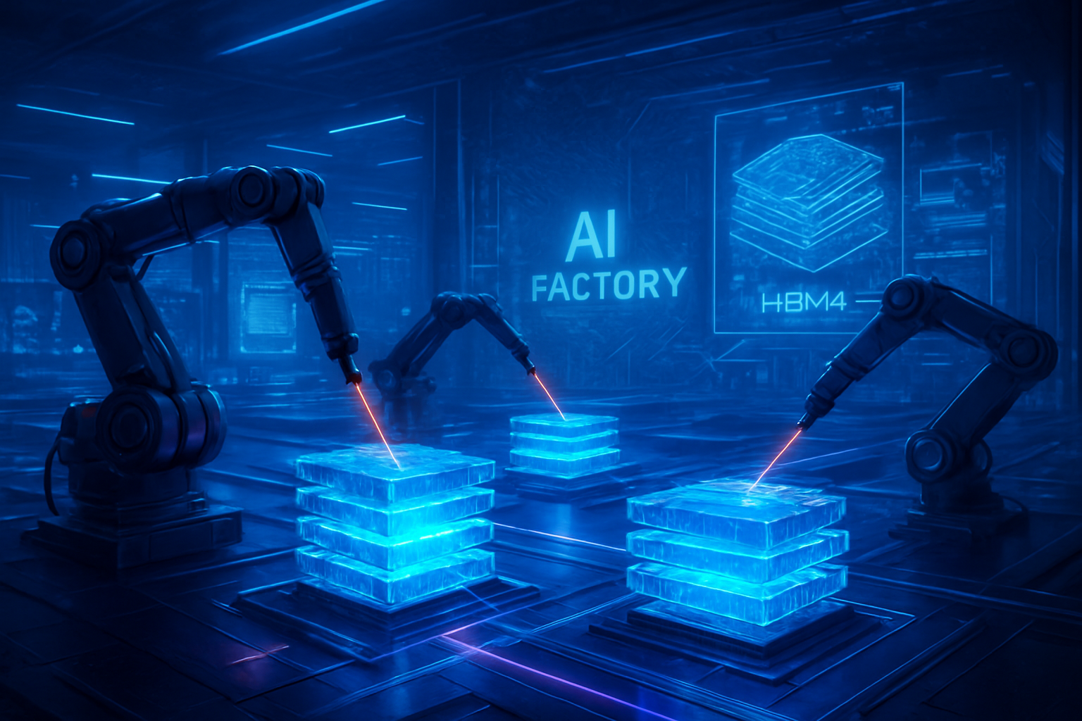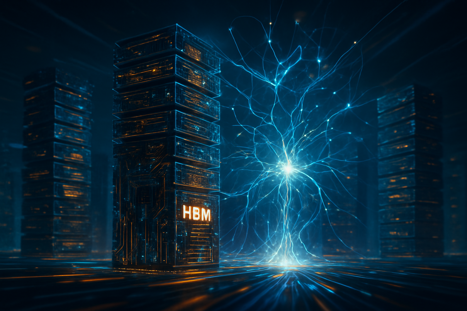
Micron Technology (NASDAQ: MU) has officially confirmed that its entire production capacity for High-Bandwidth Memory (HBM) is fully committed through the end of the 2026 calendar year. This landmark announcement underscores a historic supply-demand imbalance in the semiconductor sector, driven by the insatiable appetite for artificial intelligence infrastructure. As the industry moves into 2026, Micron’s 100% sell-through status signals that the scarcity of specialized memory has become the primary bottleneck for the global rollout of next-generation AI accelerators.
The "sold-out" status comes at a pivotal moment as the tech industry pivots from HBM3E toward the much-anticipated HBM4 standard. This supply lock-in not only guarantees record-shattering revenue for the Boise-based chipmaker but also marks a structural shift in the global memory market. With prices and volumes finalized for the next 22 months, Micron has effectively de-risked its financial outlook while leaving latecomers to the AI race scrambling for a dwindling pool of available silicon.
Technical Leaps and the HBM4 Horizon
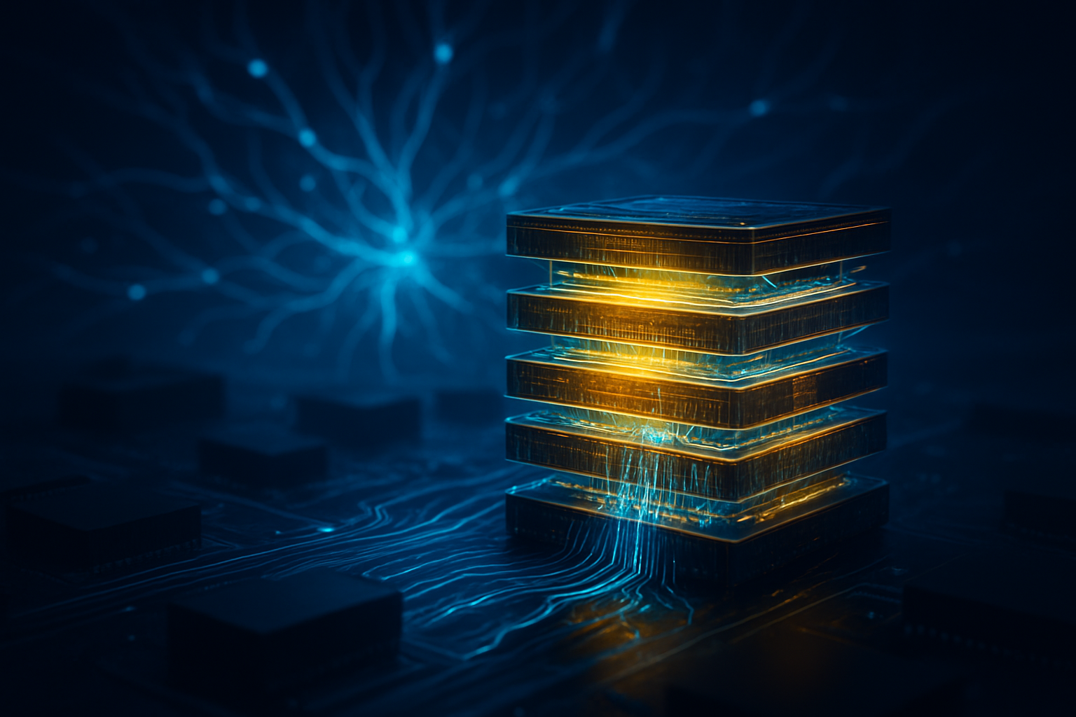
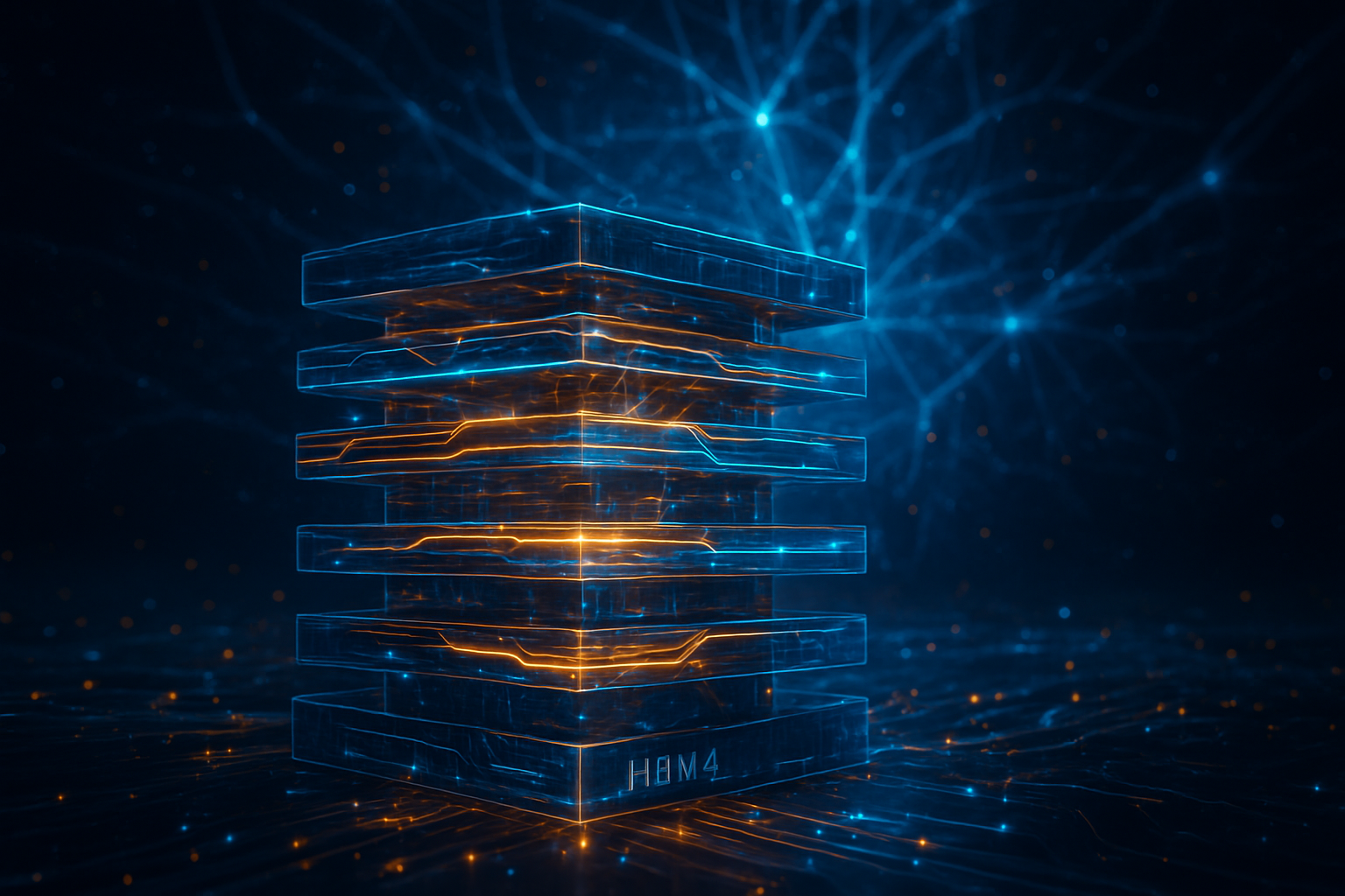
The technical specifications of Micron’s latest offerings represent a quantum leap in data throughput. The current gold standard, HBM3E, which powers the H200 and Blackwell architectures from Nvidia (NASDAQ: NVDA), is already being superseded by HBM4 samples. Micron’s HBM4 modules, currently in the hands of key partners for qualification, are achieving bandwidth speeds of up to 11 Gbps. This performance is achieved using Micron’s proprietary 1β (1-beta) process technology, which allows for higher bit density and significantly lower power consumption compared to the previous 1α generation.
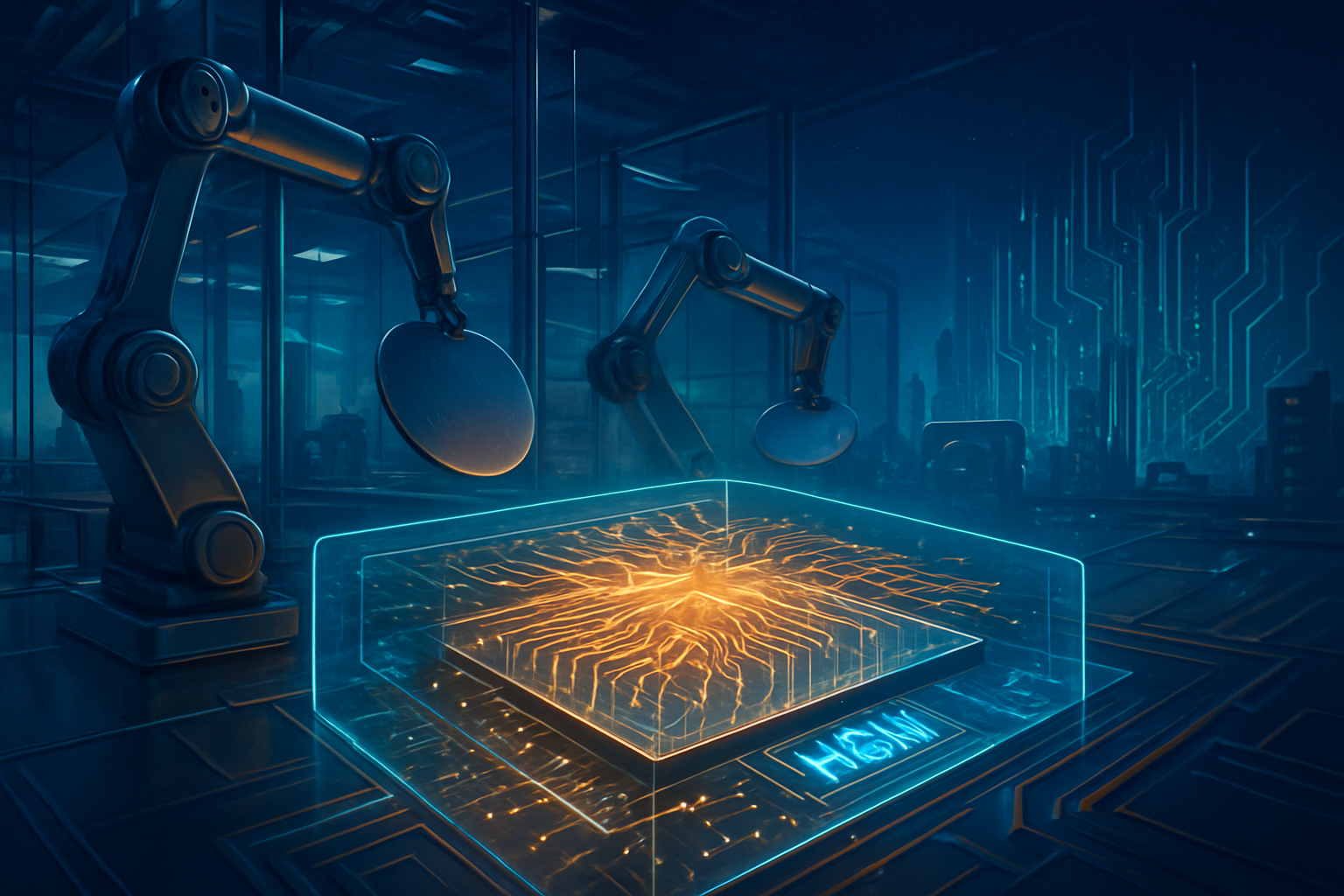
The transition to HBM4 is fundamentally different from prior iterations due to its architectural complexity. For the first time, the "base die" of the memory stack—the logic layer that communicates with the GPU—is being developed in closer collaboration with foundries like Taiwan Semiconductor Manufacturing Company (NYSE: TSM). This "foundry-direct" model allows the memory to be integrated more tightly with the processor, reducing latency and heat. The move to a 2048-bit interface in HBM4, doubling the width of HBM3, is essential to feed the massive computational cores of upcoming AI platforms like Nvidia’s Rubin.
Industry experts note that HBM production is significantly more resource-intensive than traditional DRAM. Manufacturing HBM requires approximately three times the wafer capacity of standard DDR5 memory to produce the same number of bits. This "wafer cannibalization" is the technical root of the current shortage; every HBM chip produced for a data center essentially deletes three chips that could have gone into a consumer laptop or smartphone. This shift has forced Micron to make the radical strategic decision to sunset its consumer-facing Crucial brand in late 2025, redirecting all engineering talent toward high-margin AI enterprise solutions.
Market Dominance and Competitive Moats
The immediate beneficiaries of Micron’s guaranteed supply are the "Big Three" of AI hardware: Nvidia, Advanced Micro Devices (NASDAQ: AMD), and major hyperscalers like Google and Amazon who are developing custom ASICs. By locking in Micron’s capacity, these companies have secured a strategic moat against smaller competitors. However, the 100% sell-through also highlights a precarious dependency. Any yield issues or manufacturing hiccups at Micron’s facilities could now lead to multi-billion-dollar delays in the deployment of AI clusters across the globe.
The competitive landscape among memory providers has reached a fever pitch. While Micron has secured its 2026 roadmap, it faces fierce pressure from SK Hynix (KOSPI: 000660), which currently holds a slight lead in market share and is aiming to supply 70% of the HBM4 requirements for the Nvidia Rubin platform. Simultaneously, Samsung Electronics (KRX: 005930) is staging an aggressive counter-offensive. After trailing in the HBM3E race, Samsung has begun full-scale shipments of its HBM4 modules this February, targeting a bandwidth of 11.7 Gbps to leapfrog its rivals.
This fierce competition for HBM dominance is disrupting traditional market cycles. Memory was once a commodity business defined by boom-and-bust cycles; today, it has become a strategic asset with pricing power that rivals the logic processors themselves. For startups and smaller AI labs, this environment is increasingly hostile. With the three major suppliers (Micron, SK Hynix, and Samsung) fully booked by tech giants, the barrier to entry for training large-scale models continues to rise, potentially consolidating the AI field into a handful of ultra-wealthy players.
Broader Implications: The Great Silicon Reallocation
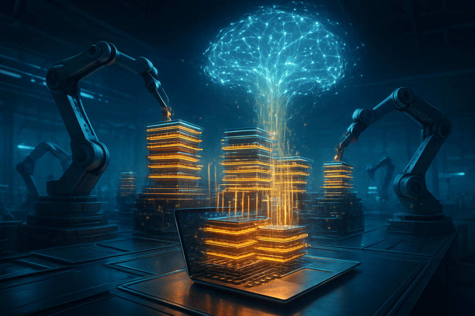
The wider significance of this shortage extends far beyond the data center. The "unprecedented" diversion of manufacturing resources to HBM is beginning to exert inflationary pressure on the entire consumer electronics ecosystem. Analysts predict that PC and smartphone prices could rise by 20% or more by the end of 2026, as the "scraps" of wafer capacity left for standard DRAM become increasingly expensive. We are witnessing a "Great Reallocation" of silicon, where the world’s computing power is being concentrated into centralized AI brains at the expense of edge devices.
In the broader AI landscape, the move to HBM4 marks the end of the "brute force" scaling era and the beginning of the "efficiency-optimized" era. The thermal and power constraints of HBM3E were beginning to hit a ceiling; without the architectural improvements of HBM4, the next generation of AI models would have faced diminishing returns due to data bottlenecks. This milestone is comparable to the transition from mechanical hard drives to SSDs in the early 2010s—a shift that is necessary to unlock the next level of software capability.
However, this reliance on a single, highly complex technology raises concerns about the fragility of the global AI supply chain. The concentration of HBM production in a few specific geographic locations, combined with the extreme difficulty of the manufacturing process, creates a "single point of failure" for the AI revolution. If a major facility were to go offline, the global progress of AI development could effectively grind to a halt for a year or more, given that there is no "Plan B" for high-bandwidth memory.
Future Horizons: Beyond HBM4
Looking ahead, the industry is already eyeing the roadmap for HBM5, which is expected to enter the sampling phase by late 2027. Near-term, the focus will remain on the successful ramp-up of HBM4 mass production in the first half of 2026. Experts predict that the supply-demand imbalance will not find equilibrium until 2028 at the earliest, as new "greenfield" fabrication plants currently under construction in the United States and South Korea take years to reach full capacity.
The next major challenge for Micron and its peers will be the integration of "Optical I/O"—using light instead of electricity to move data between the memory and the processor. While HBM4 pushes the limits of electrical signaling, HBM5 and beyond will likely require a total rethink of how chips are connected. On the application side, we expect to see the emergence of "Memory-Centric Computing," where certain AI processing tasks are moved directly into the HBM stack itself to save energy, a development that would further blur the lines between memory and processor companies.
Conclusion: A High-Stakes Game of Scarcity
The confirmation of Micron’s 100% sell-through for 2026 is a definitive signal that the AI infrastructure boom is far from over. It serves as a stark reminder that the "brains" of the future are built on a foundation of specialized silicon that is currently in critically short supply. The transition to HBM4 is not just a technical upgrade; it is a necessary evolution to sustain the growth of large language models and autonomous systems that define our current era.
As we move through the coming months, the industry will be watching the qualification yields for HBM4 and the financial reports of the major memory players with intense scrutiny. For Micron, the challenge now shifts from finding customers to flawless execution. In a world where every bit of high-bandwidth memory is pre-sold, the ability to manufacture at scale, without error, is the most valuable currency in technology.
This content is intended for informational purposes only and represents analysis of current AI developments.
TokenRing AI delivers enterprise-grade solutions for multi-agent AI workflow orchestration, AI-powered development tools, and seamless remote collaboration platforms. For more information, visit https://www.tokenring.ai/.