The world of microelectronics is currently experiencing an unparalleled surge in technological momentum, a rapid evolution that is not merely incremental but fundamentally transformative, driven almost entirely by the insatiable demands of Artificial Intelligence. As of late 2025, this relentless pace of innovation in chip design, manufacturing, and material science is directly fueling the next generation of AI breakthroughs, promising more powerful, efficient, and ubiquitous intelligent systems across every conceivable sector. This symbiotic relationship sees AI pushing the boundaries of hardware, while advanced hardware, in turn, unlocks previously unimaginable AI capabilities.
Key signals from industry events, including forward-looking insights from upcoming gatherings like Semicon 2025 and reflections from recent forums such as Semicon West 2024, unequivocally highlight Generative AI as the singular, dominant force propelling this technological acceleration. The focus is intensely on overcoming traditional scaling limits through advanced packaging, embracing specialized AI accelerators, and revolutionizing memory architectures. These advancements are immediately significant, enabling the development of larger and more complex AI models, dramatically accelerating training and inference, enhancing energy efficiency, and expanding the frontier of AI applications, particularly at the edge. The industry is not just responding to AI's needs; it's proactively building the very foundation for its exponential growth.
The Engineering Marvels Fueling AI's Ascent
The current technological surge in microelectronics is an intricate dance of engineering marvels, meticulously crafted to meet the voracious demands of AI. This era is defined by a strategic pivot from mere transistor scaling to holistic system-level optimization, embracing advanced packaging, specialized accelerators, and revolutionary memory architectures. These innovations represent a significant departure from previous approaches, enabling unprecedented performance and efficiency.
At the forefront of this revolution is advanced packaging and heterogeneous integration, a critical response to the diminishing returns of traditional Moore's Law. Techniques like 2.5D and 3D integration, exemplified by TSMC's (TPE: 2330) CoWoS (Chip-on-Wafer-on-Substrate) and AMD's (NASDAQ: AMD) MI300X AI accelerator, allow multiple specialized dies—or "chiplets"—to be integrated into a single, high-performance package. Unlike monolithic chips where all functionalities reside on one large die, chiplets enable greater design flexibility, improved manufacturing yields, and optimized performance by minimizing data movement distances. Hybrid bonding further refines 3D integration, creating ultra-fine pitch connections that offer superior electrical performance and power efficiency. Industry experts, including DIGITIMES chief semiconductor analyst Tony Huang, emphasize heterogeneous integration as now "as pivotal to system performance as transistor scaling once was," with strong demand for such packaging solutions through 2025 and beyond.
The rise of specialized AI accelerators marks another significant shift. While GPUs, notably NVIDIA's (NASDAQ: NVDA) H100 and upcoming H200, and AMD's (NASDAQ: AMD) MI300X, remain the workhorses for large-scale AI training due to their massive parallel processing capabilities and dedicated AI instruction sets (like Tensor Cores), the landscape is diversifying. Neural Processing Units (NPUs) are gaining traction for energy-efficient AI inference at the edge, tailoring performance for specific AI tasks in power-constrained environments. A more radical departure comes from neuromorphic chips, such as Intel's (NASDAQ: INTC) Loihi 2, IBM's (NYSE: IBM) TrueNorth, and BrainChip's (ASX: BRN) Akida. These brain-inspired architectures combine processing and memory, offering ultra-low power consumption (e.g., Akida's milliwatt range, Loihi 2's 10x-50x energy savings over GPUs for specific tasks) and real-time, event-driven learning. This non-Von Neumann approach is reaching a "critical inflection point" in 2025, moving from research to commercial viability for specialized applications like cybersecurity and robotics, offering efficiency levels unattainable by conventional accelerators.
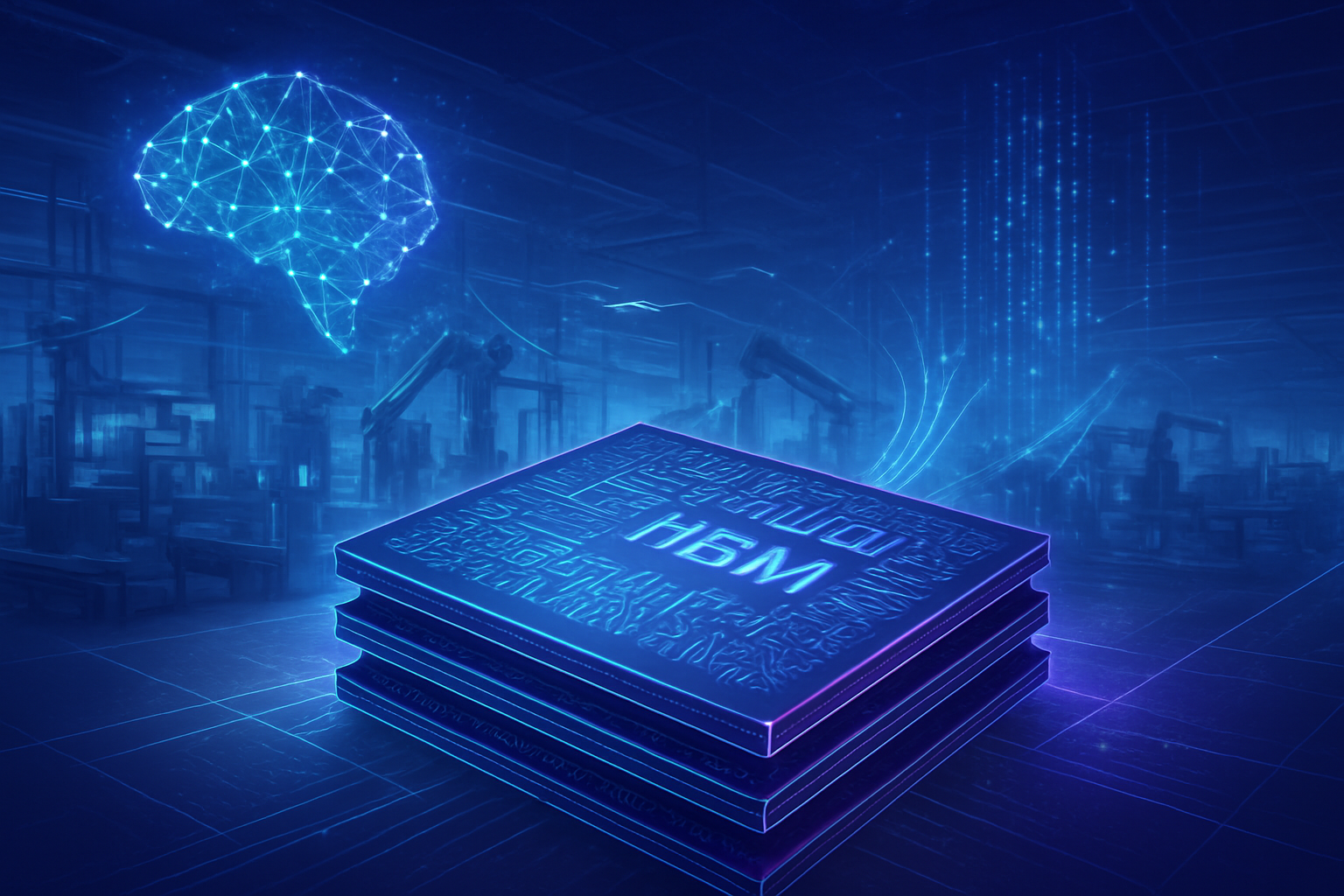
Furthermore, innovations in memory technologies are crucial for overcoming the "memory wall." High Bandwidth Memory (HBM), with its 3D-stacked architecture, provides unprecedented data transfer rates directly to AI accelerators. HBM3E is currently in high demand, with HBM4 expected to sample in 2025, and its capacity from major manufacturers like SK Hynix (KRX: 000660), Samsung (KRX: 005930), and Micron (NASDAQ: MU) reportedly sold out through 2025 and into 2026. This is indispensable for feeding the colossal data needs of Large Language Models (LLMs). Complementing HBM is Compute Express Link (CXL), an open-standard interconnect that enables flexible memory expansion, pooling, and sharing across heterogeneous computing environments. CXL 3.0, released in 2022, allows for memory disaggregation and dynamic allocation, transforming data centers by creating massive, shared memory pools, a significant departure from memory strictly tied to individual processors. While HBM provides ultra-high bandwidth at the chip level, CXL boosts GPU utilization by providing expandable and shareable memory for large context windows.
Finally, advancements in manufacturing processes are pushing the boundaries of what's possible. The transition to 3nm and 2nm process nodes by leaders like TSMC (TPE: 2330) and Samsung (KRX: 005930), incorporating Gate-All-Around FET (GAAFET) architectures, offers superior electrostatic control, leading to further improvements in performance, power efficiency, and area. While incredibly complex and expensive, these nodes are vital for high-performance AI chips. Simultaneously, AI-driven Electronic Design Automation (EDA) tools from companies like Synopsys (NASDAQ: SNPS) and Cadence (NASDAQ: CDNS) are revolutionizing chip design by automating optimization and verification, cutting design timelines from months to weeks. In the fabs, smart manufacturing leverages AI for predictive maintenance, real-time process optimization, and AI-driven defect detection, significantly enhancing yield and efficiency, as seen with TSMC's reported 20% yield increase on 3nm lines after AI implementation. These integrated advancements signify a holistic approach to microelectronics innovation, where every layer of the technology stack is being optimized for the AI era.
A Shifting Landscape: Competitive Dynamics and Strategic Advantages
The current wave of microelectronics innovation is not merely enhancing capabilities; it's fundamentally reshaping the competitive landscape for AI companies, tech giants, and startups alike. The intense demand for faster, more efficient, and scalable AI infrastructure is creating both immense opportunities and significant strategic challenges, particularly as we navigate through 2025.
Semiconductor manufacturers stand as direct beneficiaries. NVIDIA (NASDAQ: NVDA), with its dominant position in AI GPUs and the robust CUDA ecosystem, continues to be a central player, with its Blackwell architecture eagerly anticipated. However, the rapidly growing inference market is seeing increased competition from specialized accelerators. Foundries like TSMC (TPE: 2330) are critical, with their 3nm and 5nm capacities fully booked through 2026 by major players, underscoring their indispensable role in advanced node manufacturing and packaging. Memory giants Samsung (KRX: 005930), SK Hynix (KRX: 000660), and Micron (NASDAQ: MU) are experiencing an explosive surge in demand for High Bandwidth Memory (HBM), which is projected to reach $3.8 billion in 2025 for AI chipsets alone, making them vital partners in the AI supply chain. Other major players like Intel (NASDAQ: INTC), AMD (NASDAQ: AMD), Qualcomm (NASDAQ: QCOM), and Broadcom (NASDAQ: AVGO) are also making substantial investments in AI accelerators and related technologies, vying for market share.
Tech giants are increasingly embracing vertical integration, designing their own custom AI silicon to optimize their cloud infrastructure and AI-as-a-service offerings. Google (NASDAQ: GOOGL) with its TPUs and Axion, Microsoft (NASDAQ: MSFT) with Azure Maia 100 and Cobalt 100, and Amazon (NASDAQ: AMZN) with Trainium and Inferentia, are prime examples. This strategic move provides greater control over hardware optimization, cost efficiency, and performance for their specific AI workloads, offering a significant competitive edge and potentially disrupting traditional GPU providers in certain segments. Apple (NASDAQ: AAPL) continues to leverage its in-house chip design expertise with its M-series chips for on-device AI, with future plans for 2nm technology. For AI startups, while the high cost of advanced packaging and manufacturing remains a barrier, opportunities exist in niche areas like edge AI and specialized accelerators, often through strategic partnerships with memory providers or cloud giants for scalability and financial viability.
The competitive implications are profound. NVIDIA's strong lead in AI training is being challenged in the inference market by specialized accelerators and custom ASICs, which are projected to capture a significant share by 2025. The rise of custom silicon from hyperscalers fosters a more diversified chip design landscape, potentially altering market dynamics for traditional hardware suppliers. Strategic partnerships across the supply chain are becoming paramount due to the complexity of these advancements, ensuring access to cutting-edge technology and optimized solutions. Furthermore, the burgeoning demand for AI chips and HBM risks creating shortages in other sectors, impacting industries reliant on mature technologies. The shift towards edge AI, enabled by power-efficient chips, also presents a potential disruption to cloud-centric AI models by allowing localized, real-time processing.
Companies that can deliver high-performance, energy-efficient, and specialized chips will gain a significant strategic advantage, especially given the rising focus on power consumption in AI infrastructure. Leadership in advanced packaging, securing HBM access, and early adoption of CXL technology are becoming critical differentiators for AI hardware providers. Moreover, the adoption of AI-driven EDA tools from companies like Synopsys (NASDAQ: SNPS) and Cadence (NASDAQ: CDNS), which can cut design cycles from months to weeks, is crucial for accelerating time-to-market. Ultimately, the market is increasingly demanding "full-stack" AI solutions that seamlessly integrate hardware, software, and services, pushing companies to develop comprehensive ecosystems around their core technologies, much like NVIDIA's enduring CUDA platform.
Beyond the Chip: Broader Implications and Looming Challenges
The profound innovations in microelectronics extend far beyond the silicon wafer, fundamentally reshaping the broader AI landscape and ushering in significant societal, economic, and geopolitical transformations as we move through 2025. These advancements are not merely incremental; they represent a foundational shift that defines the very trajectory of artificial intelligence.
These microelectronics breakthroughs are the bedrock for the most prominent AI trends. The insatiable demand for scaling Large Language Models (LLMs) is directly met by the immense data throughput offered by High-Bandwidth Memory (HBM), which is projected to see its revenue reach $21 billion in 2025, a 70% year-over-year increase. Beyond HBM, the industry is actively exploring neuromorphic designs for more energy-efficient processing, crucial as LLM scaling faces potential data limitations. Concurrently, Edge AI is rapidly expanding, with its hardware market projected to surge to $26.14 billion in 2025. This trend, driven by compact, energy-efficient chips and advanced power semiconductors, allows AI to move from distant clouds to local devices, enhancing privacy, speed, and resiliency for applications from autonomous vehicles to smart cameras. Crucially, microelectronics are also central to the burgeoning focus on sustainability in AI. Innovations in cooling, interconnection methods, and wide-bandgap semiconductors aim to mitigate the immense power demands of AI data centers, with AI itself being leveraged to optimize energy consumption within semiconductor manufacturing.
Economically, the AI revolution, powered by these microelectronics advancements, is a colossal engine of growth. The global semiconductor market is expected to surpass $600 billion in 2025, with the AI chip market alone projected to exceed $150 billion. AI-driven automation promises significant operational cost reductions for companies, and looking further ahead, breakthroughs in quantum computing, enabled by advanced microchips, could contribute to a "quantum economy" valued up to $2 trillion by 2035. Societally, AI, fueled by this hardware, is revolutionizing healthcare, transportation, and consumer electronics, promising improved quality of life. However, concerns persist regarding job displacement and exacerbated inequalities if access to these powerful AI resources is not equitable. The push for explainable AI (XAI) becoming standard in 2025 aims to address transparency and trust issues in these increasingly pervasive systems.
Despite the immense promise, the rapid pace of advancement brings significant concerns. The cost of developing and acquiring cutting-edge AI chips and building the necessary data center infrastructure represents a massive financial investment. More critically, energy consumption is a looming challenge; data centers could account for up to 9.1% of U.S. national electricity consumption by 2030, with CO2 emissions from AI accelerators alone forecast to rise by 300% between 2025 and 2029. This unsustainable trajectory necessitates a rapid transition to greener energy and more efficient computing paradigms. Furthermore, the accessibility of AI-specific resources risks creating a "digital stratification" between nations, potentially leading to a "dual digital world order." These concerns are amplified by geopolitical implications, as the manufacturing of advanced semiconductors is highly concentrated in a few regions, creating strategic chokepoints and making global supply chains vulnerable to disruptions, as seen in the U.S.-China rivalry for semiconductor dominance.
Compared to previous AI milestones, the current era is defined by an accelerated innovation cycle where AI not only utilizes chips but actively improves their design and manufacturing, leading to faster development and better performance. This generation of microelectronics also emphasizes specialization and efficiency, with AI accelerators and neuromorphic chips offering drastically lower energy consumption and faster processing for AI tasks than earlier general-purpose processors. A key qualitative shift is the ubiquitous integration (Edge AI), moving AI capabilities from centralized data centers to a vast array of devices, enabling local processing and enhancing privacy. This collective progression represents a "quantum leap" in AI capabilities from 2024 to 2025, enabling more powerful, multimodal generative AI models and hinting at the transformative potential of quantum computing itself, all underpinned by relentless microelectronics innovation.
The Road Ahead: Charting AI's Future Through Microelectronics
As the current wave of microelectronics innovation propels AI forward, the horizon beyond 2025 promises even more radical transformations. The relentless pursuit of higher performance, greater efficiency, and novel architectures will continue to address existing bottlenecks and unlock entirely new frontiers for artificial intelligence.
In the near-term, the evolution of High Bandwidth Memory (HBM) will be critical. With HBM3E rapidly adopted, HBM4 is anticipated around 2025, and HBM5 projected for 2029. These next-generation memories will push bandwidth beyond 1 TB/s and capacity up to 48 GB (HBM4) or 96 GB (HBM5) per stack, becoming indispensable for the increasingly demanding AI workloads. Complementing this, Compute Express Link (CXL) will solidify its role as a transformative interconnect. CXL 3.0, with its fabric capabilities, allows entire racks of servers to function as a unified, flexible AI fabric, enabling dynamic memory assignment and disaggregation, which is crucial for multi-GPU inference and massive language models. Future iterations like CXL 3.1 will further enhance scalability and efficiency.
Looking further out, the miniaturization of transistors will continue, albeit with increasing complexity. 1nm (A10) process nodes are projected by Imec around 2028, with sub-1nm (A7, A5, A2) expected in the 2030s. These advancements will rely on revolutionary transistor architectures like Gate All Around (GAA) nanosheets, forksheet transistors, and Complementary FET (CFET) technology, stacking N- and PMOS devices for unprecedented density. Intel (NASDAQ: INTC) is also aggressively pursuing "Angstrom-era" nodes (20A and 18A) with RibbonFET and backside power delivery. Beyond silicon, advanced materials like silicon carbide (SiC) and gallium nitride (GaN) are becoming vital for power components, offering superior performance for energy-efficient microelectronics, while innovations in quantum computing promise to accelerate chip design and material discovery, potentially revolutionizing AI algorithms themselves by requiring fewer parameters for models and offering a path to more sustainable, energy-efficient AI.
These future developments will enable a new generation of AI applications. We can expect support for training and deploying multi-trillion-parameter models, leading to even more sophisticated LLMs. Data centers and cloud infrastructure will become vastly more efficient and scalable, handling petabytes of data for AI, machine learning, and high-performance computing. Edge AI will become ubiquitous, with compact, energy-efficient chips powering advanced features in everything from smartphones and autonomous vehicles to industrial automation, requiring real-time processing capabilities. Furthermore, these advancements will drive significant progress in real-time analytics, scientific computing, and healthcare, including earlier disease detection and widespread at-home health monitoring. AI will also increasingly transform semiconductor manufacturing itself, through AI-powered Electronic Design Automation (EDA), predictive maintenance, and digital twins.
However, significant challenges loom. The escalating power and cooling demands of AI data centers are becoming critical, with some companies even exploring building their own power plants, including nuclear energy solutions, to support gigawatts of consumption. Efficient liquid cooling systems are becoming essential to manage the increased heat density. The cost and manufacturing complexity of moving to 1nm and sub-1nm nodes are exponentially increasing, with fabrication facilities costing tens of billions of dollars and requiring specialized, ultra-expensive equipment. Quantum tunneling and short-channel effects at these minuscule scales pose fundamental physics challenges. Additionally, interconnect bandwidth and latency will remain persistent bottlenecks, despite solutions like CXL, necessitating continuous innovation. Experts predict a future where AI's ubiquity is matched by a strong focus on sustainability, with greener electronics and carbon-neutral enterprises becoming key differentiators. Memory will continue to be a primary limiting factor, driving tighter integration between chip designers and memory manufacturers. Architectural innovations, including on-chip optical communication and neuromorphic designs, will define the next era, all while the industry navigates the critical need for a skilled workforce and resilient supply chains.
A New Era of Intelligence: The Microelectronics-AI Symbiosis
The year 2025 stands as a testament to the profound and accelerating synergy between microelectronics and artificial intelligence. The relentless innovation in chip design, manufacturing, and memory solutions is not merely enhancing AI; it is fundamentally redefining its capabilities and trajectory. This era marks a decisive pivot from simply scaling transistor density to a more holistic approach of specialized hardware, advanced packaging, and novel computing paradigms, all meticulously engineered to meet the insatiable demands of increasingly complex AI models.
The key takeaways from this technological momentum are clear: AI's future is inextricably linked to hardware innovation. Specialized AI accelerators, such as NPUs and custom ASICs, alongside the transformative power of High Bandwidth Memory (HBM) and Compute Express Link (CXL), are directly enabling the training and deployment of massive, sophisticated AI models. The advent of neuromorphic computing is ushering in an era of ultra-energy-efficient, real-time AI, particularly for edge applications. Furthermore, AI itself is becoming an indispensable tool in the design and manufacturing of these advanced chips, creating a virtuous cycle of innovation that accelerates progress across the entire semiconductor ecosystem. This collective push is not just about faster chips; it's about smarter, more efficient, and more sustainable intelligence.
In the long term, these advancements will lead to unprecedented AI capabilities, pervasive AI integration across all facets of life, and a critical focus on sustainability to manage AI's growing energy footprint. New computing paradigms like quantum AI are poised to unlock problem-solving abilities far beyond current limits, promising revolutions in fields from drug discovery to climate modeling. This period will be remembered as the foundation for a truly ubiquitous and intelligent world, where the boundaries between hardware and software continue to blur, and AI becomes an embedded, invisible layer in our technological fabric.
As we move into late 2025 and early 2026, several critical developments bear close watching. The successful mass production and widespread adoption of HBM4 by leading memory manufacturers like Samsung (KRX: 005930) and SK Hynix (KRX: 000660) will be a key indicator of AI hardware readiness. The competitive landscape will be further shaped by the launch of AMD's (NASDAQ: AMD) MI350 series chips and any new roadmaps from NVIDIA (NASDAQ: NVDA), particularly concerning their Blackwell Ultra and Rubin platforms. Pay close attention to the commercialization efforts in in-memory and neuromorphic computing, with real-world deployments from companies like IBM (NYSE: IBM), Intel (NASDAQ: INTC), and BrainChip (ASX: BRN) signaling their viability for edge AI. Continued breakthroughs in 3D stacking and chiplet designs, along with the impact of AI-driven EDA tools on chip development timelines, will also be crucial. Finally, increasing scrutiny on the energy consumption of AI will drive more public benchmarks and industry efforts focused on "TOPS/watt" and sustainable data center solutions.
This content is intended for informational purposes only and represents analysis of current AI developments.
TokenRing AI delivers enterprise-grade solutions for multi-agent AI workflow orchestration, AI-powered development tools, and seamless remote collaboration platforms.
For more information, visit https://www.tokenring.ai/.