As the world rings in early 2026, the artificial intelligence landscape has reached a definitive turning point. NVIDIA (NASDAQ: NVDA) has officially signaled the end of the "Generative Era" and the beginning of the "Agentic Era" with the full-scale transition to its Rubin platform. Unveiled in detail at CES 2026, the Rubin architecture is not merely an incremental update to the record-breaking Blackwell chips of 2025; it is a fundamental redesign of the AI supercomputer. By moving to a six-chip extreme-codesigned architecture, NVIDIA is attempting to solve the most pressing bottleneck of 2026: the cost and complexity of deploying autonomous AI agents at global scale.
The immediate significance of the Rubin launch lies in its promise to reduce the cost of AI inference by nearly tenfold. While the industry spent 2023 through 2025 focused on the raw horsepower needed to train massive Large Language Models (LLMs), the priority has shifted toward "Agentic AI"—systems capable of multi-step reasoning, tool use, and autonomous execution. These workloads require a different kind of compute density and memory bandwidth, which the Rubin platform aims to provide. With the first Rubin-powered racks slated for deployment by major hyperscalers in the second half of 2026, the platform is already resetting expectations for what enterprise AI can achieve.
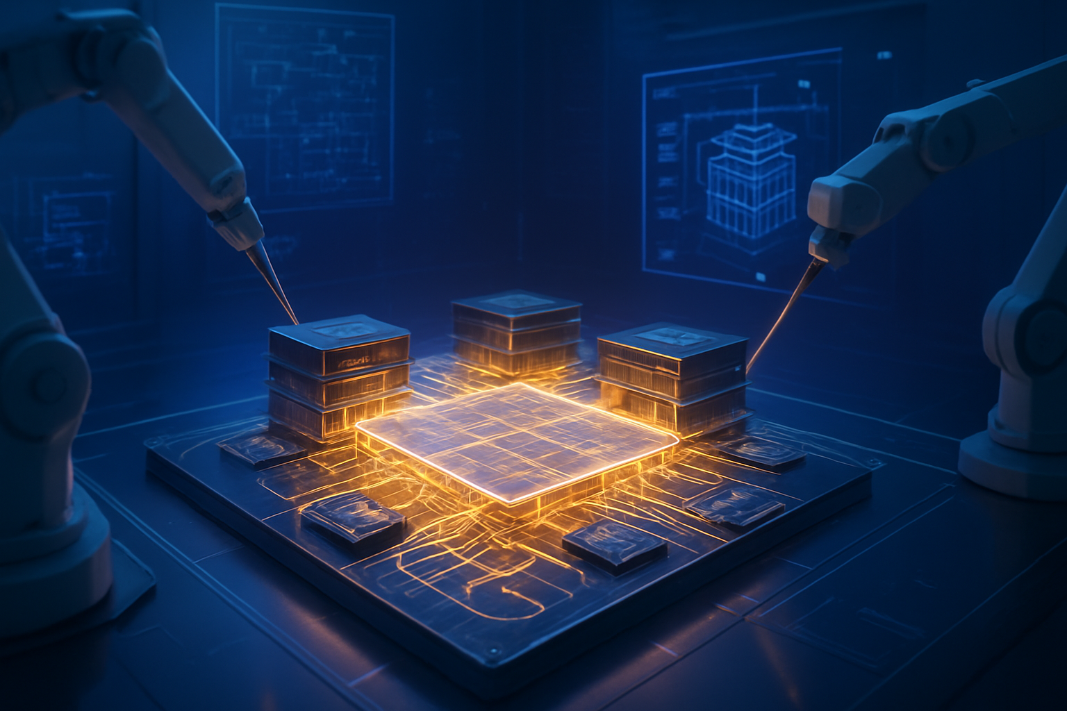
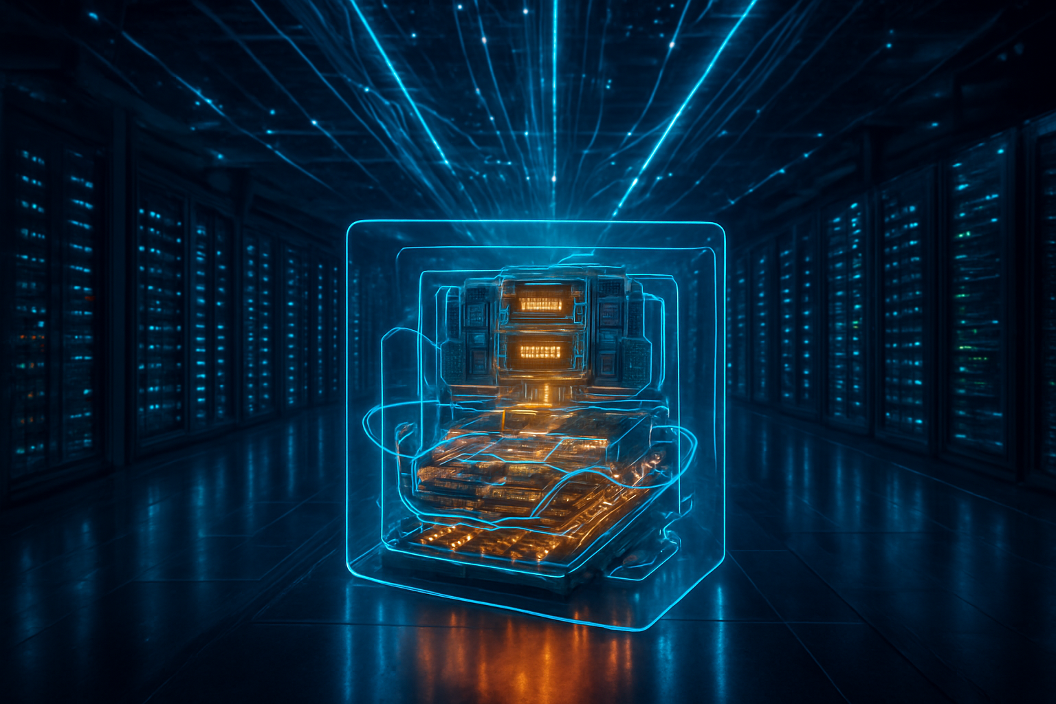
The Six-Chip Symphony: Inside the Rubin Architecture
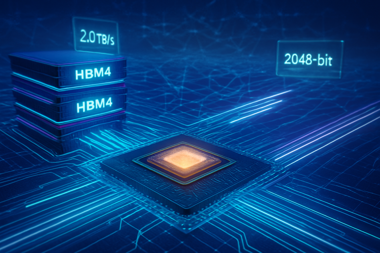
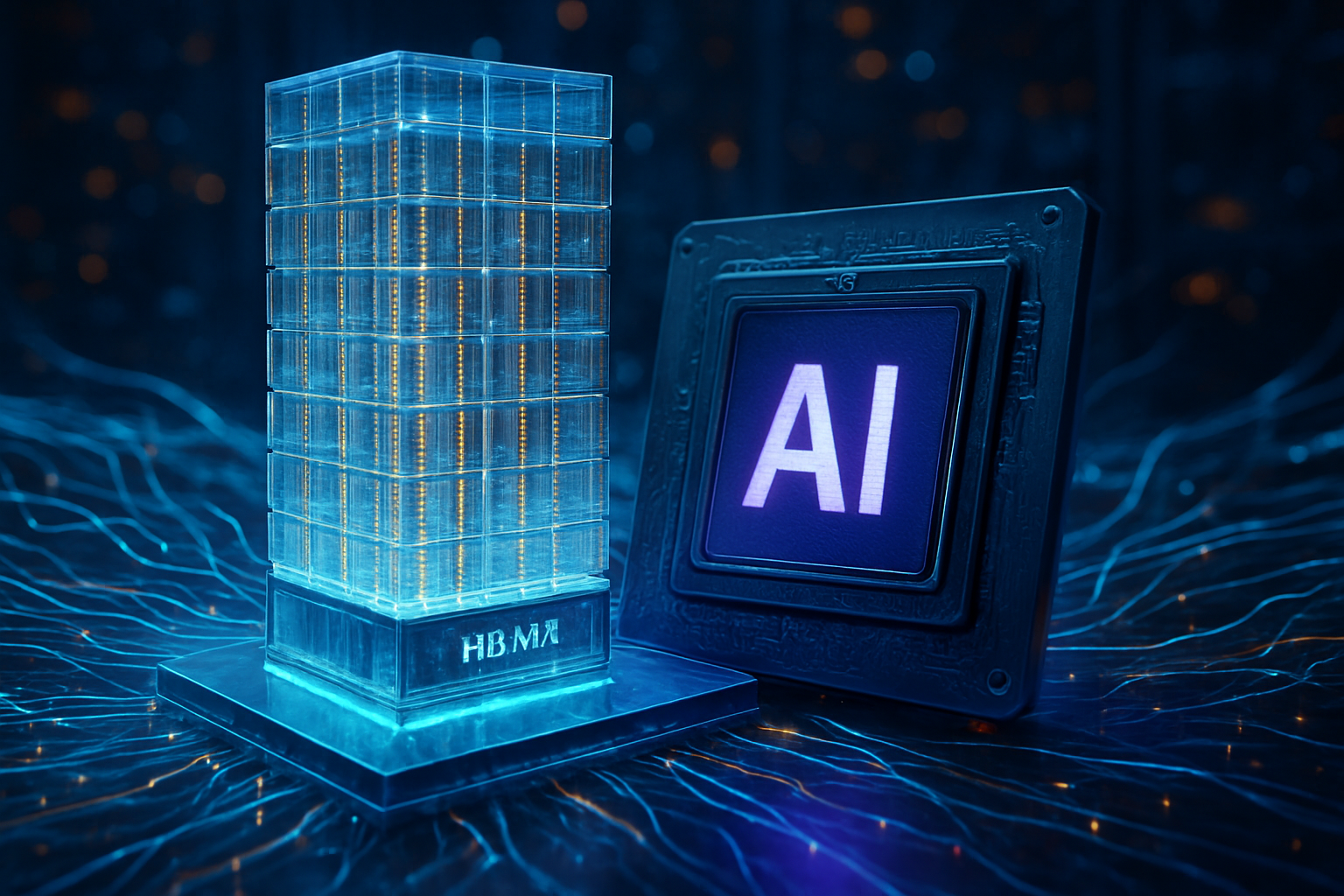
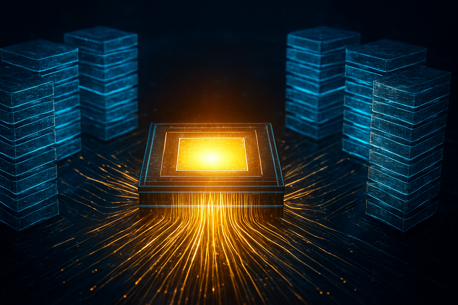
The technical cornerstone of Rubin is its transition to an "extreme-codesigned" architecture. Rather than treating the GPU, CPU, and networking components as separate entities, NVIDIA (NASDAQ: NVDA) has engineered six core silicon elements to function as a single logical unit. This "system-on-rack" approach includes the Rubin GPU, the new Vera CPU, NVLink 6, the ConnectX-9 SuperNIC, the BlueField-4 DPU, and the Spectrum-6 Ethernet Switch. The flagship Rubin GPU features the groundbreaking HBM4 memory standard, doubling the interface width and delivering a staggering 22 TB/s of bandwidth—nearly triple that of the Blackwell generation.
At the heart of the platform sits the Vera CPU, NVIDIA's most ambitious foray into custom silicon. Replacing the Grace architecture, Vera is built on a custom Arm-based "Olympus" core design specifically optimized for the data-orchestration needs of agentic AI. Featuring 88 cores and 176 concurrent threads, Vera is designed to eliminate the "jitter" and latency spikes that can derail real-time autonomous reasoning. When paired with the Rubin GPU via the 1.8 TB/s NVLink-C2C interconnect, the system achieves a level of hardware-software synergy that previously required massive software overhead to manage.
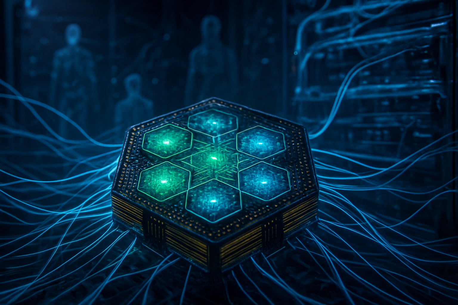
Initial reactions from the AI research community have been centered on Rubin’s "Test-Time Scaling" capabilities. Modern agents often need to "think" longer before answering, generating thousands of internal reasoning tokens to verify a plan. The Rubin platform supports this through the BlueField-4 DPU, which manages up to 150 TB of "Context Memory" per rack. By offloading the Key-Value (KV) cache from the GPU to a dedicated storage layer, Rubin allows agents to maintain multi-million token contexts without starving the compute engine. Industry experts suggest this architecture is the first to truly treat AI memory as a tiered, scalable resource rather than a static buffer.
A New Arms Race: Competitive Fallout and the Hyperscale Response
The launch of Rubin has forced competitors to refine their strategies. Advanced Micro Devices (NASDAQ: AMD) is countering with its Instinct MI400 series, which focuses on a "high-capacity" play. AMD’s MI455X boasts up to 432GB of HBM4 memory—significantly more than the base Rubin GPU—making it a preferred choice for researchers working on massive, non-compressed models. However, AMD is fighting an uphill battle against NVIDIA’s vertically integrated stack. To compensate, AMD is championing the "UALink" and "Ultra Ethernet" open standards, positioning itself as the flexible alternative to NVIDIA’s proprietary ecosystem.
Meanwhile, Intel (NASDAQ: INTC) has pivoted its data center strategy toward "Jaguar Shores," a rack-scale system that mirrors NVIDIA’s integrated approach but focuses on a "unified memory" architecture using Intel’s 18A manufacturing process. While Intel remains behind in the raw performance race as of January 2026, its focus on "Edge AI" and sovereign compute clusters has allowed it to secure a foothold in the European and Asian markets, where data residency and manufacturing independence are paramount.
The major hyperscalers—Microsoft (NASDAQ: MSFT), Alphabet (NASDAQ: GOOGL), Amazon (NASDAQ: AMZN), and Meta Platforms (NASDAQ: META)—are navigating a complex relationship with NVIDIA. Microsoft remains the largest adopter, building its "Fairwater" superfactories specifically to house Rubin NVL72 racks. However, the "NVIDIA Tax" continues to drive these giants to develop their own silicon. Amazon’s Trainium3 and Google’s TPU v7 are now handling a significant portion of their internal, well-defined inference workloads. The Rubin platform’s strategic advantage is its versatility; while custom ASICs are excellent for specific tasks, Rubin is the "Swiss Army Knife" for the unpredictable, reasoning-heavy workloads that define the new agentic frontier.
Beyond the Chips: Sovereignty, Energy, and the Physical AI Shift
The Rubin transition is unfolding against a broader backdrop of "Physical AI" and a global energy crisis. By early 2026, the focus of the AI world has moved from digital chat into the physical environment. Humanoid robots and autonomous industrial systems now rely on the same high-performance inference that Rubin provides. The ability to process "world models"—AI that understands physics and 3D space—requires the extreme memory bandwidth that HBM4 and Rubin provide. This shift has turned the "compute-to-population" ratio into a new metric of national power, leading to the rise of "Sovereign AI" clusters in regions like France, the UAE, and India.
However, the power demands of these systems have reached a fever pitch. A single Rubin-powered data center can consume as much electricity as a small city. This has led to a pivot toward modular nuclear reactors (SMRs) and advanced liquid cooling technologies. NVIDIA’s NVL72 and NVL144 systems are now designed for "warm-water cooling," allowing data centers to operate without the energy-intensive chillers used in previous decades. The broader significance of Rubin is thus as much about thermal efficiency as it is about FLOPS; it is an architecture designed for a world where power is the ultimate constraint.
Concerns remain regarding vendor lock-in and the potential for a "demand air pocket" if the ROI on agentic AI does not materialize as quickly as the infrastructure is built. Critics argue that by controlling the CPU, GPU, and networking, NVIDIA is creating a "walled garden" that could stifle innovation in alternative architectures. Nonetheless, the sheer performance leap—delivering 50 PetaFLOPS of FP4 inference—has, for now, silenced most skeptics who were predicting an end to the AI boom.
Looking Ahead: The Road to Rubin Ultra and Feynman
NVIDIA’s roadmap suggests that the Rubin era is just the beginning. The company has already teased "Rubin Ultra" for 2027, which will transition to HBM4e memory and an even denser NVL576 rack configuration. Beyond that, the "Feynman" architecture planned for 2028 is rumored to target a 30x performance increase over the Blackwell generation, specifically aiming for the thresholds required for Artificial Superintelligence (ASI).
In the near term, the industry will be watching the second-half 2026 rollout of Rubin systems very closely. The primary challenge will be the supply chain; securing enough HBM4 capacity and advanced packaging space at TSMC remains a bottleneck. Furthermore, as AI agents become more autonomous, the industry will face new regulatory and safety hurdles. The ability of Rubin’s hardware-level security features, built into the BlueField-4 DPU, to manage "agentic drift" will be a key area of study for researchers.
A Legacy of Integration: Final Thoughts on the Rubin Transition
The transition to the Rubin platform marks a historical moment in computing history. It is the moment when the GPU transitioned from being a "coprocessor" to becoming the core of a unified, heterogeneous supercomputing system. By codesigning every aspect of the stack, NVIDIA (NASDAQ: NVDA) has effectively reset the ceiling for what is possible in AI inference and autonomous reasoning.
As we move deeper into 2026, the key takeaways are clear: the cost of intelligence is falling, the complexity of AI tasks is rising, and the infrastructure is becoming more integrated. Whether this leads to a sustainable new era of productivity or further consolidates power in the hands of a few tech giants remains the central question of the year. For now, the "Rubin Revolution" is in full swing, and the rest of the industry is once again racing to catch up.
This content is intended for informational purposes only and represents analysis of current AI developments.
TokenRing AI delivers enterprise-grade solutions for multi-agent AI workflow orchestration, AI-powered development tools, and seamless remote collaboration platforms.
For more information, visit https://www.tokenring.ai/.