The Consumer Electronics Show (CES) 2026 has officially transitioned from a showcase of consumer gadgets to the primary battlefield for the most critical component in the artificial intelligence era: High Bandwidth Memory (HBM). What industry analysts are calling the "HBM4 Memory War" reached a fever pitch this week in Las Vegas, as the world’s leading semiconductor giants unveiled their most advanced memory architectures to date. The stakes have never been higher, as these chips represent the fundamental infrastructure required to power the next generation of generative AI models and autonomous systems.
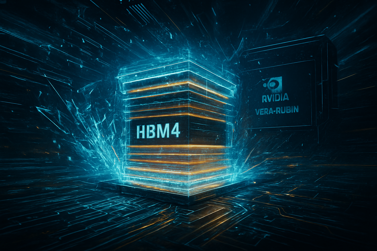
At the center of the storm is the formal introduction of the HBM4 standard, a revolutionary leap in memory technology designed to shatter the "memory wall" that has plagued AI scaling. As NVIDIA (NASDAQ: NVDA) prepares to launch its highly anticipated "Rubin" GPU architecture, the race to supply the necessary bandwidth has seen SK Hynix (KRX: 000660), Samsung Electronics (KRX: 005930), and Micron Technology (NASDAQ: MU) deploy their most aggressive technological roadmaps in history. The victor of this conflict will likely dictate the pace of AI development for the remainder of the decade.
Engineering the 16-Layer Titan
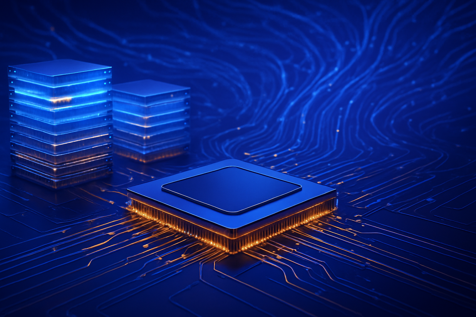
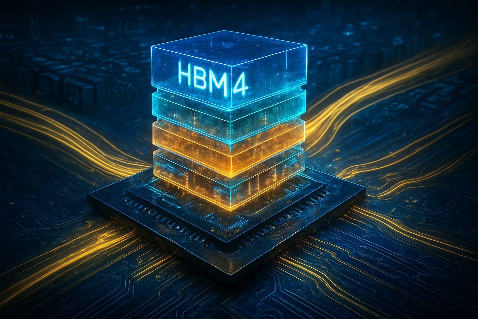
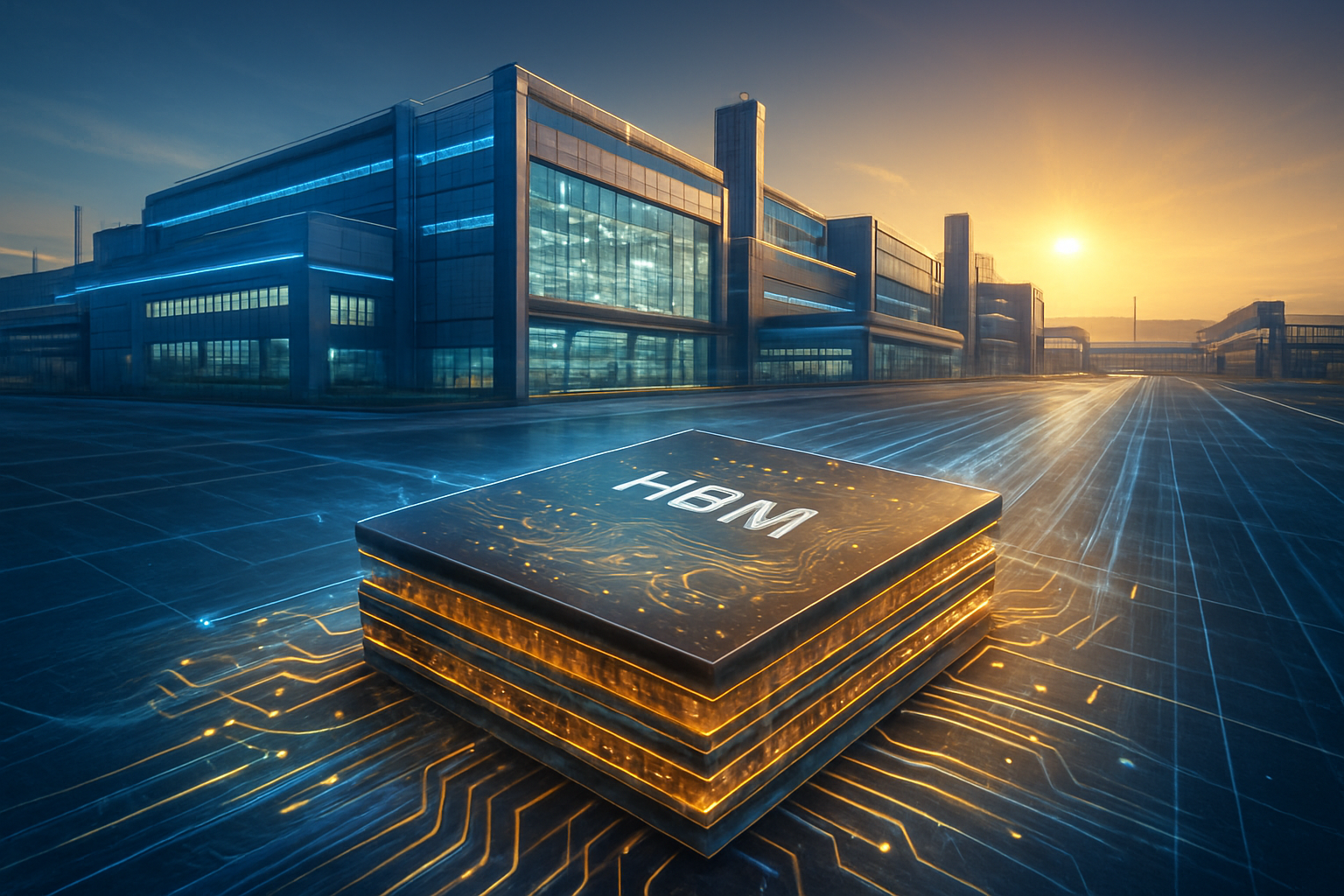
SK Hynix stole the spotlight at CES 2026 by demonstrating the world’s first 16-layer (16-Hi) HBM4 module, a massive 48GB stack that represents a nearly 50% increase in capacity over current HBM3E solutions. The technical centerpiece of this announcement is the implementation of a 2,048-bit interface—double the 1,024-bit width that has been the industry standard for a decade. By "widening the pipe" rather than simply increasing clock speeds, SK Hynix has achieved an unprecedented data throughput of 1.6 TB/s per stack, all while significantly reducing the power consumption and heat generation that have become major obstacles in modern data centers.
To achieve this 16-layer density, SK Hynix utilized its proprietary Advanced Mass Reflow Molded Underfill (MR-MUF) technology, thinning individual DRAM wafers to a staggering 30 micrometers—roughly the thickness of a human hair. This allows the company to stack 16 layers of high-density DRAM within the same physical height as previous 12-layer designs. Furthermore, the company highlighted a strategic alliance with TSMC (NYSE: TSM), using a specialized 12nm logic base die at the bottom of the stack. This collaboration allows for deeper integration between the memory and the processor, effectively turning the memory stack into a semi-intelligent co-processor that can handle basic data pre-processing tasks.
Initial reactions from the semiconductor research community have been overwhelmingly positive, though some experts caution about the manufacturing complexity. Dr. Elena Vos, Lead Architect at Silicon Analytics, noted that while the 2,048-bit interface is a "masterstroke of efficiency," the move toward hybrid bonding and extreme wafer thinning raises significant yield concerns. However, SK Hynix’s demonstration showed functional silicon running at 10 GT/s, suggesting that the company is much closer to mass production than its rivals might have hoped.
A Three-Way Clash for AI Dominance
While SK Hynix focused on density and interface width, Samsung Electronics counter-attacked with a focus on manufacturing efficiency and power. Samsung unveiled its HBM4 lineup based on its 1c nanometer process—the sixth generation of its 10nm-class DRAM. Samsung claims that this advanced node provides a 40% improvement in energy efficiency compared to competing 1b-based modules. In an era where NVIDIA's top-tier GPUs are pushing past 1,000 watts, Samsung is positioning its HBM4 as the only viable solution for sustainable, large-scale AI deployments. Samsung also signaled a massive production ramp-up at its Pyeongtaek facility, aiming to reach 250,000 wafers per month by the end of the year to meet the insatiable demand from hyperscalers.
Micron Technology, meanwhile, is leveraging its status as a highly efficient "third player" to disrupt the market. Micron used CES 2026 to announce that its entire HBM4 production capacity for the year has already been sold out through advance contracts. With a $20 billion capital expenditure plan and new manufacturing sites in Taiwan and Japan, Micron is banking on a "supply-first" strategy. While their early HBM4 modules focus on 12-layer stacks, they have promised a rapid transition to "HBM4E" by 2027, featuring 64GB capacities. This aggressive roadmap is clearly aimed at winning a larger share of the bill of materials for NVIDIA’s upcoming Rubin platform.
The primary beneficiary of this memory war is undoubtedly NVIDIA. The upcoming Rubin GPU is expected to utilize eight stacks of HBM4, providing a total of 384GB of high-speed memory and an aggregate bandwidth of 22 TB/s. This is nearly triple the bandwidth of the current Blackwell architecture, a requirement driven by the move toward "Reasoning Models" and Mixture-of-Experts (MoE) architectures that require massive amounts of data to be swapped in and out of the GPU memory at lightning speed.
Shattering the Memory Wall: The Strategic Stakes
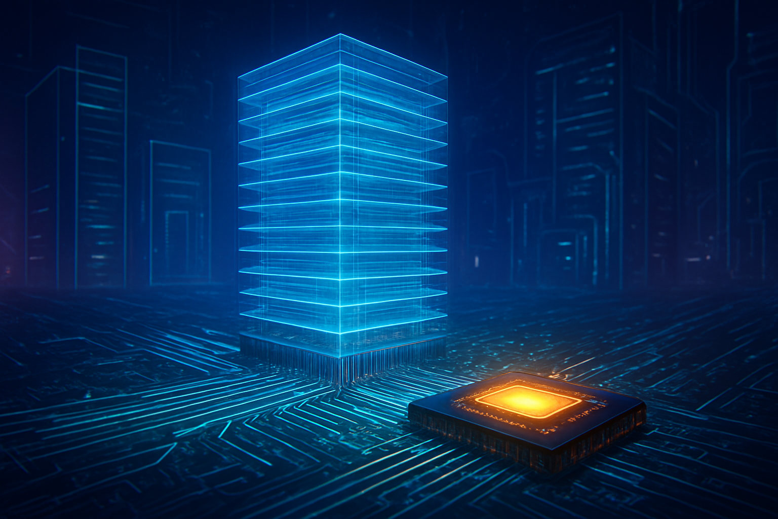
The significance of the HBM4 transition extends far beyond simple speed increases; it represents a fundamental shift in how computers are built. For decades, the "Von Neumann bottleneck"—the delay caused by the distance and speed limits between a processor and its memory—has limited computational performance. HBM4, with its 2,048-bit interface and logic-die integration, essentially fuses the memory and the processor together. This is the first time in history where memory is not just a storage bin, but a customized, active participant in the AI computation process.
This development is also a critical geopolitical and economic milestone. As nations race toward "Sovereign AI," the ability to secure a stable supply of high-performance memory has become a matter of national security. The massive capital requirements—running into the tens of billions of dollars for each company—ensure that the HBM market remains a highly exclusive club. This consolidation of power among SK Hynix, Samsung, and Micron creates a strategic choke point in the global AI supply chain, making these companies as influential as the foundries that print the AI chips themselves.
However, the "war" also brings concerns regarding the environmental footprint of AI. While HBM4 is more efficient per gigabyte of data transferred, the sheer scale of the units being deployed will lead to a net increase in data center power consumption. The shift toward 1,000-watt GPUs and multi-kilowatt server racks is forcing a total rethink of liquid cooling and power delivery infrastructure, creating a secondary market boom for cooling specialists and electrical equipment manufacturers.
The Horizon: Custom Logic and the Road to HBM5
Looking ahead, the next phase of the memory war will likely involve "Custom HBM." At CES 2026, both SK Hynix and Samsung hinted at future products where customers like Google or Amazon (NASDAQ: AMZN) could provide their own proprietary logic to be integrated directly into the HBM4 base die. This would allow for even more specialized AI acceleration, potentially moving functions like encryption, compression, and data search directly into the memory stack itself.
In the near term, the industry will be watching the "yield race" closely. Demonstrating a 16-layer stack at a trade show is one thing; consistently manufacturing them at the millions-per-month scale required by NVIDIA is another. Experts predict that the first half of 2026 will be defined by rigorous qualification tests, with the first Rubin-powered servers hitting the market late in the fourth quarter. Meanwhile, whisperings of HBM5 are already beginning, with early proposals suggesting another doubling of the interface or the move to 3D-integrated memory-on-logic architectures.
A Decisive Moment for the AI Hardware Stack
The CES 2026 HBM4 announcements represent a watershed moment in semiconductor history. We are witnessing the end of the "general purpose" memory era and the dawn of the "application-specific" memory age. SK Hynix’s 16-Hi breakthrough and Samsung’s 1c process efficiency are not just technical achievements; they are the enabling technologies that will determine whether AI can continue its exponential growth or if it will be throttled by hardware limitations.
As we move forward into 2026, the key indicators of success will be yield rates and the ability of these manufacturers to manage the thermal complexities of 3D stacking. The "Memory War" is far from over, but the opening salvos at CES have made one thing clear: the future of artificial intelligence is no longer just about the speed of the processor—it is about the width and depth of the memory that feeds it. Investors and tech leaders should watch for the first Rubin-HBM4 benchmark results in early Q3 for the next major signal of where the industry is headed.
This content is intended for informational purposes only and represents analysis of current AI developments.
TokenRing AI delivers enterprise-grade solutions for multi-agent AI workflow orchestration, AI-powered development tools, and seamless remote collaboration platforms.
For more information, visit https://www.tokenring.ai/.