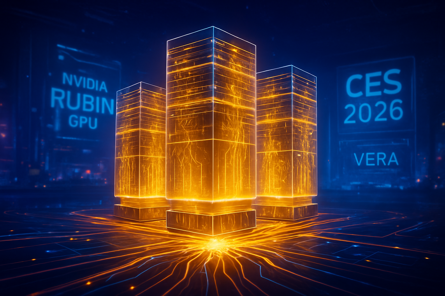
The 2026 Consumer Electronics Show (CES) in Las Vegas has transformed from a showcase of consumer gadgets into the primary battlefield for the most critical component in the artificial intelligence era: High Bandwidth Memory (HBM). As of January 8, 2026, the industry is witnessing the eruption of the "HBM4 Memory War," a high-stakes conflict between the world’s three largest memory manufacturers—SK Hynix (KRX: 000660), Samsung Electronics (KRX: 005930), and Micron Technology (NASDAQ: MU). This technological arms race is not merely about storage; it is a desperate sprint to provide the massive data throughput required by NVIDIA’s (NASDAQ: NVDA) newly detailed "Rubin" platform, the successor to the record-breaking Blackwell architecture.
The significance of this development cannot be overstated. As AI models grow to trillions of parameters, the bottleneck has shifted from raw compute power to memory bandwidth and energy efficiency. The announcements made this week at CES 2026 signal a fundamental shift in semiconductor architecture, where memory is no longer a passive storage bin but an active, logic-integrated component of the AI processor itself. With billions of dollars in capital expenditure on the line, the winners of this HBM4 cycle will likely dictate the pace of AI advancement for the remainder of the decade.
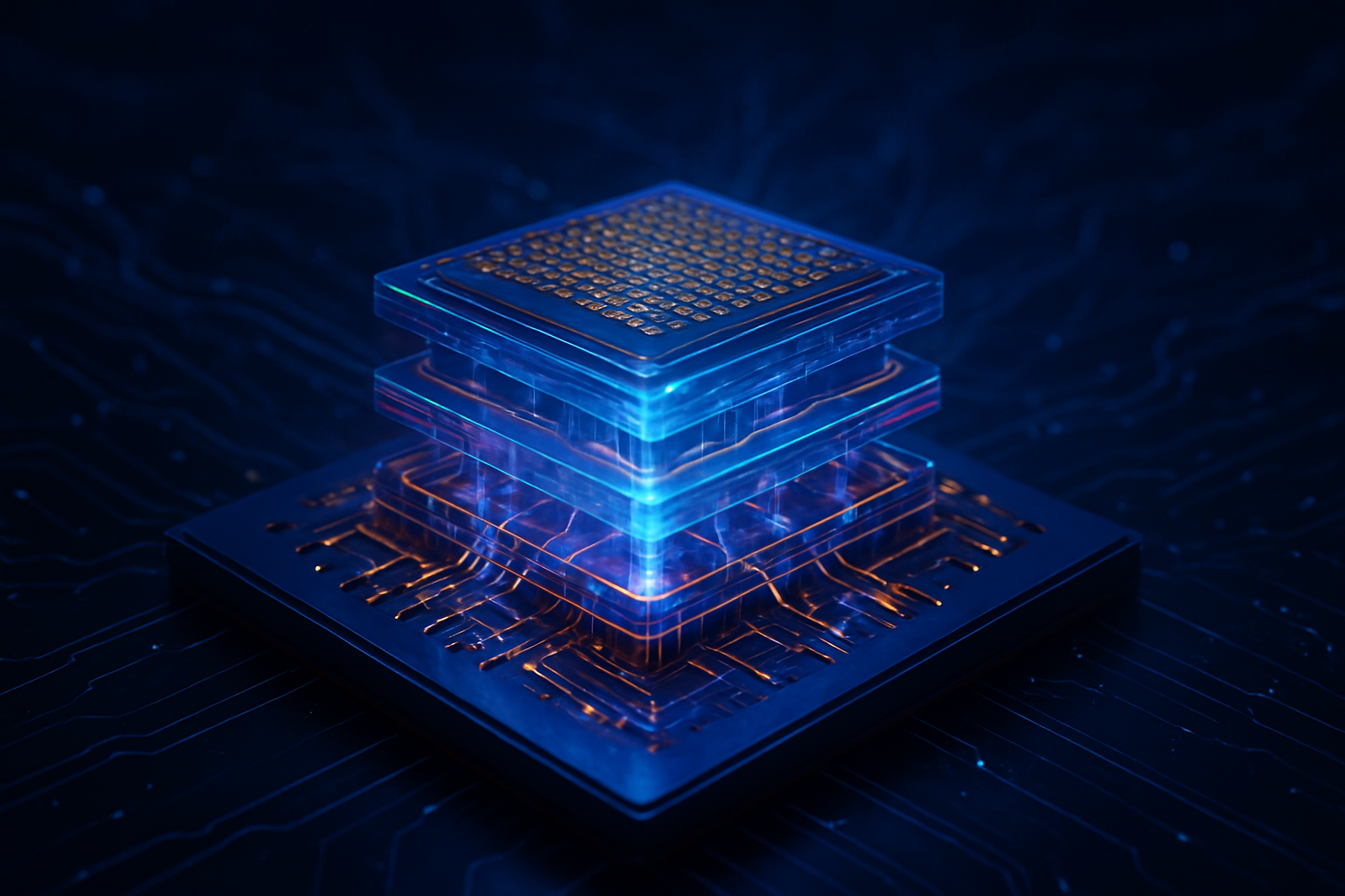
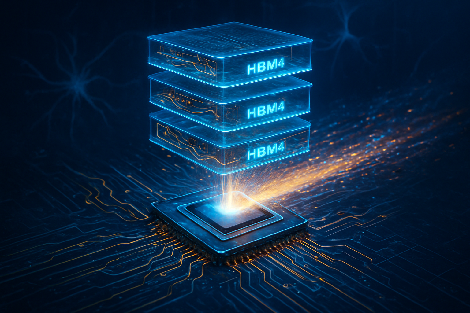
Technical Frontiers: 16-Layer Stacks and the 1c Process
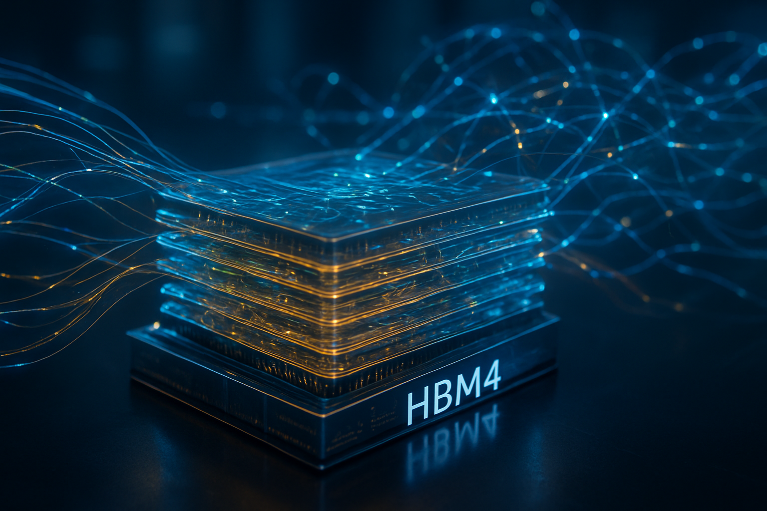
The technical specifications unveiled at CES 2026 represent a monumental leap over the previous HBM3E standard. SK Hynix stole the early headlines by debuting the world’s first 16-layer 48GB HBM4 module. To achieve this, the company utilized its proprietary Advanced Mass Reflow Molded Underfill (MR-MUF) technology, thinning individual DRAM wafers to a staggering 30 micrometers to fit within the strict 775µm height limit set by JEDEC. This 16-layer stack delivers an industry-leading data rate of 11.7 Gbps per pin, which, when integrated into an 8-stack system like NVIDIA’s Rubin, provides a system-level bandwidth of 22 TB/s—nearly triple that of early HBM3E systems.
Samsung Electronics countered with a focus on manufacturing sophistication and efficiency. Samsung’s HBM4 is built on its "1c" nanometer process (the 6th generation of 10nm-class DRAM). By moving to this advanced node, Samsung claims a 40% improvement in energy efficiency over its competitors. This is a critical advantage for data center operators struggling with the thermal demands of GPUs that now exceed 1,000 watts. Unlike its rivals, Samsung is leveraging its internal foundry to produce the HBM4 logic base die using a 10nm logic process, positioning itself as a "one-stop shop" that controls the entire stack from the silicon to the final packaging.
Micron Technology, meanwhile, showcased its aggressive capacity expansion and its role as a lead partner for the initial Rubin launch. Micron’s HBM4 entry focuses on a 12-high (12-Hi) 36GB stack that emphasizes a 2048-bit interface—double the width of HBM3E. This allows for speeds exceeding 2.0 TB/s per stack while maintaining a 20% power efficiency gain over previous generations. The industry reaction has been one of collective awe; experts from the AI research community note that the shift from memory-based nodes to logic nodes (like TSMC’s 5nm for the base die) effectively turns HBM4 into a "custom" memory solution that can be tailored for specific AI workloads.
The Kingmaker: NVIDIA’s Rubin Platform and the Supply Chain Scramble
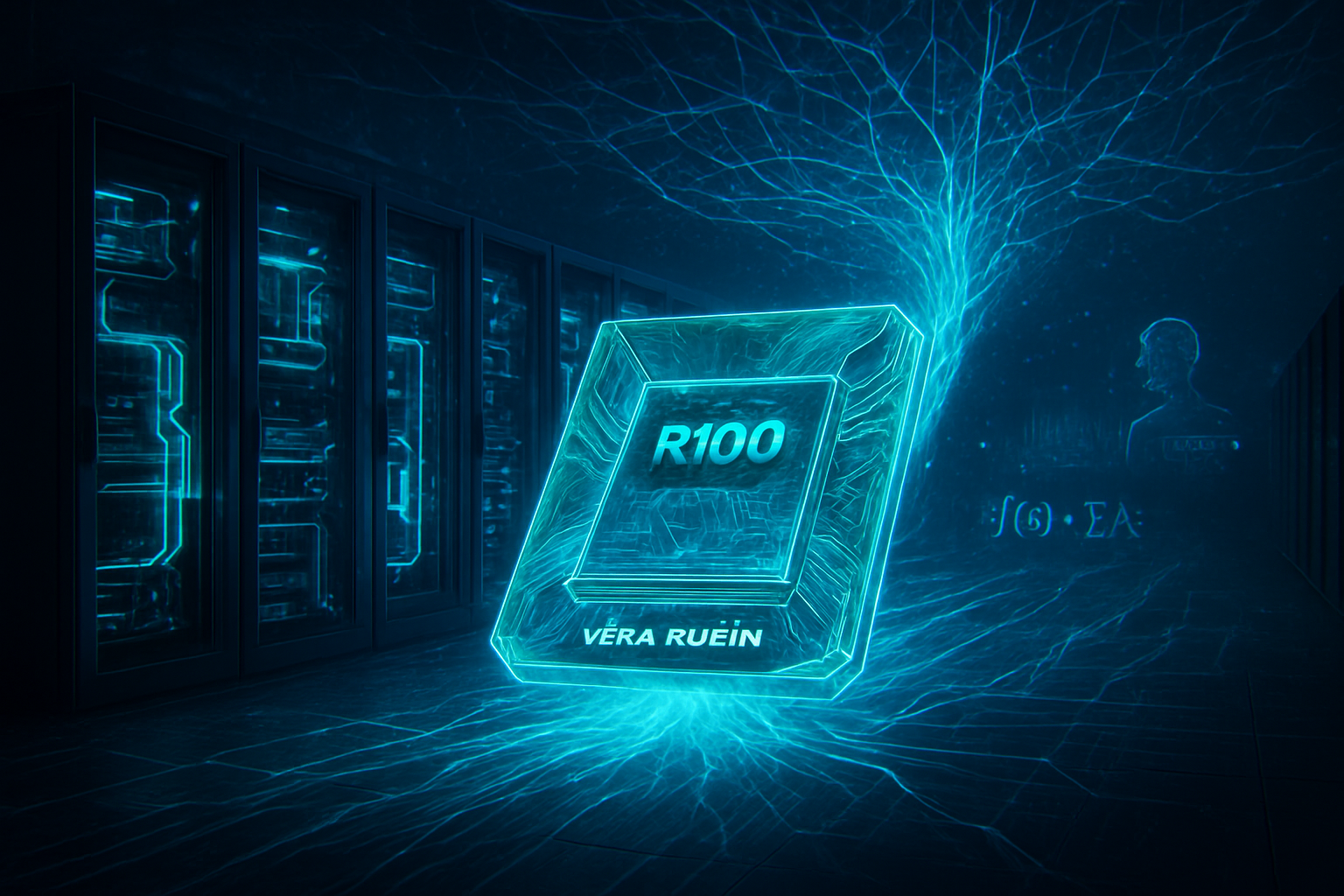
The primary driver of this memory frenzy is NVIDIA’s Rubin platform, which was the centerpiece of the CES 2026 keynote. The Rubin R100 and R200 GPUs, built on TSMC’s (NYSE: TSM) 3nm process, are designed to consume HBM4 at an unprecedented scale. Each Rubin GPU is expected to utilize eight stacks of HBM4, totaling 288GB of memory per chip. To ensure it does not repeat the supply shortages that plagued the Blackwell launch, NVIDIA has reportedly secured massive capacity commitments from all three major vendors, effectively acting as the kingmaker in the semiconductor market.
Micron has responded with the most aggressive capacity expansion in its history, targeting a dedicated HBM4 production capacity of 15,000 wafers per month by the end of 2026. This is part of a broader $20 billion capital expenditure plan that includes new facilities in Taiwan and a "megaplant" in Hiroshima, Japan. By securing such a large slice of the Rubin supply chain, Micron is moving from its traditional "third-place" position to a primary supplier status, directly challenging the dominance of SK Hynix.
The competitive implications extend beyond the memory makers. For AI labs and tech giants like Google (NASDAQ: GOOGL), Meta (NASDAQ: META), and Microsoft (NASDAQ: MSFT), the availability of HBM4-equipped Rubin GPUs will determine their ability to train next-generation "Agentic AI" models. Companies that can secure early allocations of these high-bandwidth systems will have a strategic advantage in inference speed and cost-per-query, potentially disrupting existing SaaS products that are currently limited by the latency of older hardware.
A Paradigm Shift: From Compute-Centric to Memory-Centric AI
The "HBM4 War" marks a broader shift in the AI landscape. For years, the industry focused on "Teraflops"—the number of floating-point operations a processor could perform. However, as models have grown, the energy cost of moving data between the processor and memory has become the primary constraint. The integration of logic dies into HBM4, particularly through the SK Hynix and TSMC "One-Team" alliance, signifies the end of the compute-only era. By embedding memory controllers and physical layer interfaces directly into the memory stack, manufacturers are reducing the physical distance data must travel, thereby slashing latency and power consumption.
This development also brings potential concerns regarding market consolidation. The technical complexity and capital requirements of HBM4 are so high that smaller players are being priced out of the market entirely. We are seeing a "triopoly" where SK Hynix, Samsung, and Micron hold all the cards. Furthermore, the reliance on advanced packaging techniques like Hybrid Bonding and MR-MUF creates a new set of manufacturing risks; any yield issues at these nanometer scales could lead to global shortages of AI hardware, stalling progress in fields from drug discovery to climate modeling.
Comparisons are already being drawn to the 2023 "GPU shortage," but with a twist. While 2023 was about the chips themselves, 2026 is about the interconnects and the stacking. The HBM4 breakthrough is arguably more significant than the jump from H100 to B100, as it addresses the fundamental "memory wall" that has threatened to plateau AI scaling laws.
The Horizon: Rubin Ultra and the Road to 1TB Per GPU
Looking ahead, the roadmap for HBM4 is already extending into 2027 and beyond. During the CES presentations, hints were dropped regarding the "Rubin Ultra" refresh, which is expected to move to 16-high HBM4e (Extended) stacks. This would effectively double the memory capacity again, potentially allowing for 1 terabyte of HBM memory on a single GPU package. Micron and SK Hynix are already sampling these 16-Hi stacks, with mass production targets set for early 2027.
The next major challenge will be the move to "Custom HBM" (cHBM), where AI companies like OpenAI or Tesla (NASDAQ: TSLA) may design their own proprietary logic dies to be manufactured by TSMC and then stacked with DRAM by SK Hynix or Micron. This level of vertical integration would allow for AI-specific optimizations that are currently impossible with off-the-shelf components. Experts predict that by 2028, the distinction between "processor" and "memory" will have blurred so much that we may begin referring to them as unified "AI Compute Cubes."
Final Reflections on the Memory-First Era
The events at CES 2026 have made one thing clear: the future of artificial intelligence is being written in the cleanrooms of memory fabs. SK Hynix’s 16-layer breakthrough, Samsung’s 1c process efficiency, and Micron’s massive capacity ramp-up for NVIDIA’s Rubin platform collectively represent a new chapter in semiconductor history. We have moved past the era of general-purpose computing into a period of extreme specialization, where the ability to move data is as important as the ability to process it.
As we move into the first quarter of 2026, the industry will be watching for the first production yields of these HBM4 modules. The success of the Rubin platform—and by extension, the next leap in AI capability—depends entirely on whether these three memory giants can deliver on their ambitious promises. For now, the "Memory War" is in full swing, and the spoils of victory are nothing less than the foundation of the global AI economy.
This content is intended for informational purposes only and represents analysis of current AI developments.
TokenRing AI delivers enterprise-grade solutions for multi-agent AI workflow orchestration, AI-powered development tools, and seamless remote collaboration platforms.
For more information, visit https://www.tokenring.ai/.