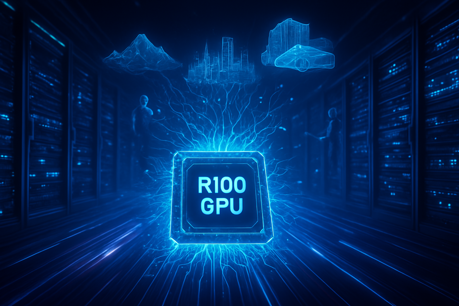
In a move that has sent shockwaves through the semiconductor industry, Advanced Micro Devices, Inc. (NASDAQ: AMD) has officially unveiled its most ambitious AI infrastructure to date: the Instinct MI450 accelerator and the integrated Helios server rack platform. Positioned as a direct assault on the high-end generative AI market, the MI450 is the first GPU to break the 400GB memory barrier, sporting a massive 432GB of next-generation HBM4 memory. This announcement marks a definitive shift in the AI hardware wars, as AMD moves from being a fast-follower to a pioneer in memory-centric compute architecture.
The immediate significance of the Helios platform cannot be overstated. By delivering an unprecedented 2.9 ExaFLOPS of FP4 performance in a single rack, AMD is providing the raw horsepower necessary to train the next generation of multi-trillion parameter models. More importantly, the partnership with Meta Platforms, Inc. (NASDAQ: META) to standardize this hardware under the Open Rack Wide (ORW) initiative signals a transition away from proprietary, vertically integrated systems toward an open, interoperable ecosystem. With early commitments from Oracle Corporation (NYSE: ORCL) and OpenAI, the MI450 is poised to become the foundational layer for the world’s most advanced AI services.
The Technical Deep-Dive: CDNA 5 and the 432GB Memory Frontier
At the heart of the MI450 lies the new CDNA 5 architecture, manufactured on TSMC’s cutting-edge 2nm process node. The most striking specification is the 432GB of HBM4 memory per GPU, which provides nearly 20 TB/s of memory bandwidth. This massive capacity is designed to solve the "memory wall" that has plagued AI scaling, allowing researchers to fit significantly larger model shards or massive KV caches for long-context inference directly into the GPU’s local memory. By comparison, this is nearly double the capacity of current-generation hardware, drastically reducing the need for complex and slow off-chip data movement.
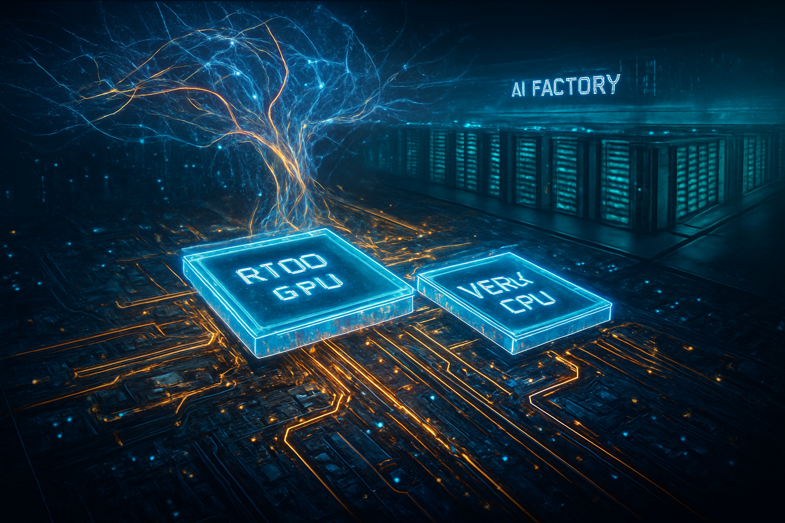
The Helios server rack serves as the delivery vehicle for this power, integrating 72 MI450 GPUs with AMD’s latest "Venice" EPYC CPUs. The rack's performance is staggering, reaching 2.9 ExaFLOPS of FP4 compute and 1.45 ExaFLOPS of FP8. To manage the massive heat generated by these 1,500W chips, the Helios rack utilizes a fully liquid-cooled design optimized for the 120kW+ power densities common in modern hyperscale data centers. This is not just a collection of chips; it is a highly tuned "AI supercomputer in a box."
AMD has also doubled down on interconnect technology. Helios utilizes the Ultra Accelerator Link (UALink) for internal GPU-to-GPU communication, offering 260 TB/s of aggregate bandwidth. For scaling across multiple racks, AMD employs the Ultra Ethernet Consortium (UEC) standard via its "Vulcano" DPUs. This commitment to open standards is a direct response to the proprietary NVLink technology used by NVIDIA Corporation (NASDAQ: NVDA), offering customers a path to build massive clusters without being locked into a single vendor's networking stack.
Industry experts have reacted with cautious optimism, noting that while the hardware specs are industry-leading, the success of the MI450 will depend heavily on the maturity of AMD’s ROCm software stack. However, early benchmarks shared by OpenAI suggest that the software-hardware integration has reached a "tipping point," where the performance-per-watt and memory advantages of the MI450 now rival or exceed the best offerings from the competition in specific large-scale training workloads.
Market Implications: A New Contender for the AI Throne
The launch of the MI450 and Helios platform creates a significant competitive threat to NVIDIA’s market dominance. While NVIDIA’s Blackwell and upcoming Rubin systems remain the gold standard for many, AMD’s focus on massive memory capacity and open standards appeals to hyperscalers like Meta and Oracle who are wary of vendor lock-in. By adopting the Open Rack Wide (ORW) standard, Meta is ensuring that its future data centers can seamlessly integrate AMD hardware alongside other OCP-compliant components, potentially driving down total cost of ownership (TCO) across its global infrastructure.
Oracle has already moved to capitalize on this, announcing plans to deploy 50,000 MI450 GPUs within its Oracle Cloud Infrastructure (OCI) starting in late 2026. This move positions Oracle as a premier destination for AI startups looking for the highest possible memory capacity at a competitive price point. Similarly, OpenAI’s strategic pivot to include AMD in its 1-gigawatt compute expansion plan suggests that even the most advanced AI labs are looking to diversify their hardware portfolios to ensure supply chain resilience and leverage AMD’s unique architectural advantages.
For hardware partners like Hewlett Packard Enterprise (NYSE: HPE) and Super Micro Computer, Inc. (NASDAQ: SMCI), the Helios platform provides a standardized reference design that can be rapidly brought to market. This "turnkey" approach allows these OEMs to offer high-performance AI clusters to enterprise customers who may not have the engineering resources of a Meta or Microsoft but still require exascale-class compute. The disruption to the market is clear: NVIDIA no longer has a monopoly on the high-end AI "pod" or "rack" solution.
The strategic advantage for AMD lies in its ability to offer a "memory-first" architecture. As models continue to grow in size and complexity, the ability to store more parameters on-chip becomes a decisive factor in both training speed and inference latency. By leading the transition to HBM4 with such a massive capacity jump, AMD is betting that the industry's bottleneck will remain memory, not just raw compute cycles—a bet that seems increasingly likely to pay off.
The Wider Significance: Exascale for the Masses and the Open Standard Era
The MI450 and Helios announcement represents a broader trend in the AI landscape: the democratization of exascale computing. Only a few years ago, "ExaFLOPS" was a term reserved for the world’s largest national supercomputers. Today, AMD is promising nearly 3 ExaFLOPS in a single, albeit large, server rack. This compression of compute power is what will enable the transition from today’s large language models to future "World Models" that require massive multimodal processing and real-time reasoning capabilities.
Furthermore, the partnership between AMD and Meta on the ORW standard marks a pivotal moment for the Open Compute Project (OCP). It signals that the era of "black box" AI hardware may be coming to an end. As power requirements for AI racks soar toward 150kW and beyond, the industry requires standardized cooling, power delivery, and physical dimensions to ensure that data centers can remain flexible. AMD’s willingness to "open source" the Helios design through the OCP ensures that the entire industry can benefit from these architectural innovations.
However, this leap in performance does not come without concerns. The 1,500W TGP of the MI450 and the 120kW+ power draw of a single Helios rack highlight the escalating energy demands of the AI revolution. Critics point out that the environmental impact of such systems is immense, and the pressure on local power grids will only increase as these racks are deployed by the thousands. AMD’s focus on FP4 performance is partly an effort to address this, as lower-precision math can provide significant efficiency gains, but the absolute power requirements remain a daunting challenge.
In the context of AI history, the MI450 launch may be remembered as the moment when the "memory wall" was finally breached. Much like the transition from CPUs to GPUs for deep learning a decade ago, the shift to massive-capacity HBM4 systems marks a new phase of hardware optimization where data locality is the primary driver of performance. It is a milestone that moves the industry closer to the goal of "Artificial General Intelligence" by providing the necessary hardware substrate for models that are orders of magnitude more complex than what we see today.
Looking Ahead: The Road to 2027 and Beyond
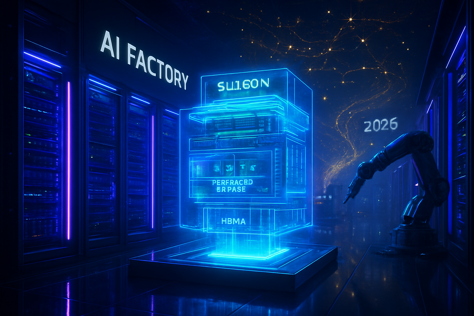
The near-term roadmap for AMD involves a rigorous rollout schedule, with initial Helios units shipping to key partners like Oracle and OpenAI throughout late 2026. The real test will be the "Day 1" performance of these systems in a production environment. Developers will be watching closely to see if the ROCm 7.0 software suite can provide the seamless "drop-in" compatibility with PyTorch and JAX that has been promised. If AMD can prove that the software friction is gone, the floodgates for MI450 adoption will likely open.
Looking further out, the competition will only intensify. NVIDIA’s Rubin platform is expected to respond with even higher peak compute figures, potentially reclaiming the FLOPS lead. However, rumors suggest AMD is already working on an "MI450X" refresh that could push memory capacity even higher or introduce 3D-stacked cache technologies to further reduce latency. The battle for 2027 will likely center on "agentic" AI workloads, which require high-speed, low-latency inference that plays directly into the MI450’s strengths.
The ultimate challenge for AMD will be maintaining this pace of innovation while managing the complexities of 2nm manufacturing and the global supply chain for HBM4. As demand for AI compute continues to outstrip supply, the company that can not only design the best chip but also manufacture and deliver it at scale will win. With the MI450 and Helios, AMD has proven it has the design; now, it must prove it has the execution to match.
Conclusion: A Generational Shift in AI Infrastructure
The unveiling of the AMD Instinct MI450 and the Helios platform represents a landmark achievement in semiconductor engineering. By delivering 432GB of HBM4 memory and 2.9 ExaFLOPS of performance, AMD has provided a compelling alternative to the status quo, grounded in open standards and industry-leading memory capacity. This is more than just a product launch; it is a declaration of intent that AMD intends to lead the next decade of AI infrastructure.
The significance of this development lies in its potential to accelerate the development of more capable, more efficient AI models. By breaking the memory bottleneck and embracing open architectures, AMD is fostering an environment where innovation can happen at the speed of software, not just the speed of hardware cycles. The early adoption by industry giants like Meta, Oracle, and OpenAI is a testament to the fact that the market is ready for a multi-vendor AI future.
In the coming weeks and months, all eyes will be on the initial deployment benchmarks and the continued evolution of the UALink and UEC ecosystems. As the first Helios racks begin to hum in data centers across the globe, the AI industry will enter a new era of competition—one that promises to push the boundaries of what is possible and bring us one step closer to the next frontier of artificial intelligence.
This content is intended for informational purposes only and represents analysis of current AI developments.
TokenRing AI delivers enterprise-grade solutions for multi-agent AI workflow orchestration, AI-powered development tools, and seamless remote collaboration platforms.
For more information, visit https://www.tokenring.ai/.