The global race for semiconductor supremacy has reached a fever pitch as the calendar turns to 2026. In a move that signals the imminent arrival of the next generation of artificial intelligence, both Samsung Electronics (KRX: 005930) and SK Hynix (KRX: 000660) have officially transitioned from prototyping to the delivery of paid final samples of 6th-generation High Bandwidth Memory (HBM4) to NVIDIA (NASDAQ: NVDA). These samples are currently undergoing final quality verification for integration into NVIDIA’s highly anticipated 'Rubin' R100 GPUs, marking the start of a new era in AI hardware capability.
The delivery of paid samples is a critical milestone, indicating that the technology has matured beyond experimental stages and is meeting the rigorous performance and reliability standards required for mass-market data center deployment. As NVIDIA prepares to roll out the Rubin architecture in early 2026, the battle between the world’s leading memory makers is no longer just about who can produce the fastest chips, but who can manufacture them at the unprecedented scale required by the "AI arms race."
Technical Breakthroughs: Doubling the Data Highway
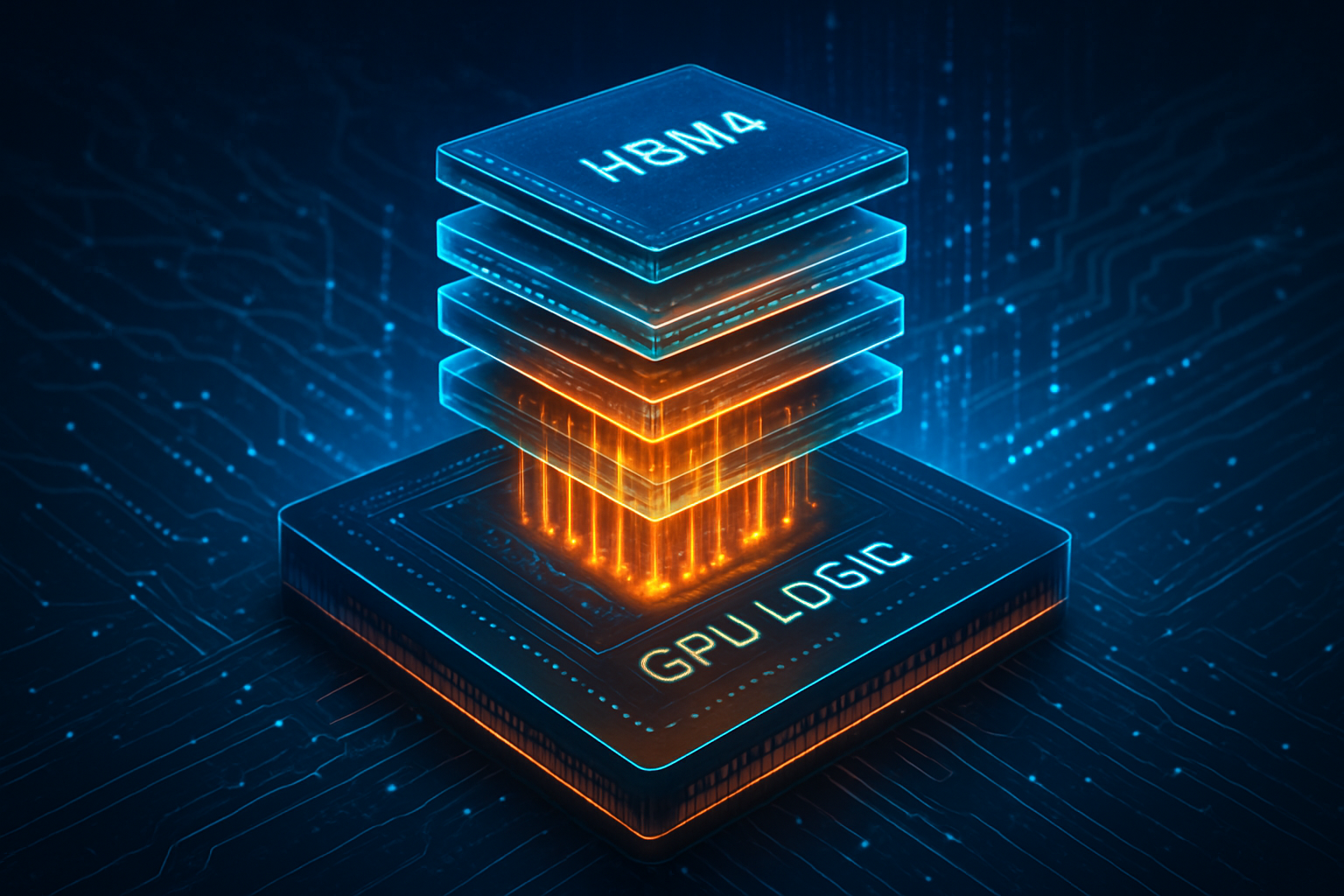
The transition from HBM3e to HBM4 represents the most significant architectural shift in the history of high-bandwidth memory. While previous generations focused on incremental speed increases, HBM4 fundamentally redesigns the interface between the memory and the processor. The most striking change is the doubling of the data bus width from 1,024-bit to a massive 2,048-bit interface. This "wider road" allows for a staggering increase in data throughput without the thermal and power penalties associated with simply increasing clock speeds.
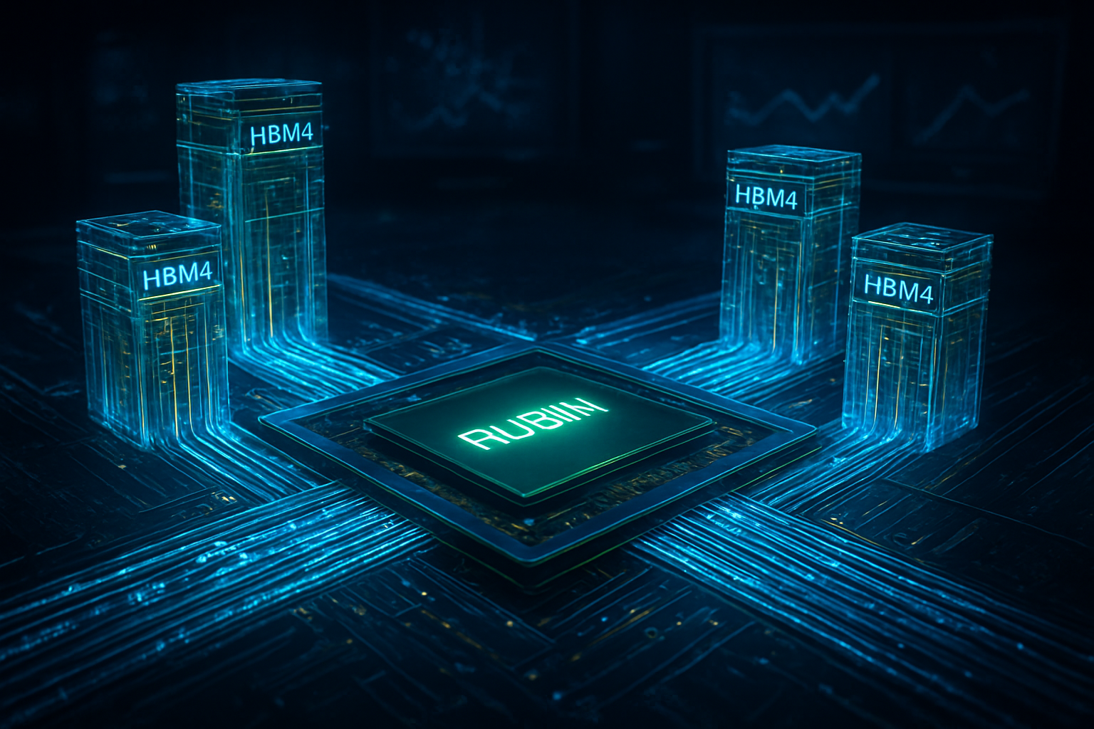
NVIDIA’s Rubin R100 GPU, the primary beneficiary of this advancement, is expected to be a powerhouse of efficiency and performance. Built on TSMC (NYSE: TSM)’s advanced N3P (3nm) process, the Rubin architecture utilizes a chiplet-based design that incorporates eight HBM4 stacks. This configuration provides a total of 288GB of VRAM and a peak bandwidth of 13 TB/s—a 60% increase over the current Blackwell B100. Furthermore, HBM4 introduces 16-layer stacking (16-Hi), allowing for higher density and capacity per stack, which is essential for the trillion-parameter models that are becoming the industry standard.
The industry has also seen a shift in how these chips are built. SK Hynix has formed a "One-Team" alliance with TSMC to manufacture the HBM4 logic base die using TSMC’s logic processes, rather than traditional memory processes. This allows for tighter integration and lower latency. Conversely, Samsung is touting its "turnkey" advantage, using its own 4nm foundry to produce the base die, memory cells, and advanced packaging in-house. Initial reactions from the research community suggest that this diversification of manufacturing approaches is critical for stabilizing the global supply chain as demand continues to outstrip supply.
Shifting the Competitive Landscape
The HBM4 rollout is poised to reshape the hierarchy of the semiconductor industry. For Samsung, this is a "redemption arc" moment. After trailing SK Hynix during the HBM3e cycle, Samsung is planning a massive 50% surge in HBM production capacity by 2026, aiming for a monthly output of 250,000 wafers. By leveraging its vertically integrated structure, Samsung hopes to recapture its position as the world’s leading memory supplier and secure a larger share of NVIDIA’s lucrative contracts.
SK Hynix, however, is not yielding its lead easily. As the incumbent preferred supplier for NVIDIA, SK Hynix has already established a mass production system at its M16 and M15X fabs, with full-scale manufacturing slated to begin in February 2026. The company’s deep technical partnership with NVIDIA and TSMC gives it a strategic advantage in optimizing memory for the Rubin architecture. Meanwhile, Micron Technology (NASDAQ: MU) remains a formidable third player, focusing on high-efficiency HBM4 designs that target the growing market for edge AI and specialized accelerators.
For NVIDIA, the availability of HBM4 from multiple reliable sources is a strategic win. It reduces reliance on a single supplier and provides the necessary components to maintain its yearly release cycle. The competition between Samsung and SK Hynix also exerts downward pressure on costs and accelerates the pace of innovation, ensuring that NVIDIA remains the undisputed leader in AI training and inference hardware.
Breaking the "Memory Wall" and the Future of AI
The broader significance of the HBM4 transition lies in its ability to address the "Memory Wall"—the growing bottleneck where processor performance outpaces the ability of memory to feed it data. As AI models move toward 10-trillion and 100-trillion parameters, the sheer volume of data that must be moved between the GPU and memory becomes the primary limiting factor in performance. HBM4’s 13 TB/s bandwidth is not just a luxury; it is a necessity for the next generation of multimodal AI that can process video, voice, and text simultaneously in real-time.
Energy efficiency is another critical factor. Data centers are increasingly constrained by power availability and cooling requirements. By doubling the interface width, HBM4 can achieve higher throughput at lower clock speeds, reducing the energy cost per bit by approximately 40%. This efficiency gain is vital for the sustainability of gigawatt-scale AI clusters and helps cloud providers manage the soaring operational costs of AI infrastructure.
This milestone mirrors previous breakthroughs like the transition to DDR memory or the introduction of the first HBM chips, but the stakes are significantly higher. The ability to supply HBM4 has become a matter of national economic security for South Korea and a cornerstone of the global AI economy. As the industry moves toward 2026, the successful integration of HBM4 into the Rubin platform will likely be remembered as the moment when AI hardware finally caught up to the ambitions of AI software.
The Road Ahead: Customization and HBM4e
Looking toward the near future, the HBM4 era will be defined by customization. Unlike previous generations that were "off-the-shelf" components, HBM4 allows for the integration of custom logic dies. This means that AI companies can potentially request specific features to be baked directly into the memory stack, such as specialized encryption or data compression, further blurring the lines between memory and processing.
Experts predict that once the initial Rubin rollout is complete, the focus will quickly shift to HBM4e (Extended), which is expected to appear around late 2026 or early 2027. This iteration will likely push stacking to 20 or 24 layers, providing even greater density for the massive "sovereign AI" projects being undertaken by nations around the world. The primary challenge remains yield rates; as the complexity of 16-layer stacks and hybrid bonding increases, maintaining high production yields will be the ultimate test for Samsung and SK Hynix.
A New Benchmark for AI Infrastructure
The delivery of paid HBM4 samples to NVIDIA marks a definitive turning point in the AI hardware narrative. It signals that the industry is ready to support the next leap in artificial intelligence, providing the raw data-handling power required for the world’s most complex neural networks. The fierce competition between Samsung and SK Hynix has accelerated this timeline, ensuring that the Rubin architecture will launch with the most advanced memory technology ever created.
As we move into 2026, the key metrics to watch will be the yield rates of these 16-layer stacks and the performance benchmarks of the first Rubin-powered clusters. This development is more than just a technical upgrade; it is the foundation upon which the next generation of AI breakthroughs—from autonomous scientific discovery to truly conversational agents—will be built. The HBM4 race has only just begun, and the implications for the global tech landscape will be felt for years to come.
This content is intended for informational purposes only and represents analysis of current AI developments.
TokenRing AI delivers enterprise-grade solutions for multi-agent AI workflow orchestration, AI-powered development tools, and seamless remote collaboration platforms.
For more information, visit https://www.tokenring.ai/.