Tag: HBM4

  • The Trillion-Dollar Threshold: How the ‘AI Supercycle’ is Rewriting the Semiconductor Playbook

    The Trillion-Dollar Threshold: How the ‘AI Supercycle’ is Rewriting the Semiconductor Playbook

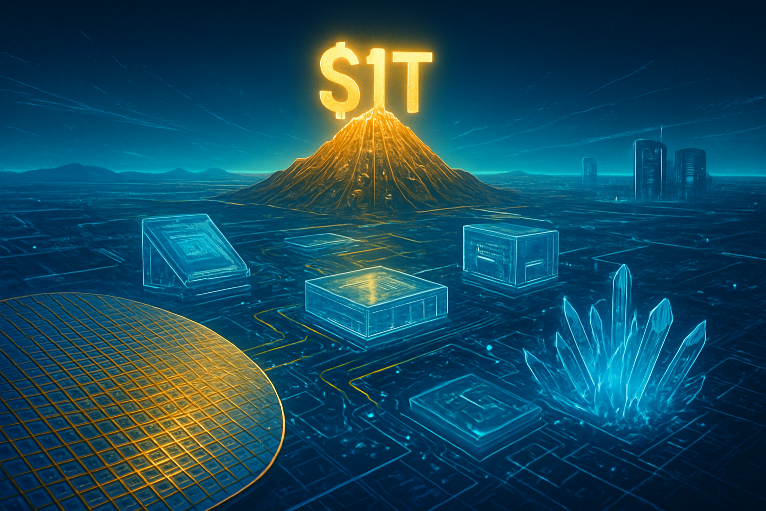
    As 2025 draws to a close, the global semiconductor industry is no longer just a cyclical component of the tech sector—it has become the foundational engine of the global economy. According to the World Semiconductor Trade Statistics (WSTS) Autumn 2025 forecast, the industry is on a trajectory to reach a staggering $975.5 billion in revenue by 2026, a 26.3% year-over-year increase that places the historic $1 trillion milestone within reach. This explosive growth is being fueled by what analysts have dubbed the "AI Supercycle," a structural shift driven by the transition from generative chatbots to autonomous AI agents that demand unprecedented levels of compute and memory.

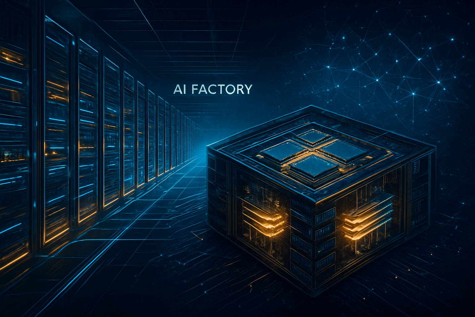
    The significance of this milestone cannot be overstated. For decades, the chip industry was defined by the "boom-bust" cycles of PCs and smartphones. However, the current expansion is different. With hyperscale capital expenditure from giants like Microsoft (NASDAQ: MSFT) and Alphabet (NASDAQ: GOOGL) projected to exceed $600 billion in 2026, the demand for high-performance logic and specialized memory is decoupling from traditional consumer electronics trends. We are witnessing the birth of the "AI Factory" era, where silicon is the new oil and compute capacity is the ultimate measure of national and corporate power.

    The Dawn of the Rubin Era and the HBM4 Revolution

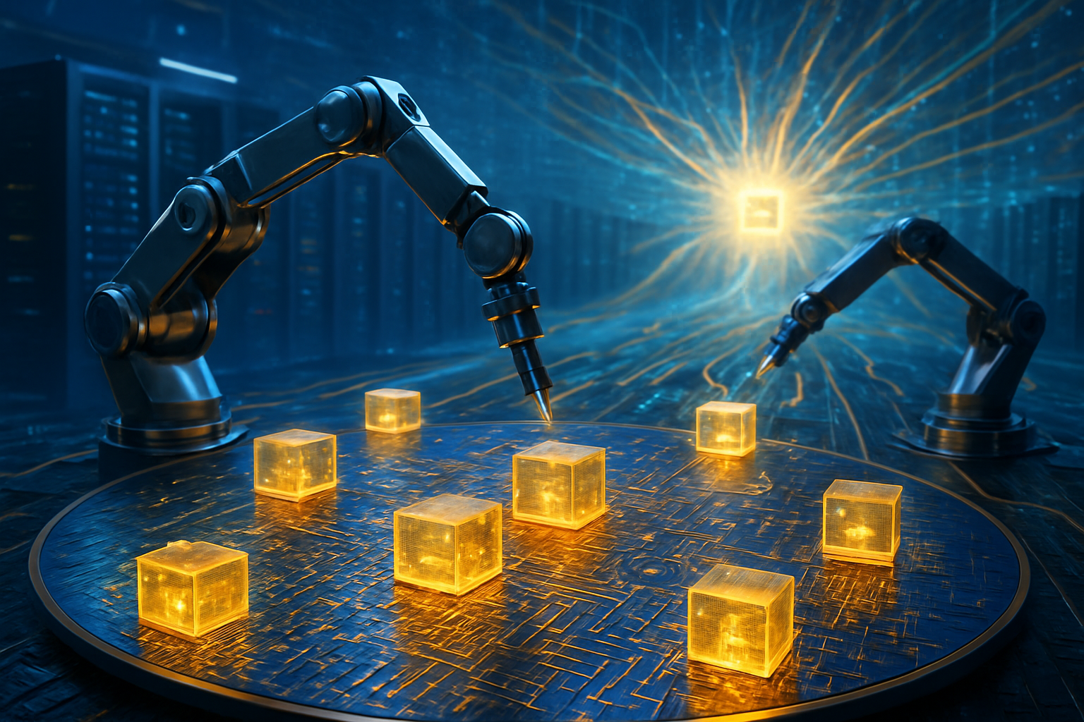
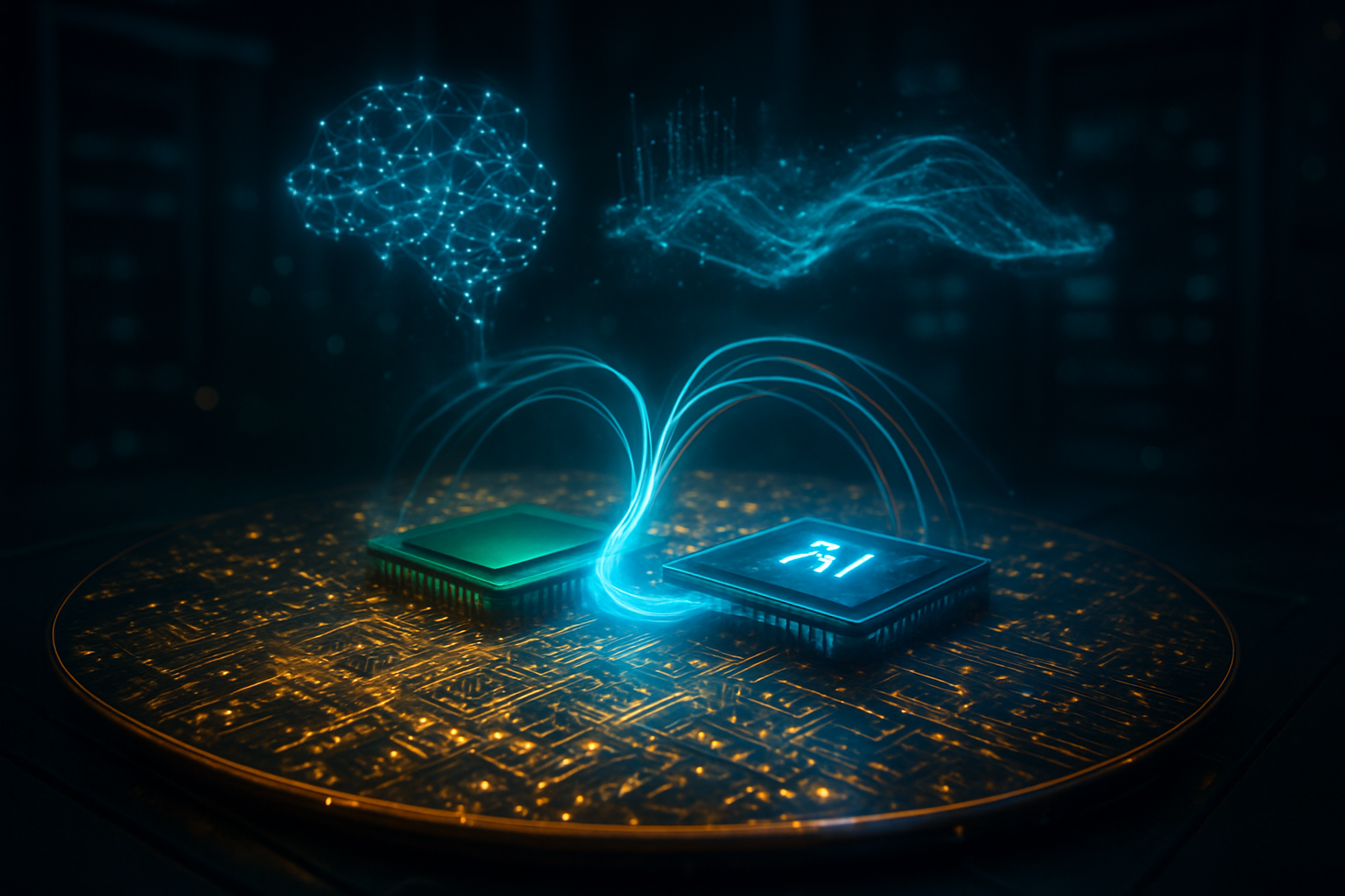
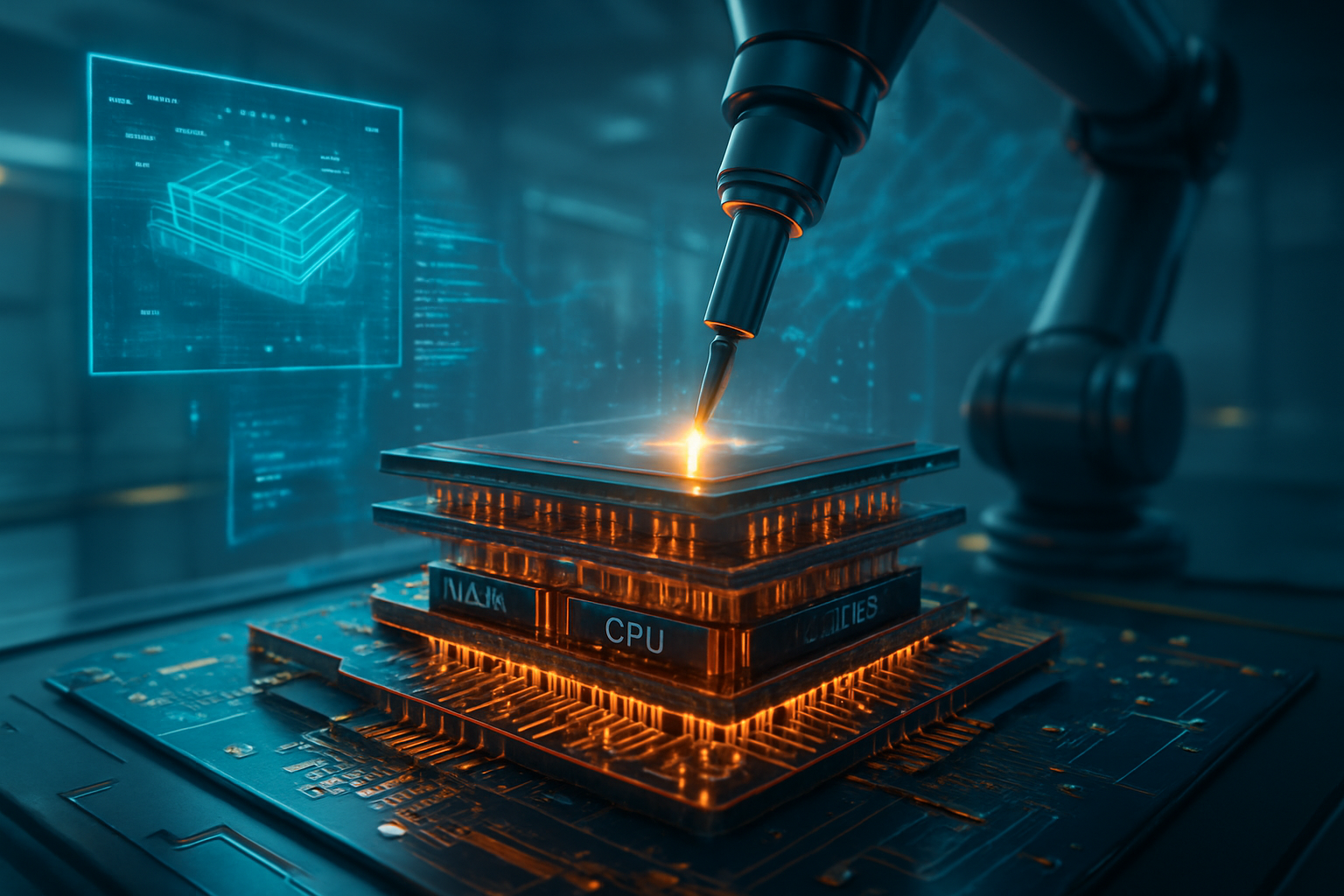
    Technically, the industry is entering its most ambitious phase yet. As of December 2024, NVIDIA (NASDAQ: NVDA) has successfully moved beyond its Blackwell architecture, with the first silicon for the Rubin platform having already taped out at TSMC (NYSE: TSM). Unlike previous generations, Rubin is a chiplet-based architecture designed specifically for the "Year of the Agent" in 2026. It integrates the new Vera CPU—featuring 88 custom ARM cores—and introduces the NVLink 6 interconnect, which doubles rack-scale bandwidth to a massive 260 TB/s.

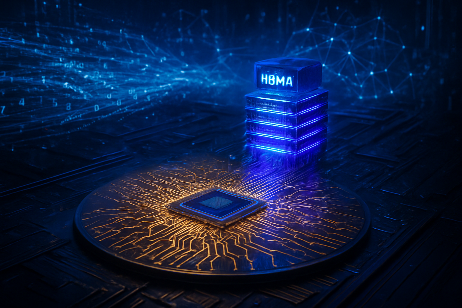
    Complementing these logic gains is a radical shift in memory architecture. The industry is currently validating HBM4 (High-Bandwidth Memory 4), which doubles the physical interface width from 1024-bit to 2048-bit. This jump allows for bandwidth exceeding 2.0 TB/s per stack, a necessity for the massive parameter counts of next-generation agentic models. Furthermore, TSMC is officially beginning mass production of its 2nm (N2) node this month. Utilizing Gate-All-Around (GAA) nanosheet transistors for the first time, the N2 node offers a 30% power reduction over the previous 3nm generation—a critical metric as data centers struggle with escalating energy costs.

    Strategic Realignment: The Winners of the Supercycle

    The business landscape is being reshaped by those who can master the "memory-to-compute" ratio. SK Hynix (KRX: 000660) continues to lead the HBM market with a projected 50% share for 2026, leveraging its advanced MR-MUF packaging technology. However, Samsung (KRX: 005930) is mounting a significant challenge with its "turnkey" strategy, offering a one-stop-shop for HBM4 logic dies and foundry services to regain the favor of major AI chip designers. Meanwhile, Micron (NASDAQ: MU) has already announced that its entire 2026 HBM production capacity is "sold out" via long-term supply agreements, highlighting the desperation for supply among hyperscalers.

    For the "Big Five" tech giants, the strategic advantage has shifted toward custom silicon. Amazon (NASDAQ: AMZN) and Meta (NASDAQ: META) are increasingly deploying their own AI inference chips (Trainium and MTIA, respectively) to reduce their multi-billion dollar reliance on external vendors. This "internalization" of the supply chain is creating a two-tiered market: high-end training remains dominated by NVIDIA’s Rubin and Blackwell, while specialized inference is becoming a battleground for custom ASICs and ARM-based architectures.

    Sovereign AI and the Global Energy Crisis

    Beyond the balance sheets, the AI Supercycle is triggering a geopolitical and environmental reckoning. "Sovereign AI" has emerged as a dominant trend in late 2025, with nations like Saudi Arabia and the UAE treating compute capacity as a strategic national asset. This "Compute Sovereignty" movement is driving massive localized infrastructure projects, as countries seek to build domestic LLMs to ensure they are not merely "technological vassals" to US-based providers.

    However, this growth is colliding with the physical limits of power grids. The projected electricity demand for AI data centers is expected to double by 2030, reaching levels equivalent to the total consumption of Japan. This has led to an unlikely alliance between Big Tech and nuclear energy. Microsoft and Amazon have recently signed landmark deals to restart decommissioned nuclear reactors and invest in Small Modular Reactors (SMRs). In 2026, the success of a chip company may depend as much on its energy efficiency as its raw TFLOPS performance.

    The Road to 1.4nm and Photonic Computing

    Looking ahead to 2026 and 2027, the roadmap enters the "Angstrom Era." Intel (NASDAQ: INTC) is racing to be the first to deploy High-NA EUV lithography for its 14A (1.4nm) node, a move that could determine whether the company can reclaim its manufacturing crown from TSMC. Simultaneously, the industry is pivoting toward photonic computing to break the "interconnect bottleneck." By late 2026, we expect to see the first mainstream adoption of Co-Packaged Optics (CPO), using light instead of electricity to move data between GPUs, potentially reducing interconnect power consumption by 30%.

    The challenges remain daunting. The "compute divide" between nations that can afford these $100 billion clusters and those that cannot is widening. Additionally, the shift toward agentic AI—where AI systems can autonomously execute complex workflows—requires a level of reliability and low-latency processing that current edge infrastructure is only beginning to support.

    Final Thoughts: A New Era of Silicon Hegemony

    The semiconductor industry’s approach to the $1 trillion revenue milestone is more than just a financial achievement; it is a testament to the fact that silicon has become the primary driver of global productivity. As we move into 2026, the "AI Supercycle" will continue to force a radical convergence of energy policy, national security, and advanced physics.

    The key takeaways for the coming months are clear: watch the yield rates of TSMC’s 2nm production, the speed of the nuclear-to-data-center integration, and the first real-world benchmarks of NVIDIA’s Rubin architecture. We are no longer just building chips; we are building the cognitive infrastructure of the 21st century.


    This content is intended for informational purposes only and represents analysis of current AI developments.

    TokenRing AI delivers enterprise-grade solutions for multi-agent AI workflow orchestration, AI-powered development tools, and seamless remote collaboration platforms.
    For more information, visit https://www.tokenring.ai/.

  • The HBM Gold Rush: Samsung and SK Hynix Pivot to HBM4 as Prices Soar

    The HBM Gold Rush: Samsung and SK Hynix Pivot to HBM4 as Prices Soar

    As 2025 draws to a close, the semiconductor landscape has been fundamentally reshaped by an insatiable hunger for artificial intelligence. What began as a surge in demand for GPUs has evolved into a full-scale "Gold Rush" for High-Bandwidth Memory (HBM), the critical silicon that feeds data to AI accelerators. Industry giants Samsung Electronics (KRX: 005930) and SK Hynix (KRX: 000660) are reporting record-breaking profit margins, fueled by a strategic pivot that is draining the supply of traditional DRAM to prioritize the high-margin HBM stacks required by the next generation of AI data centers.

    This week, as the industry looks toward 2026, the transition to the HBM4 standard has reached a fever pitch. With NVIDIA (NASDAQ: NVDA) preparing its upcoming "Rubin" architecture, the world’s leading memory makers are locked in a high-stakes race to qualify their 12-layer and 16-layer HBM4 samples. The financial stakes could not be higher: for the first time in history, memory manufacturers are reporting gross margins exceeding 60%, surpassing even the elite foundries they supply. This shift marks the end of the commodity era for memory, transforming DRAM into a specialized, high-performance compute platform.

    The Technical Leap to HBM4: Doubling the Pipe

    The HBM4 standard represents the most significant architectural shift in memory technology in a decade. Unlike the incremental transition from HBM3 to HBM3E, HBM4 doubles the interface width from 1024-bit to a massive 2048-bit bus. This "widening of the pipe" allows for unprecedented data transfer speeds, with SK Hynix and Micron Technology (NASDAQ: MU) demonstrating bandwidths exceeding 2.0 TB/s per stack. In practical terms, a single HBM4-equipped AI accelerator can process data at speeds that were previously only possible by combining multiple older-generation cards.

    One of the most critical technical advancements in late 2025 is the move toward 16-layer (16-Hi) stacks. Samsung has taken a technological lead in this area by committing to "bumpless" hybrid bonding. This manufacturing technique eliminates the traditional microbumps used to connect layers, allowing for thinner stacks and significantly improved thermal dissipation—a vital factor as AI chips generate increasingly intense heat. Meanwhile, SK Hynix has refined its Advanced Mass Reflow Molded Underfill (MR-MUF) process to maintain its dominance in yield and reliability, securing its position as the primary supplier for NVIDIA’s high-volume orders.

    Furthermore, the boundary between memory and logic is blurring. For the first time, memory makers are collaborating with Taiwan Semiconductor Manufacturing Company (NYSE: TSM) to manufacture the "base die" of the HBM stack on advanced 3nm and 5nm processes. This allows the memory controller to be integrated directly into the stack's base, offloading tasks from the main GPU and further increasing system efficiency. While SK Hynix and Micron have embraced this "one-team" approach with TSMC, Samsung is leveraging its unique position as both a memory maker and a foundry to offer a "turnkey" HBM4 solution, though it has recently opened the door to supporting TSMC-produced base dies to satisfy customer flexibility.

    Market Disruption: The Death of Cheap DRAM

    The pivot to HBM4 has sent shockwaves through the broader electronics market. To meet the demand for AI memory, Samsung, SK Hynix, and Micron have reallocated nearly 30% of their total DRAM wafer capacity to HBM production. Because HBM dies are significantly larger and more complex to manufacture than standard DDR5 or LPDDR5X chips, this shift has created a severe supply vacuum in the consumer and enterprise PC markets. As of December 2024, contract prices for traditional DRAM have surged by over 30% quarter-on-quarter, a trend that experts expect to continue well into 2026.

    For tech giants like Apple (NASDAQ: AAPL), Dell (NYSE: DELL), and HP (NYSE: HPQ), this means rising component costs for laptops and smartphones. However, the memory makers are largely indifferent to these pressures, as the margins on HBM are nearly triple those of commodity DRAM. SK Hynix recently posted record quarterly revenue of 24.45 trillion won, with HBM products accounting for a staggering 77% of its DRAM revenue. Samsung has seen a similar resurgence, with its Device Solutions division reclaiming the top spot in global memory revenue as its HBM4 prototypes passed qualification milestones in Q4 2025.

    This shift has also created a new competitive hierarchy. Micron, once considered a distant third in the HBM race, has successfully captured approximately 25% of the market by positioning itself as the power-efficiency leader. Micron’s HBM4 samples reportedly consume 30% less power than competing designs, a crucial selling point for hyperscalers like Microsoft (NASDAQ: MSFT) and Google (NASDAQ: GOOGL) who are struggling with the massive energy requirements of their AI clusters.

    The Broader AI Landscape: Infrastructure as the Bottleneck

    The HBM gold rush highlights a fundamental truth of the current AI era: the bottleneck is no longer just the logic of the GPU, but the ability to feed that logic with data. As LLMs (Large Language Models) grow in complexity, the "memory wall" has become the primary obstacle to performance. HBM4 is seen as the bridge that will allow the industry to move from 100-trillion parameter models to the quadrillion-parameter models expected in late 2026 and 2027.

    However, this concentration of production in South Korea and Taiwan has raised fresh concerns about supply chain resilience. With 100% of the world's HBM4 supply currently tied to just three companies and one primary foundry partner (TSMC), any geopolitical instability in the region could bring the global AI revolution to a grinding halt. This has led to increased pressure from the U.S. and European governments for these companies to diversify their advanced packaging facilities, resulting in Micron’s massive new investments in Idaho and Samsung’s expanded presence in Texas.

    Future Horizons: Custom HBM and Beyond

    Looking beyond the current HBM4 ramp-up, the industry is already eyeing "Custom HBM." In this upcoming phase, major AI players like Amazon (NASDAQ: AMZN) and Meta (NASDAQ: META) will no longer buy off-the-shelf memory. Instead, they will co-design the logic dies of their HBM stacks to include proprietary accelerators or security features. This will further entrench the partnership between memory makers and foundries, potentially leading to a future where memory and compute are fully integrated into a single 3D-stacked package.

    Experts predict that HBM4E will follow as early as 2027, pushing bandwidth even further. However, the immediate challenge remains scaling 16-layer production. Yields for these ultra-dense stacks remain lower than their 12-layer counterparts, and the industry must perfect hybrid bonding at scale to prevent overheating. If these hurdles are overcome, the AI data center of 2026 will possess an order of magnitude more memory bandwidth than the most advanced systems of 2024.

    Conclusion: A New Era of Silicon Dominance

    The transition to HBM4 represents more than just a technical upgrade; it is the definitive signal that the AI boom is a permanent structural shift in the global economy. Samsung, SK Hynix, and Micron have successfully pivoted from being suppliers of a commodity to being the gatekeepers of AI progress. Their record margins and sold-out capacity through 2026 reflect a market where performance is prized above all else, and price is no object for the titans of the AI industry.

    As we move into 2026, the key metrics to watch will be the mass-production yields of 16-layer HBM4 and the success of Samsung’s "turnkey" strategy versus the SK Hynix-TSMC alliance. For now, the message from Seoul and Boise is clear: the AI gold rush is only just beginning, and the memory makers are the ones selling the most expensive shovels in history.


    This content is intended for informational purposes only and represents analysis of current AI developments.

    TokenRing AI delivers enterprise-grade solutions for multi-agent AI workflow orchestration, AI-powered development tools, and seamless remote collaboration platforms. For more information, visit https://www.tokenring.ai/.

  • The High Bandwidth Memory Wars: SK Hynix’s 400-Layer Roadmap and the Battle for AI Data Centers

    The High Bandwidth Memory Wars: SK Hynix’s 400-Layer Roadmap and the Battle for AI Data Centers

    As of December 22, 2025, the artificial intelligence revolution has shifted its primary battlefield from the logic of the GPU to the architecture of the memory chip. In a year defined by unprecedented demand for AI data centers, the "High Bandwidth Memory (HBM) Wars" have reached a fever pitch. The industry’s leaders—SK Hynix (KRX: 000660), Samsung Electronics (KRX: 005930), and Micron Technology (NASDAQ: MU)—are locked in a relentless pursuit of vertical scaling, with SK Hynix recently establishing a mass production system for HBM4 and fast-tracking its 400-layer NAND roadmap to maintain its crown as the preferred supplier for the AI elite.

    The significance of this development cannot be overstated. As AI models like GPT-5 and its successors demand exponential increases in data throughput, the "memory wall"—the bottleneck where data transfer speeds cannot keep pace with processor power—has become the single greatest threat to AI progress. By successfully transitioning to next-generation stacking technologies and securing massive supply deals for projects like OpenAI’s "Stargate," these memory titans are no longer just component manufacturers; they are the gatekeepers of the next era of computing.

    Scaling the Vertical Frontier: 400-Layer NAND and HBM4 Technicals

    The technical achievement of 2025 is the industry's shift toward the 400-layer NAND threshold and the commercialization of HBM4. SK Hynix, which began mass production of its 321-layer 4D NAND earlier this year, has officially moved to a "Hybrid Bonding" (Wafer-to-Wafer) manufacturing process to reach the 400-layer milestone. This technique involves manufacturing memory cells and peripheral circuits on separate wafers before bonding them, a radical departure from the traditional "Peripheral Under Cell" (PUC) method. This shift is essential to avoid the thermal degradation and structural instability that occur when stacking over 300 layers directly onto a single substrate.

    HBM4 represents an even more dramatic leap. Unlike its predecessor, HBM3E, which utilized a 1024-bit interface, HBM4 doubles the bus width to 2048-bit. This allows for massive bandwidth increases even at lower clock speeds, which is critical for managing the heat generated by the latest NVIDIA (NASDAQ: NVDA) Rubin-class GPUs. SK Hynix’s HBM4 production system, finalized in September 2025, utilizes advanced Mass Reflow Molded Underfill (MR-MUF) packaging, which has proven to have superior heat dissipation compared to the Thermal Compression Non-Conductive Film (TC-NCF) methods favored by some competitors.

    Initial reactions from the AI research community have been overwhelmingly positive, particularly regarding SK Hynix’s new "AIN Family" (AI-NAND). The introduction of "High-Bandwidth Flash" (HBF) effectively treats NAND storage like HBM, allowing for massive capacity in AI inference servers that were previously limited by the high cost and lower density of DRAM. Experts note that this convergence of storage and memory is the first major architectural shift in data center design in over a decade.

    The Triad Tussle: Market Positioning and Competitive Strategy

    The competitive landscape in late 2025 has seen a dramatic narrowing of the gap between the "Big Three." SK Hynix remains the market leader, commanding approximately 55–60% of the HBM market and securing over 75% of initial HBM4 orders for NVIDIA’s upcoming Rubin platform. Their strategic partnership with Taiwan Semiconductor Manufacturing Company (NYSE: TSM) for HBM4 base dies has given them a distinct advantage in integration and yield.

    However, Samsung Electronics has staged a formidable comeback. After a difficult 2024, Samsung reportedly "topped" NVIDIA’s HBM4 performance benchmarks in December 2025, leveraging its "triple-stack" technology to reach 400-layer NAND density ahead of its rivals. Samsung’s ability to act as a "one-stop shop"—providing foundry, logic, and memory services—is beginning to appeal to hyperscalers like Meta and Google who are looking to reduce their reliance on the NVIDIA-TSMC-SK Hynix triumvirate.

    Micron Technology, while currently holding the third-place position with roughly 20-25% market share, has been the most aggressive in pricing and efficiency. Micron’s HBM3E (12-layer) was a surprise success in early 2025, though the company has faced reported yield challenges with its early HBM4 samples. Despite this, Micron’s deep ties with AMD and its focus on power-efficient designs have made it a critical partner for the burgeoning "sovereign AI" projects across Europe and North America.

    The Stargate Era: Wider Significance and the Global AI Landscape

    The broader significance of the HBM wars is most visible in the "Stargate" project—a $500 billion initiative by OpenAI and Microsoft to build the world's most powerful AI supercomputer. In late 2025, both Samsung and SK Hynix signed landmark letters of intent to supply up to 900,000 DRAM wafers per month for this project by 2029. This deal essentially guarantees that the next five years of memory production are already spoken for, creating a "permanent" supply crunch for smaller players and startups.

    This concentration of resources has raised concerns about the "AI Divide." With DRAM contract prices having surged between 170% and 500% throughout 2025, the cost of training and running large-scale models is becoming prohibitive for anyone not backed by a trillion-dollar balance sheet. Furthermore, the physical limits of stacking are forcing a conversation about power consumption. AI data centers now consume nearly 40% of global memory output, and the energy required to move data from memory to processor is becoming a major environmental hurdle.

    The HBM4 transition also marks a geopolitical shift. The announcement of "Stargate Korea"—a massive data center hub in South Korea—highlights how memory-producing nations are leveraging their hardware dominance to secure a seat at the table of AI policy and development. This is no longer just about chips; it is about which nations control the infrastructure of intelligence.

    Looking Ahead: The Road to 500 Layers and HBM4E

    The roadmap for 2026 and beyond suggests that the vertical race is far from over. Industry insiders predict that the first "500-layer" NAND prototypes will appear by late 2026, likely utilizing even more exotic materials and "quad-stacking" techniques. In the HBM space, the focus will shift toward HBM4E (Extended), which is expected to push pin speeds beyond 12 Gbps, further narrowing the gap between on-chip cache and off-chip memory.

    Potential applications on the horizon include "Edge-HBM," where high-bandwidth memory is integrated into consumer devices like smartphones and laptops to run trillion-parameter models locally. However, the industry must first address the challenge of "yield maturity." As stacking becomes more complex, a single defect in one of the 400+ layers can ruin an entire wafer. Addressing these manufacturing tolerances will be the primary focus of R&D budgets in the coming 12 to 18 months.

    Summary of the Memory Revolution

    The HBM wars of 2025 have solidified the role of memory as the cornerstone of the AI era. SK Hynix’s leadership in HBM4 and its aggressive 400-layer NAND roadmap have set a high bar, but the resurgence of Samsung and the persistence of Micron ensure a competitive environment that will continue to drive rapid innovation. The key takeaways from this year are the transition to hybrid bonding, the doubling of bandwidth with HBM4, and the massive long-term supply commitments that have reshaped the global tech economy.

    As we look toward 2026, the industry is entering a phase of "scaling at all costs." The battle for memory supremacy is no longer just a corporate rivalry; it is the fundamental engine driving the AI boom. Investors and tech leaders should watch closely for the volume ramp-up of the NVIDIA Rubin platform in early 2026, as it will be the first real-world test of whether these architectural breakthroughs can deliver on their promises of a new age of artificial intelligence.


    This content is intended for informational purposes only and represents analysis of current AI developments.

    TokenRing AI delivers enterprise-grade solutions for multi-agent AI workflow orchestration, AI-powered development tools, and seamless remote collaboration platforms.
    For more information, visit https://www.tokenring.ai/.

  • The $156 Billion Supercycle: AI Infrastructure Triggers a Fundamental Re-Architecture of Global Computing

    The $156 Billion Supercycle: AI Infrastructure Triggers a Fundamental Re-Architecture of Global Computing

    The semiconductor industry has officially entered an era of unprecedented capital expansion, with global equipment spending now projected to reach a record-breaking $156 billion by 2027. According to the latest year-end data from SEMI, the trade association representing the global electronics manufacturing supply chain, this massive surge is fueled by a relentless demand for AI-optimized infrastructure. This isn't merely a cyclical uptick in chip production; it represents a foundational shift in how the world builds and deploys computing power, moving away from the general-purpose paradigms of the last four decades toward a highly specialized, AI-centric architecture.

    As of December 19, 2025, the industry is witnessing a "triple threat" of technological shifts: the transition to sub-2nm process nodes, the explosion of High-Bandwidth Memory (HBM), and the critical role of advanced packaging. These factors have compressed a decade's worth of infrastructure evolution into a three-year window. This capital supercycle is not just about making more chips; it is about rebuilding the entire computing stack from the silicon up to accommodate the massive data throughput requirements of trillion-parameter generative AI models.

    The End of the Von Neumann Era: Building the AI-First Stack

    The technical catalyst for this $156 billion spending spree is the "structural re-architecture" of the computing stack. For decades, the industry followed the von Neumann architecture, where the central processing unit (CPU) and memory were distinct entities. However, the data-intensive nature of modern AI has rendered this model inefficient, creating a "memory wall" that bottlenecks performance. To solve this, the industry is pivoting toward accelerated computing, where the GPU—led by NVIDIA (NASDAQ: NVDA)—and specialized AI accelerators have replaced the CPU as the primary engine of the data center.

    This re-architecture is physically manifesting through 3D integrated circuits (3D IC) and advanced packaging techniques like Chip-on-Wafer-on-Substrate (CoWoS). By stacking HBM4 memory directly onto the logic die, manufacturers are reducing the physical distance data must travel, drastically lowering latency and power consumption. Furthermore, the industry is moving toward "domain-specific silicon," where hyperscalers like Alphabet Inc. (NASDAQ: GOOGL) and Amazon (NASDAQ: AMZN) design custom chips tailored for specific neural network architectures. This shift requires a new class of fabrication equipment capable of handling heterogeneous integration—mixing and matching different "chiplets" on a single substrate to optimize performance.

    Initial reactions from the AI research community suggest that this hardware revolution is the only way to sustain the current trajectory of model scaling. Experts note that without these advancements in HBM and advanced packaging, the energy costs of training next-generation models would become economically and environmentally unsustainable. The introduction of High-NA EUV lithography by ASML (NASDAQ: ASML) is also a critical piece of this puzzle, allowing for the precise patterning required for the 1.4nm and 2nm nodes that will dominate the 2027 landscape.

    Market Dominance and the "Foundry 2.0" Model

    The financial implications of this expansion are reshaping the competitive landscape of the tech world. TSMC (NYSE: TSM) remains the indispensable titan of this era, effectively acting as the "world’s foundry" for AI. Its aggressive expansion of CoWoS capacity—expected to triple by 2026—has made it the gatekeeper of AI hardware availability. Meanwhile, Intel (NASDAQ: INTC) is attempting a historic pivot with its Intel Foundry Services, aiming to capture a significant share of the U.S.-based leading-edge capacity by 2027 through its "5 nodes in 4 years" strategy.

    The traditional "fabless" model is also evolving into what analysts call "Foundry 2.0." In this new paradigm, the relationship between the chip designer and the manufacturer is more integrated than ever. Companies like Broadcom (NASDAQ: AVGO) and Marvell (NASDAQ: MRVL) are benefiting immensely as they provide the essential interconnect and custom silicon expertise that bridges the gap between raw compute power and usable data center systems. The surge in CapEx also provides a massive tailwind for equipment giants like Applied Materials (NASDAQ: AMAT), whose tools are essential for the complex material engineering required for Gate-All-Around (GAA) transistors.

    However, this capital expansion creates a high barrier to entry. Startups are increasingly finding it difficult to compete at the hardware level, leading to a consolidation of power among a few "AI Sovereigns." For tech giants, the strategic advantage lies in their ability to secure long-term supply agreements for HBM and advanced packaging slots. Samsung (KRX: 005930) and Micron (NASDAQ: MU) are currently locked in a fierce battle to dominate the HBM4 market, as the memory component of an AI server now accounts for a significantly larger portion of the total bill of materials than in the previous decade.

    A Geopolitical and Technological Milestone

    The $156 billion projection marks a milestone that transcends corporate balance sheets; it is a reflection of the new "silicon diplomacy." The concentration of capital spending is heavily influenced by national security interests, with the U.S. CHIPS Act and similar initiatives in Europe and Japan driving a "de-risking" of the supply chain. This has led to the construction of massive new fab complexes in Arizona, Ohio, and Germany, which are scheduled to reach full production capacity by the 2027 target date.

    Comparatively, this expansion dwarfs the previous "mobile revolution" and the "internet boom" in terms of capital intensity. While those eras focused on connectivity and consumer access, the current era is focused on intelligence synthesis. The concern among some economists is the potential for "over-capacity" if the software side of the AI market fails to generate the expected returns. However, proponents argue that the structural shift toward AI is permanent, and the infrastructure being built today will serve as the backbone for the next 20 years of global economic productivity.

    The environmental impact of this expansion is also a point of intense discussion. The move toward 2nm and 1.4nm nodes is driven as much by energy efficiency as it is by raw speed. As data centers consume an ever-increasing share of the global power grid, the semiconductor industry’s ability to deliver "more compute per watt" is becoming the most critical metric for the success of the AI transition.

    The Road to 2027: What Lies Ahead

    Looking toward 2027, the industry is preparing for the mass adoption of "optical interconnects," which will replace copper wiring with light-based data transmission between chips. This will be the next major step in the re-architecture of the stack, allowing for data center-scale computers that act as a single, massive processor. We also expect to see the first commercial applications of "backside power delivery," a technique that moves power lines to the back of the silicon wafer to reduce interference and improve performance.

    The primary challenge remains the talent gap. Building and operating the sophisticated equipment required for sub-2nm manufacturing requires a workforce that does not yet exist at the necessary scale. Furthermore, the supply chain for specialty chemicals and rare-earth materials remains fragile. Experts predict that the next two years will see a series of strategic acquisitions as major players look to vertically integrate their supply chains to mitigate these risks.

    Summary of a New Industrial Era

    The projected $156 billion in semiconductor capital spending by 2027 is a clear signal that the AI revolution is no longer just a software story—it is a massive industrial undertaking. The structural re-architecture of the computing stack, moving from CPU-centric designs to integrated, accelerated systems, is the most significant change in computer science in nearly half a century.

    As we look toward the end of the decade, the key takeaways are clear: the "memory wall" is being dismantled through advanced packaging, the foundry model is becoming more collaborative and system-oriented, and the geopolitical map of chip manufacturing is being redrawn. For investors and industry observers, the coming months will be defined by the successful ramp-up of 2nm production and the first deliveries of High-NA EUV systems. The race to 2027 is on, and the stakes have never been higher.


    This content is intended for informational purposes only and represents analysis of current AI developments.

    TokenRing AI delivers enterprise-grade solutions for multi-agent AI workflow orchestration, AI-powered development tools, and seamless remote collaboration platforms.
    For more information, visit https://www.tokenring.ai/.

  • The Great AI Rebound: Micron and Nvidia Lead ‘Supercycle’ Rally as Wall Street Rejects the Bubble Narrative

    The Great AI Rebound: Micron and Nvidia Lead ‘Supercycle’ Rally as Wall Street Rejects the Bubble Narrative

    The artificial intelligence sector experienced a thunderous resurgence on December 18, 2025, as a "blowout" earnings report from Micron Technology (NASDAQ: MU) effectively silenced skeptics and reignited a massive rally across the semiconductor landscape. After weeks of market anxiety characterized by a "Great Rotation" out of high-growth tech and into value sectors, the narrative has shifted back to the fundamental strength of AI infrastructure. Micron’s shares surged over 14% in mid-day trading, lifting the broader Nasdaq by 450 points and dragging industry titan Nvidia Corporation (NASDAQ: NVDA) up nearly 3% in its wake.

    This rally is more than just a momentary spike; it represents a fundamental validation of the AI "memory supercycle." With Micron announcing that its entire production capacity for High Bandwidth Memory (HBM) is already sold out through the end of 2026, the message to Wall Street is clear: the demand for AI hardware is not just sustained—it is accelerating. This development has provided a much-needed confidence boost to investors who feared that the massive capital expenditures of 2024 and early 2025 might lead to a glut of unused capacity. Instead, the industry is grappling with a structural supply crunch that is redefining the value of silicon.

    The Silicon Fuel: HBM4 and the Blackwell Ultra Era

    The technical catalyst for this rally lies in the rapid evolution of High Bandwidth Memory, the critical "fuel" that allows AI processors to function at peak efficiency. Micron confirmed during its earnings call that its next-generation HBM4 is on track for a high-yield production ramp in the second quarter of 2026. Built on a 1-beta process, Micron’s HBM4 is achieving data transfer speeds exceeding 11 Gbps. This represents a significant leap over the current HBM3E standard, offering the massive bandwidth necessary to feed the next generation of Large Language Models (LLMs) that are now approaching the 100-trillion parameter mark.

    Simultaneously, Nvidia is solidifying its dominance with the full-scale production of the Blackwell Ultra GB300 series. The GB300 offers a 1.5x performance boost in AI inferencing over the original Blackwell architecture, largely due to its integration of up to 288GB of HBM3E and early HBM4E samples. This "Ultra" cycle is a strategic pivot by Nvidia to maintain a relentless one-year release cadence, ensuring that competitors like Advanced Micro Devices (NASDAQ: AMD) are constantly chasing a moving target. Industry experts have noted that the Blackwell Ultra’s ability to handle massive context windows for real-time video and multimodal AI is a direct result of this tighter integration between logic and memory.

    Initial reactions from the AI research community have been overwhelmingly positive, particularly regarding the thermal efficiency of the new 12- and 16-layer HBM stacks. Unlike previous iterations that struggled with heat dissipation at high clock speeds, the 2025-era HBM4 utilizes advanced molded underfill (MR-MUF) techniques and hybrid bonding. This allows for denser stacking without the thermal throttling that plagued early AI accelerators, enabling the 15-exaflop rack-scale systems that are currently being deployed by cloud giants.

    A Three-Way War for Memory Supremacy

    The current rally has also clarified the competitive landscape among the "Big Three" memory makers. While SK Hynix (KRX: 000660) remains the market leader with a 55% share of the HBM market, Micron has successfully leapfrogged Samsung Electronics (KRX: 000660) to secure the number two spot in HBM bit shipments. Micron’s strategic advantage in late 2025 stems from its position as the primary U.S.-based supplier, making it a preferred partner for sovereign AI projects and domestic cloud providers looking to de-risk their supply chains.

    However, Samsung is mounting a significant comeback. After trailing in the HBM3E race, Samsung has reportedly entered the final qualification stage for its "Custom HBM" for Nvidia’s upcoming Vera Rubin platform. Samsung’s unique "one-stop-shop" strategy—manufacturing both the HBM layers and the logic die in-house—allows it to offer integrated solutions that its competitors cannot. This competition is driving a massive surge in profitability; for the first time in history, memory makers are seeing gross margins approaching 68%, a figure typically reserved for high-end logic designers.

    For the tech giants, this supply-constrained environment has created a strategic moat. Companies like Meta (NASDAQ: META) and Amazon (NASDAQ: AMZN) have moved to secure multi-year supply agreements, effectively "pre-buying" the next two years of AI capacity. This has left smaller AI startups and tier-2 cloud providers in a difficult position, as they must now compete for a dwindling pool of unallocated chips or turn to secondary markets where prices for standard DDR5 DRAM have jumped by over 420% due to wafer capacity being diverted to HBM.

    The Structural Shift: From Commodity to Strategic Infrastructure

    The broader significance of this rally lies in the transformation of the semiconductor industry. Historically, the memory market was a boom-and-bust commodity business. In late 2025, however, memory is being treated as "strategic infrastructure." The "memory wall"—the bottleneck where processor speed outpaces data delivery—has become the primary challenge for AI development. As a result, HBM is no longer just a component; it is the gatekeeper of AI performance.

    This shift has profound implications for the global economy. The HBM Total Addressable Market (TAM) is now projected to hit $100 billion by 2028, a milestone reached two years earlier than most analysts predicted in 2024. This rapid expansion suggests that the "AI trade" is not a speculative bubble but a fundamental re-architecting of global computing power. Comparisons to the 1990s internet boom are becoming less frequent, replaced by parallels to the industrialization of electricity or the build-out of the interstate highway system.

    Potential concerns remain, particularly regarding the concentration of supply in the hands of three companies and the geopolitical risks associated with manufacturing in East Asia. However, the aggressive expansion of Micron’s domestic manufacturing capabilities and Samsung’s diversification of packaging sites have partially mitigated these fears. The market's reaction on December 18 indicates that, for now, the appetite for growth far outweighs the fear of overextension.

    The Road to Rubin and the 15-Exaflop Future

    Looking ahead, the roadmap for 2026 and 2027 is already coming into focus. Nvidia’s Vera Rubin architecture, slated for a late 2026 release, is expected to provide a 3x performance leap over Blackwell. Powered by new R100 GPUs and custom ARM-based CPUs, Rubin will be the first platform designed from the ground up for HBM4. Experts predict that the transition to Rubin will mark the beginning of the "Physical AI" era, where models are large enough and fast enough to power sophisticated humanoid robotics and autonomous industrial fleets in real-time.

    AMD is also preparing its response with the MI400 series, which promises a staggering 432GB of HBM4 per GPU. By positioning itself as the leader in memory capacity, AMD is targeting the massive LLM inference market, where the ability to fit a model entirely on-chip is more critical than raw compute cycles. The challenge for both companies will be securing enough 3nm and 2nm wafer capacity from TSMC to meet the insatiable demand.

    In the near term, the industry will focus on the "Sovereign AI" trend, as nation-states begin to build out their own independent AI clusters. This will likely lead to a secondary "mini-cycle" of demand that is decoupled from the spending of U.S. hyperscalers, providing a safety net for chipmakers if domestic commercial demand ever starts to cool.

    Conclusion: The AI Trade is Back for the Long Haul

    The mid-december rally of 2025 has served as a definitive turning point for the tech sector. By delivering record-breaking earnings and a "sold-out" outlook, Micron has provided the empirical evidence needed to sustain the AI bull market. The synergy between Micron’s memory breakthroughs and Nvidia’s relentless architectural innovation has created a feedback loop that continues to defy traditional market cycles.

    This development is a landmark in AI history, marking the moment when the industry moved past the "proof of concept" phase and into a period of mature, structural growth. The AI trade is no longer about the potential of what might happen; it is about the reality of what is being built. Investors should watch closely for the first HBM4 qualification results in early 2026 and any shifts in capital expenditure guidance from the major cloud providers. For now, the "AI Chip Rally" suggests that the foundation of the digital future is being laid in silicon, and the builders are working at full capacity.


    This content is intended for informational purposes only and represents analysis of current AI developments.

    TokenRing AI delivers enterprise-grade solutions for multi-agent AI workflow orchestration, AI-powered development tools, and seamless remote collaboration platforms.
    For more information, visit https://www.tokenring.ai/.


    Disclaimer: The dates and events described in this article are based on the user-provided context of December 18, 2025.

  • Dismantling the Memory Wall: How HBM4 and Processing-in-Memory Are Re-Architecting the AI Era

    Dismantling the Memory Wall: How HBM4 and Processing-in-Memory Are Re-Architecting the AI Era

    As the artificial intelligence industry closes out 2025, the narrative of "bigger is better" regarding compute power has shifted toward a more fundamental physical constraint: the "Memory Wall." For years, the raw processing speed of GPUs has outpaced the rate at which data can be moved from memory to the processor, leaving the world’s most advanced AI chips idling for significant portions of their operation. However, a series of breakthroughs in late 2025—headlined by the mass production of HBM4 and the commercial debut of Processing-in-Memory (PIM) architectures—marks a pivotal moment where the industry is finally beginning to dismantle this bottleneck.

    The immediate significance of these developments cannot be overstated. As Large Language Models (LLMs) like GPT-5 and Llama 4 push toward multi-trillion parameter scales, the cost and energy required to move data between components have become the primary limiters of AI performance. By integrating compute capabilities directly into the memory stack and doubling the data bus width, the industry is moving from a "compute-centric" to a "memory-centric" architecture. This shift is expected to reduce the energy consumption of AI inference by up to 70%, effectively extending the life of current data center power grids while enabling the next generation of "Agentic AI" that requires massive, persistent memory contexts.

    The Technical Breakthrough: HBM4 and the 2,048-Bit Leap

    The technical cornerstone of this evolution is High Bandwidth Memory 4 (HBM4). Unlike its predecessor, HBM3E, which utilized a 1,024-bit interface, HBM4 doubles the width of the data highway to 2,048 bits. This change, showcased prominently at the Supercomputing Conference (SC25) in November, allows for bandwidths exceeding 2 TB/s per stack. SK Hynix (KRX: 000660) led the charge this year by demonstrating the world's first 12-layer HBM4 stacks, which utilize a base logic die manufactured on advanced foundry processes to manage the massive data flow.

    Beyond raw bandwidth, the emergence of Processing-in-Memory (PIM) represents a radical departure from the traditional Von Neumann architecture, where the CPU/GPU and memory are separate entities. Technologies like SK Hynix's AiMX and Samsung (KRX: 005930) Mach-1 are now embedding AI processing units directly into the memory chips themselves. This allows the memory to handle specific tasks—such as the "Attention" mechanisms in LLMs or Key-Value (KV) cache management—without ever sending the data back to the main GPU. By performing these operations "in-place," PIM chips eliminate the latency and energy overhead of the data bus, which has historically been the "wall" preventing real-time performance in long-context AI applications.

    Initial reactions from the research community have been overwhelmingly positive. Dr. Elena Rossi, a senior hardware analyst, noted at SC25 that "we are finally seeing the end of the 'dark silicon' era where GPUs sat waiting for data. The integration of a 4nm logic die at the base of the HBM4 stack allows for a level of customization we’ve never seen, essentially turning the memory into a co-processor." This "Custom HBM" trend allows companies like NVIDIA (NASDAQ: NVDA) to co-design the memory logic with foundries like TSMC (NYSE: TSM), ensuring that the memory architecture is perfectly tuned for the specific mathematical kernels used in modern transformer models.

    The Competitive Landscape: NVIDIA’s Rubin and the Memory Giants

    The shift toward memory-centric computing is redrawing the competitive map for tech giants. NVIDIA (NASDAQ: NVDA) remains the dominant force, but its strategy has pivoted toward a yearly release cadence to keep pace with memory advancements. The recently detailed "Rubin" R100 GPU architecture, slated for full mass production in early 2026, is designed from the ground up to leverage HBM4. With eight HBM4 stacks providing a staggering 13 TB/s of system bandwidth, NVIDIA is positioning itself not just as a chip maker, but as a system architect that controls the entire data path via its NVLink 7 interconnects.

    Meanwhile, the "Memory War" between SK Hynix, Samsung, and Micron (NASDAQ: MU) has reached a fever pitch. Samsung, which trailed in the HBM3E cycle, has signaled a massive comeback in December 2025 by reporting 90% yields on its HBM4 logic dies. Samsung is also pushing the "AI at the edge" frontier with its SOCAMM2 and LPDDR6-PIM standards, reportedly in collaboration with Apple (NASDAQ: AAPL) to bring high-performance AI memory to future mobile devices. Micron, while slightly behind in the HBM4 ramp, announced that its 2026 supply is already sold out, underscoring the insatiable demand for high-speed memory across the industry.

    This development is also a boon for specialized AI startups and cloud providers. The introduction of CXL 3.2 (Compute Express Link) allows for "Memory Pooling," where multiple GPUs can share a massive bank of external memory. This effectively disrupts the current limitation where an AI model's size is capped by the VRAM of a single GPU. Startups focusing on inference-dedicated ASICs are now using PIM to offer "LLM-in-a-box" solutions that provide the performance of a multi-million dollar cluster at a fraction of the power and cost, challenging the dominance of traditional hyperscale data centers.

    Wider Significance: Sustainability and the Rise of Agentic AI

    The broader implications of dismantling the Memory Wall extend far beyond technical benchmarks. Perhaps the most critical impact is on sustainability. In 2024, the energy consumption of AI data centers was a growing global concern. By late 2025, the 10x to 20x reduction in "Energy per Token" enabled by PIM and HBM4 has provided a much-needed reprieve. This efficiency gain allows for the "democratization" of AI, as smaller, more efficient hardware can now run models that previously required massive power-hungry clusters.

    Furthermore, solving the memory bottleneck is the primary enabler of "Agentic AI"—systems capable of long-term reasoning and multi-step task execution. Agents require a "working memory" (the KV-cache) that can span millions of tokens. Previously, the Memory Wall made maintaining such a large context window prohibitively slow and expensive. With HBM4 and CXL-based memory pooling, AI agents can now "remember" hours of conversation or thousands of pages of documentation in real-time, moving AI from a simple chatbot interface to a truly autonomous digital colleague.

    However, this breakthrough also brings concerns. The concentration of the HBM4 supply chain in the hands of three major players (SK Hynix, Samsung, and Micron) and one major foundry (TSMC) creates a significant geopolitical and economic choke point. Furthermore, as hardware becomes more efficient, the "Jevons Paradox" may take hold: the increased efficiency could lead to even greater total energy consumption as the sheer volume of AI deployment explodes across every sector of the economy.

    The Road Ahead: 3D Stacking and Optical Interconnects

    Looking toward 2026 and beyond, the industry is already eyeing the next set of hurdles. While HBM4 and PIM have provided a temporary bridge over the Memory Wall, the long-term solution likely involves true 3D integration. Experts predict that the next major milestone will be "bumpless" bonding, where memory and logic are stacked directly on top of each other with such high density that the distinction between the two virtually disappears.

    We are also seeing the early stages of optical interconnects moving from the rack-to-rack level down to the chip-to-chip level. Companies are experimenting with using light instead of electricity to move data between the memory and the processor, which could theoretically provide infinite bandwidth with zero heat generation. In the near term, expect to see the "Custom HBM" trend accelerate, with AI labs like OpenAI and Meta (NASDAQ: META) designing their own proprietary memory logic to gain a competitive edge in model performance.

    Challenges remain, particularly in the software layer. Current programming models like CUDA are optimized for moving data to the compute; re-writing these frameworks to support "computing in the memory" is a monumental task that the industry is only beginning to address. Nevertheless, the consensus among experts is clear: the architecture of the next decade of AI will be defined not by how fast we can calculate, but by how intelligently we can store and move data.

    A New Foundation for Intelligence

    The dismantling of the Memory Wall marks a transition from the "Brute Force" era of AI to the "Architectural Refinement" era. By doubling bandwidth with HBM4 and bringing compute to the data through PIM, the industry has successfully bypassed a physical limit that many feared would stall AI progress by 2025. This achievement is as significant as the transition from CPUs to GPUs was a decade ago, providing the physical foundation necessary for the next leap in machine intelligence.

    As we move into 2026, the success of these technologies will be measured by their deployment in the wild. Watch for the first HBM4-powered "Rubin" systems to hit the market and for the integration of PIM into consumer devices, which will signal the arrival of truly capable on-device AI. The Memory Wall has not been completely demolished, but for the first time in the history of modern computing, we have found a way to build a door through it.


    This content is intended for informational purposes only and represents analysis of current AI developments.

    TokenRing AI delivers enterprise-grade solutions for multi-agent AI workflow orchestration, AI-powered development tools, and seamless remote collaboration platforms.
    For more information, visit https://www.tokenring.ai/.

  • The Invisible Backbone of AI: Why Advanced Packaging is the New Battleground for Semiconductor Dominance

    The Invisible Backbone of AI: Why Advanced Packaging is the New Battleground for Semiconductor Dominance

    As the artificial intelligence revolution accelerates into late 2025, the industry’s focus has shifted from the raw transistor counts of chips to the sophisticated architecture that holds them together. While massive Large Language Models (LLMs) continue to demand unprecedented compute power, the primary bottleneck is no longer just the speed of the processor, but the "memory wall"—the physical limit of how fast data can travel between memory and logic. Advanced packaging has emerged as the critical solution to this crisis, transforming from a secondary manufacturing step into the primary frontier of semiconductor innovation.

    At the heart of this transition is Kulicke and Soffa Industries (NASDAQ: KLIC), a company that has successfully pivoted from its legacy as a leader in traditional wire bonding to becoming a pivotal player in the high-stakes world of AI advanced packaging. By enabling the complex stacking and interconnectivity required for High Bandwidth Memory (HBM) and chiplet architectures, KLIC is proving that the future of AI performance will be won not just by the designers of chips, but by the masters of assembly.

    The Technical Leap: Solving the Memory Wall with Fluxless TCB

    The technical challenge of 2025 AI hardware lies in the transition from 2D layouts to 2.5D and 3D heterogeneous architectures. Traditional wire bonding, which uses thin gold or copper wires to connect chips to their packages, is increasingly insufficient for the ultra-high-speed requirements of AI GPUs like the Blackwell series from NVIDIA (NASDAQ: NVDA). These modern accelerators require thousands of microscopic connections, known as micro-bumps, to be placed with sub-10-micron precision. This is where KLIC’s Advanced Solutions segment, specifically its APTURA™ series, has become indispensable.

    KLIC’s breakthrough technology is Fluxless Thermo-Compression Bonding (FTC). Unlike traditional methods that use chemical flux to remove oxidation—a process that leaves behind residues difficult to clean at the fine pitches required for HBM4—KLIC’s FTC uses a formic acid vapor in-situ. This "dry" process ensures a cleaner, more reliable bond, allowing for an interconnect pitch as small as 8 micrometers. This level of precision is vital for the 12- and 16-layer HBM stacks that provide the 4TB/s+ bandwidth necessary for next-generation AI training.

    Furthermore, KLIC has introduced the CuFirst™ Hybrid Bonding technology. While traditional bonding relies on heat and pressure to melt solder bumps, hybrid bonding allows copper-to-copper interconnects at room temperature, followed by a dielectric seal. This "bumpless" approach significantly reduces the distance data must travel, cutting latency and reducing power consumption by up to 40% compared to previous generations. By providing these tools, KLIC is enabling the industry to move beyond the physical limits of traditional silicon scaling, a trend often referred to as "More than Moore."

    Market Impact: Navigating the CoWoS Supply Chain

    The strategic importance of advanced packaging is best reflected in the supply chain of Taiwan Semiconductor Manufacturing Company (NYSE: TSM), the world’s leading foundry. In late 2025, TSMC’s Chip-on-Wafer-on-Substrate (CoWoS) capacity has become the most valuable real estate in the tech world. As TSMC doubled its CoWoS capacity to roughly 80,000 wafers per month to meet the demands of NVIDIA and Advanced Micro Devices (NASDAQ: AMD), the equipment providers that qualify for these lines have seen their market positions solidify.

    KLIC has successfully broken into this elite circle, qualifying its fluxless TCB systems for TSMC’s CoWoS-L process. This has placed KLIC in direct competition with incumbents like ASMPT (HKG: 0522) and BE Semiconductor Industries (AMS: BESI). While ASMPT remains a high-volume leader in the broader market, KLIC’s specialized focus on fluxless technology has made it a preferred partner for the high-yield, high-reliability requirements of AI server modules. For companies like NVIDIA, having multiple qualified equipment vendors like KLIC ensures a more resilient supply chain and helps mitigate the chronic shortages that plagued the industry in 2023 and 2024.

    The shift also benefits AMD, which has been more aggressive in adopting 3D chiplet architectures. AMD’s MI350 series, launched earlier this year, utilizes 3D hybrid bonding to stack compute chiplets directly onto I/O dies. This architectural choice gives AMD a competitive edge in power efficiency, a metric that has become as important as raw speed for data center operators. As these tech giants battle for AI supremacy, their reliance on advanced packaging equipment providers has effectively turned companies like KLIC into the "arms dealers" of the AI era.

    The Wider Significance: Beyond Moore's Law

    The rise of advanced packaging marks a fundamental shift in the semiconductor landscape. For decades, the industry followed Moore’s Law, doubling transistor density every two years by shrinking the size of individual transistors. However, as transistors approach the atomic scale, the cost and complexity of further shrinking have skyrocketed. Advanced packaging offers a way out of this economic trap by allowing engineers to "disaggregate" the chip into smaller, specialized chiplets that can be manufactured on different process nodes and then stitched together.

    This trend has profound geopolitical implications. Under the U.S. CHIPS Act and similar initiatives in Europe and Japan, there is a renewed focus on bringing packaging capabilities back to Western shores. Historically, packaging was seen as a low-margin, labor-intensive "back-end" process that was outsourced to Southeast Asia. In 2025, it is recognized as a high-tech, high-margin "mid-end" process essential for national security and technological sovereignty. KLIC, as a U.S.-headquartered company with a deep global footprint, is uniquely positioned to benefit from this reshoring trend.

    Furthermore, the environmental impact of AI is under intense scrutiny. The energy required to move data between a processor and its memory can often exceed the energy used for the actual computation. By using KLIC’s advanced bonding technologies to place memory closer to the logic, the industry is making significant strides in "Green AI." Reducing the parasitic capacitance of interconnects is no longer just a technical goal; it is a sustainability mandate for the world's largest data center operators.

    Future Outlook: The Road to Glass Substrates and CPO

    Looking toward 2026 and 2027, the roadmap for advanced packaging includes even more radical shifts. One of the most anticipated developments is the move from organic substrates to glass substrates. Glass offers superior flatness and thermal stability, which will be necessary as AI chips grow larger and hotter. Companies like KLIC are already in R&D phases for equipment that can handle the unique handling and bonding requirements of glass, which is far more brittle than the materials used today.

    Another major horizon is Co-Packaged Optics (CPO). As electrical signals struggle to maintain integrity over longer distances, the industry is looking to integrate optical fibers directly into the chip package. This would allow data to be transmitted via light rather than electricity, virtually eliminating the "memory wall" and enabling massive clusters of GPUs to act as a single, giant processor. The precision required to align these optical fibers is an order of magnitude higher than even today’s most advanced TCB, representing the next great challenge for KLIC’s engineering teams.

    Experts predict that by 2027, the "Year of HBM4," hybrid bonding will move from niche applications into high-volume manufacturing. While TCB remains the workhorse for today's Blackwell and MI350 chips, the transition to hybrid bonding will require a massive new cycle of capital expenditure. The winners will be those who can provide high-throughput machines that maintain sub-micron accuracy in a high-volume factory environment.

    A New Era of Semiconductor Assembly

    The transformation of Kulicke and Soffa from a wire-bonding specialist into an advanced packaging powerhouse is a microcosm of the broader shift in the semiconductor industry. As AI models grow in complexity, the "package" has become as vital as the "chip." The ability to stack, connect, and cool these massive silicon systems is now the primary determinant of who leads the AI race.

    Key takeaways from this development include the critical role of fluxless bonding in improving yields for HBM4 and the strategic importance of being qualified in the TSMC CoWoS supply chain. As we move further into 2026, the industry will be watching for the first high-volume applications of glass substrates and the continued adoption of hybrid bonding.

    For investors and industry observers, the message is clear: the next decade of AI breakthroughs will not just be written in code or silicon, but in the microscopic copper interconnects that bind them together. Advanced packaging is no longer the final step in the process; it is the foundation upon which the future of artificial intelligence is being built.


    This content is intended for informational purposes only and represents analysis of current AI developments.

    TokenRing AI delivers enterprise-grade solutions for multi-agent AI workflow orchestration, AI-powered development tools, and seamless remote collaboration platforms.
    For more information, visit https://www.tokenring.ai/.

  • The HBM Supercycle: How the AI Memory Boom is Redefining Silicon Architecture and Lifting Equipment Giants

    The HBM Supercycle: How the AI Memory Boom is Redefining Silicon Architecture and Lifting Equipment Giants

    As the artificial intelligence revolution enters its most capital-intensive phase, the industry's focus has shifted from the raw processing power of GPUs to the critical bottleneck of data movement. High Bandwidth Memory (HBM) has emerged as the "fuel" of the AI era, transforming from a niche specialized component into the single most influential driver of the semiconductor supply chain. By late 2025, the demand for these dense, vertically stacked memory chips has reached a fever pitch, creating a massive windfall for the equipment manufacturers that provide the precision tools necessary to build them.

    Leading this charge is Lam Research (NASDAQ: LRCX), which has seen its valuation and order books swell as chipmakers race to solve the "memory wall." The current transition from HBM3E to the next-generation HBM4 standard represents more than just a capacity upgrade; it is a fundamental shift in how memory and logic are integrated. As AI models grow to trillions of parameters, the ability to feed data to processors like NVIDIA (NASDAQ: NVDA) Blackwell and Rubin chips has become the primary differentiator in the race for AI supremacy, making the equipment used to etch and plate these chips more valuable than ever.

    The Architecture War: From HBM3E to HBM4

    The technical landscape of AI memory in late 2025 is defined by the transition from the "capacity war" of HBM3E to the "architecture war" of HBM4. While 12-layer HBM3E remains the current workhorse for data center deployments, the industry has begun the shift toward 16-layer HBM4, which was standardized by JEDEC earlier this year. HBM4 is a landmark development because it doubles the interface width to 2048-bit, allowing for bandwidths exceeding 1.5 TB/s per stack. This leap is necessitated by the massive data throughput requirements of next-generation AI training clusters, which are increasingly limited by the energy and time required to move data between the processor and memory.

    To achieve these specifications, manufacturers are relying on advanced Through-Silicon Via (TSV) technology, where thousands of microscopic holes are drilled through silicon layers to create vertical electrical connections. Lam Research has solidified its position as the gatekeeper of this process with its new Akara™ etching system. Unlike previous generations, HBM4 requires deeper, narrower vias with virtually zero "scalloping" or roughness on the interior walls. Lam’s Syndion and Akara tools provide the high-aspect-ratio etching needed to stack 16 or even 20 layers of DRAM while maintaining electrical integrity. This is complemented by the SABRE 3D® deposition system, which handles the copper electrofilling of these vias, ensuring void-free connections that are essential for high-yield production.

    Initial reactions from the AI research community have been overwhelmingly positive, though tempered by the sheer complexity of the manufacturing process. Experts note that HBM4 marks the first time the "base die"—the bottom layer of the memory stack—is being manufactured on advanced logic nodes (such as 5nm or 12nm) rather than traditional memory processes. This allows the memory stack to handle more complex logic functions, such as error correction and power management, directly on the chip. However, this integration has introduced significant thermal challenges, as stacking logic and memory together creates "hot spots" that can lead to performance throttling if not managed by advanced packaging techniques.

    Market Dynamics and the Rise of the Equipment Giants

    The financial implications of this memory boom are most visible in the balance sheets of wafer fabrication equipment (WFE) providers. In its October 2025 earnings report, Lam Research posted record Q3 revenue of $5.32 billion, a nearly 28% increase year-over-year. Management highlighted that HBM-related revenue grew by 50% during the same period, far outstripping the growth of the broader semiconductor market. For every dollar invested in AI data centers, a growing percentage is now flowing directly into the specialized etching and deposition tools required for 3D stacking. This has placed Lam Research, along with competitors like Applied Materials (NASDAQ: AMAT) and Tokyo Electron (TYO: 8035), at the center of the AI investment thesis.

    In the competitive landscape of memory producers, SK Hynix (KRX: 000660) continues to hold the lion's share of the HBM market, estimated at over 60% as of late 2025. Their "trilateral alliance" with NVIDIA and TSMC (NYSE: TSM) has become the gold standard for AI hardware, utilizing TSMC’s logic process for the HBM4 base die. Meanwhile, Micron (NASDAQ: MU) has successfully climbed to the number two spot, capturing roughly 22% of the market by aggressively scaling its HBM3E production. Samsung (KRX: 005930), while trailing in market share at 16%, is betting heavily on its "all-in-one" capability—acting as the memory maker, foundry, and packager—to regain ground as HBM4 moves into mass production in 2026.

    This shift is disrupting the traditional "commodity" nature of the memory market. HBM is no longer a generic part bought in bulk; it is a highly customized, co-designed component that requires deep collaboration between the memory maker and the logic designer (like NVIDIA or AMD). This strategic advantage favors companies that can master the complex packaging and integration steps, effectively raising the barrier to entry and securing long-term supply agreements that were previously unheard of in the volatile DRAM industry.

    The Wider Significance: Breaking the Memory Wall

    The HBM boom represents a pivotal moment in the history of computing, signaling a move from "compute-centric" to "data-centric" architecture. For decades, processor speeds increased much faster than memory bandwidth, leading to the "memory wall" where CPUs and GPUs spent most of their time waiting for data. By bringing memory physically closer to the logic and stacking it vertically, the industry is effectively trying to collapse the distance data must travel. This is not just about speed; it is about power efficiency. In 2025, data movement accounts for a significant portion of the energy consumed by AI models, and HBM4’s wider interface allows for lower clock speeds at higher bandwidths, significantly reducing the energy-per-bit transferred.

    However, this advancement comes with concerns regarding supply chain concentration and cost. The extreme precision required by Lam Research's tools and the low yields associated with 16-layer stacking have kept HBM prices high. This has led to a "compute divide," where only the largest tech giants—the so-called "Hyperscalers"—can afford the massive HBM-laden clusters required to train the next generation of frontier models. Critics argue that this concentration of hardware power could stifle innovation among smaller startups and academic institutions that cannot compete with the capital expenditures of companies like Microsoft (NASDAQ: MSFT) or Meta (NASDAQ: META).

    Furthermore, the integration of memory and logic via HBM4 is a precursor to "Processing-in-Memory" (PIM), where simple calculations are performed within the memory stack itself. This would represent the most significant change in computer architecture since the von Neumann model, potentially allowing AI models to run with orders of magnitude less power. The success of HBM today is the foundational step toward this more radical future.

    Future Horizons: Hybrid Bonding and Beyond

    Looking ahead to 2026 and 2027, the industry is preparing for the next major technical hurdle: the transition to hybrid bonding. Currently, most HBM4 stacks use advanced micro-bumping (solder balls) to connect layers. However, as stacks move toward 20 layers and beyond, these bumps become too large and introduce too much thermal resistance. Hybrid bonding—a process that bonds copper pads directly to copper pads without solder—is expected to be the key to HBM5. This will require even more sophisticated equipment from Lam Research and its peers, as the surfaces must be perfectly flat and clean at an atomic level to bond successfully.

    We also expect to see the emergence of "custom HBM," where major AI players like Google (NASDAQ: GOOGL) or Amazon (NASDAQ: AMZN) design their own proprietary base dies for HBM stacks to optimize for their specific AI workloads. This would further entrench the relationship between foundries like TSMC and memory makers, while simultaneously increasing the demand for the specialized WFE tools that enable such high-level customization. The primary challenge will remain thermal management; as stacks get taller and more integrated, cooling the middle layers of the "silicon sandwich" will require innovations in liquid cooling and new thermal interface materials.

    A New Era for Semiconductors

    The AI memory boom has fundamentally rewritten the rules of the semiconductor industry. What was once a cyclical commodity business has transformed into a high-margin, high-tech arms race. Lam Research’s emergence as a central player in this narrative underscores the reality that the future of AI is as much a feat of mechanical and chemical engineering as it is of software and algorithms. The ability to etch vias and plate copper at the nanometer scale is now just as critical to the development of AGI as the neural network architectures themselves.

    In summary, the transition to HBM4 and the massive expansion of 3D stacking are the primary drivers of the current semiconductor supercycle. As we move into 2026, the industry will be watching for the first successful mass-production runs of 16-layer stacks and the initial implementation of hybrid bonding. For investors and tech enthusiasts alike, the "memory wall" is no longer just a theoretical hurdle—it is the most lucrative and technically challenging frontier in modern technology.


    This content is intended for informational purposes only and represents analysis of current AI developments.

    TokenRing AI delivers enterprise-grade solutions for multi-agent AI workflow orchestration, AI-powered development tools, and seamless remote collaboration platforms.
    For more information, visit https://www.tokenring.ai/.

  • Beyond the Chip: Nvidia’s Rubin Architecture Ushers in the Era of the Gigascale AI Factory

    Beyond the Chip: Nvidia’s Rubin Architecture Ushers in the Era of the Gigascale AI Factory

    As 2025 draws to a close, the semiconductor landscape is bracing for its most significant transformation yet. NVIDIA (NASDAQ: NVDA) has officially moved into the sampling phase for its highly anticipated Rubin architecture, the successor to the record-breaking Blackwell generation. While Blackwell focused on scaling the GPU to its physical limits, Rubin represents a fundamental pivot in silicon engineering: the transition from individual accelerators to "AI Factories"—massive, multi-die systems designed to treat an entire data center as a single, unified computer.

    This shift comes at a critical juncture as the industry moves toward "Agentic AI" and million-token context windows. The Rubin platform is not merely a faster processor; it is a holistic re-architecting of compute, memory, and networking. By integrating next-generation HBM4 memory and the new Vera CPU, Nvidia is positioning itself to maintain its near-monopoly on high-end AI infrastructure, even as competitors and cloud providers attempt to internalize their chip designs.

    The Technical Blueprint: R100, Vera, and the HBM4 Revolution

    At the heart of the Rubin platform is the R100 GPU, a marvel of 3nm engineering manufactured by Taiwan Semiconductor Manufacturing Company (NYSE: TSM). Unlike previous generations that pushed the limits of a single reticle, the R100 utilizes a sophisticated multi-die design enabled by TSMC’s CoWoS-L packaging. Each R100 package consists of two primary compute dies and dedicated I/O tiles, effectively doubling the silicon area available for logic. This allows a single Rubin package to deliver an astounding 50 PFLOPS of FP4 precision compute, roughly 2.5 times the performance of a Blackwell GPU.

    Complementing the GPU is the Vera CPU, Nvidia’s successor to the Grace processor. Vera features 88 custom Arm-based cores designed specifically for AI orchestration and data pre-processing. The interconnect between the CPU and GPU has been upgraded to NVLink-C2C, providing a staggering 1.8 TB/s of bandwidth. Perhaps most significant is the debut of HBM4 (High Bandwidth Memory 4). Supplied by partners like SK Hynix (KRX: 000660) and Micron (NASDAQ: MU), the Rubin GPU features 288GB of HBM4 capacity with a bandwidth of 13.5 TB/s, a necessity for the trillion-parameter models expected to dominate 2026.

    Beyond raw power, Nvidia has introduced a specialized component called the Rubin CPX. This "Context Accelerator" is designed specifically for the prefill stage of large language model (LLM) inference. By using high-speed GDDR7 memory and specialized hardware for attention mechanisms, the CPX addresses the "memory wall" that often bottlenecks long-context window tasks, such as analyzing entire codebases or hour-long video files.

    Market Dominance and the Competitive Moat

    The move to the Rubin architecture solidifies Nvidia’s strategic advantage over rivals like AMD (NASDAQ: AMD) and Intel (NASDAQ: INTC). By moving to an annual release cadence and a "system-level" product, Nvidia is forcing competitors to compete not just with a chip, but with an entire rack-scale ecosystem. The Vera Rubin NVL144 system, which integrates 144 GPU dies and 36 Vera CPUs into a single liquid-cooled rack, is designed to be the "unit of compute" for the next generation of cloud infrastructure.

    Major cloud service providers (CSPs) including Amazon (NASDAQ: AMZN), Microsoft (NASDAQ: MSFT), and Alphabet (NASDAQ: GOOGL) are already lining up for early Rubin shipments. While these companies have developed their own internal AI chips (such as Trainium and TPU), the sheer software ecosystem of Nvidia’s CUDA, combined with the interconnect performance of NVLink 6, makes Rubin the indispensable choice for frontier model training. This puts pressure on secondary hardware players, as the barrier to entry is no longer just silicon performance, but the ability to provide a multi-terabit networking fabric that can scale to millions of interconnected units.

    Scaling the AI Factory: Implications for the Global Landscape

    The Rubin architecture marks the official arrival of the "AI Factory" era. Nvidia’s vision is to transform the data center from a collection of servers into a production line for intelligence. This has profound implications for global energy consumption and infrastructure. A single NVL576 Rubin Ultra rack is expected to draw upwards of 600kW of power, requiring advanced 800V DC power delivery and sophisticated liquid-to-liquid cooling systems. This shift is driving a secondary boom in the industrial cooling and power management sectors.

    Furthermore, the Rubin generation highlights the growing importance of silicon photonics. To bridge the gap between racks without the latency of traditional copper wiring, Nvidia is integrating optical interconnects directly into its X1600 switches. This "Giga-scale" networking allows a cluster of 100,000 GPUs to behave as if they were on a single circuit board. While this enables unprecedented AI breakthroughs, it also raises concerns about the centralization of AI power, as only a handful of nations and corporations can afford the multi-billion-dollar price tag of a Rubin-powered factory.

    The Horizon: Rubin Ultra and the Path to AGI

    Looking ahead to 2026 and 2027, Nvidia has already teased the Rubin Ultra variant. This iteration is expected to push memory capacities toward 1TB per GPU package using 16-high HBM4e stacks. The industry predicts that this level of memory density will be the catalyst for "World Models"—AI systems capable of simulating complex physical environments in real-time for robotics and autonomous vehicles.

    The primary challenge facing the Rubin rollout remains the supply chain. The reliance on TSMC’s advanced 3nm nodes and the high-precision assembly required for CoWoS-L packaging means that supply will likely remain constrained throughout 2026. Experts also point to the "software tax," where the complexity of managing a multi-die, rack-scale system requires a new generation of orchestration software that can handle hardware failures and data sharding at an unprecedented scale.

    A New Benchmark for Artificial Intelligence

    The Rubin architecture is more than a generational leap; it is a statement of intent. By moving to a multi-die, system-centric model, Nvidia has effectively redefined what it means to build AI hardware. The integration of the Vera CPU, HBM4, and NVLink 6 creates a vertically integrated powerhouse that will likely define the state-of-the-art for the next several years.

    As we move into 2026, the industry will be watching the first deployments of the Vera Rubin NVL144 systems. If these "AI Factories" deliver on their promise of 2.5x performance gains and seamless long-context processing, the path toward Artificial General Intelligence (AGI) may be paved with Nvidia silicon. For now, the tech world remains in a state of high anticipation, as the first Rubin samples begin to land in the labs of the world’s leading AI researchers.


    This content is intended for informational purposes only and represents analysis of current AI developments.

    TokenRing AI delivers enterprise-grade solutions for multi-agent AI workflow orchestration, AI-powered development tools, and seamless remote collaboration platforms.
    For more information, visit https://www.tokenring.ai/.

  • The 2048-Bit Revolution: How the Shift to HBM4 in 2025 is Shattering AI’s Memory Wall

    The 2048-Bit Revolution: How the Shift to HBM4 in 2025 is Shattering AI’s Memory Wall

    As the calendar turns to late 2025, the artificial intelligence industry is standing at the precipice of its most significant hardware transition since the dawn of the generative AI boom. The arrival of High-Bandwidth Memory Generation 4 (HBM4) marks a fundamental redesign of how data moves between storage and processing units. For years, the "memory wall"—the bottleneck where processor speeds outpaced the ability of memory to deliver data—has been the primary constraint for scaling large language models (LLMs). With the mass production of HBM4 slated for the coming months, that wall is finally being dismantled.

    The immediate significance of this shift cannot be overstated. Leading semiconductor giants are not just increasing clock speeds; they are doubling the physical width of the data highway. By moving from the long-standing 1024-bit interface to a massive 2048-bit interface, the industry is enabling a new class of AI accelerators that can handle the trillion-parameter models of the future. This transition is expected to deliver a staggering 40% improvement in power efficiency and a nearly 20% boost in raw AI training performance, providing the necessary fuel for the next generation of "agentic" AI systems.

    The Technical Leap: Doubling the Data Highway

    The defining technical characteristic of HBM4 is the doubling of the I/O interface from 1024-bit—a standard that has persisted since the first generation of HBM—to 2048-bit. This "wider bus" approach allows for significantly higher bandwidth without requiring the extreme, heat-generating pin speeds that would be necessary to achieve similar gains on narrower interfaces. Current specifications for HBM4 target bandwidths exceeding 2.0 TB/s per stack, with some manufacturers like Micron Technology (NASDAQ: MU) aiming for as high as 2.8 TB/s.

    Beyond the interface width, HBM4 introduces a radical change in how memory stacks are built. For the first time, the "base die"—the logic layer at the bottom of the memory stack—is being manufactured using advanced foundry logic processes (such as 5nm and 12nm) rather than traditional memory processes. This shift has necessitated unprecedented collaborations, such as the "one-team" alliance between SK Hynix (KRX: 000660) and Taiwan Semiconductor Manufacturing Company (NYSE: TSM). By using a logic-based base die, manufacturers can integrate custom features directly into the memory, effectively turning the HBM stack into a semi-compute-capable unit.

    This architectural shift differs from previous generations like HBM3e, which focused primarily on incremental speed increases and layer stacking. HBM4 supports up to 16-high stacks, enabling capacities of 48GB to 64GB per stack. This means a single GPU equipped with six HBM4 stacks could boast nearly 400GB of ultra-fast VRAM. Initial reactions from the AI research community have been electric, with engineers at major labs noting that HBM4 will allow for larger "context windows" and more complex multi-modal reasoning that was previously constrained by memory capacity and latency.

    Competitive Implications: The Race for HBM Dominance

    The shift to HBM4 has rearranged the competitive landscape of the semiconductor industry. SK Hynix, the current market leader, has successfully pulled its HBM4 roadmap forward to late 2025, maintaining its lead through its proprietary Advanced MR-MUF (Mass Reflow Molded Underfill) technology. However, Samsung Electronics (KRX: 005930) is mounting a massive counter-offensive. In a historic move, Samsung has partnered with its traditional foundry rival, TSMC, to ensure its HBM4 stacks are compatible with the industry-standard CoWoS (Chip-on-Wafer-on-Substrate) packaging used by NVIDIA (NASDAQ: NVDA).

    For AI giants like NVIDIA and Advanced Micro Devices (NASDAQ: AMD), HBM4 is the cornerstone of their 2026 product cycles. NVIDIA’s upcoming "Rubin" architecture is designed specifically to leverage the 2048-bit interface, with projections suggesting a 3.3x increase in training performance over the current Blackwell generation. This development solidifies the strategic advantage of companies that can secure HBM4 supply. Reports indicate that the entire production capacity for HBM4 through 2026 is already "sold out," with hyperscalers like Google, Amazon, and Meta placing massive pre-orders to ensure their future AI clusters aren't left in the slow lane.

    Startups and smaller AI labs may find themselves at a disadvantage during this transition. The increased complexity of HBM4 is expected to drive prices up by as much as 50% compared to HBM3e. This "premiumization" of memory could widen the gap between the "compute-rich" tech giants and the rest of the industry, as the cost of building state-of-the-art AI clusters continues to skyrocket. Market analysts suggest that HBM4 will account for over 50% of all HBM revenue by 2027, making it the most lucrative segment of the memory market.

    Wider Significance: Powering the Age of Agentic AI

    The transition to HBM4 fits into a broader trend of "custom silicon" for AI. We are moving away from general-purpose hardware toward highly specialized systems where memory and logic are increasingly intertwined. The 40% improvement in power-per-bit efficiency is perhaps the most critical metric for the broader landscape. As global data centers face mounting pressure over energy consumption, the ability of HBM4 to deliver more "tokens per watt" is essential for the sustainable scaling of AI.

    Comparing this to previous milestones, the shift to HBM4 is akin to the transition from mechanical hard drives to SSDs in terms of its impact on system responsiveness. It addresses the "Memory Wall" not just by making the wall thinner, but by fundamentally changing how the processor interacts with data. This enables the training of models with tens of trillions of parameters, moving us closer to Artificial General Intelligence (AGI) by allowing models to maintain more information in "active memory" during complex tasks.

    However, the move to HBM4 also raises concerns about supply chain fragility. The deep integration between memory makers and foundries like TSMC creates a highly centralized ecosystem. Any geopolitical or logistical disruption in the Taiwan Strait or South Korea could now bring the entire global AI industry to a standstill. This has prompted increased interest in "sovereign AI" initiatives, with countries looking to secure their own domestic pipelines for high-end memory and logic manufacturing.

    Future Horizons: Beyond the Interposer

    Looking ahead, the innovations introduced with HBM4 are paving the way for even more radical designs. Experts predict that the next step will be "Direct 3D Stacking," where memory stacks are bonded directly on top of the GPU or CPU without the need for a silicon interposer. This would further reduce latency and physical footprint, potentially allowing for powerful AI capabilities to migrate from massive data centers to "edge" devices like high-end workstations and autonomous vehicles.

    In the near term, we can expect the announcement of "HBM4e" (Extended) by late 2026, which will likely push capacities toward 100GB per stack. The challenge that remains is thermal management; as stacks get taller and denser, dissipating the heat from the center of the memory stack becomes an engineering nightmare. Solutions like liquid cooling and new thermal interface materials are already being researched to address these bottlenecks.

    What experts predict next is the "commoditization of custom logic." As HBM4 allows customers to put their own logic into the base die, we may see companies like OpenAI or Anthropic designing their own proprietary memory controllers to optimize how their specific models access data. This would represent the final step in the vertical integration of the AI stack.

    Wrapping Up: A New Era of Compute

    The shift to HBM4 in 2025 represents a watershed moment for the technology industry. By doubling the interface width and embracing a logic-based architecture, memory manufacturers have provided the necessary infrastructure for the next great leap in AI capability. The "Memory Wall" that once threatened to stall the AI revolution is being replaced by a 2048-bit gateway to unprecedented performance.

    The significance of this development in AI history will likely be viewed as the moment hardware finally caught up to the ambitions of software. As we watch the first HBM4-equipped accelerators roll off the production lines in the coming months, the focus will shift from "how much data can we store" to "how fast can we use it." The "super-cycle" of AI infrastructure is far from over; in fact, with HBM4, it is just finding its second wind.

    In the coming weeks, keep a close eye on the final JEDEC standardization announcements and the first performance benchmarks from early Rubin GPU samples. These will be the definitive indicators of just how fast the AI world is about to move.


    This content is intended for informational purposes only and represents analysis of current AI developments.

    TokenRing AI delivers enterprise-grade solutions for multi-agent AI workflow orchestration, AI-powered development tools, and seamless remote collaboration platforms.
    For more information, visit https://www.tokenring.ai/.