In a historic shift for the American semiconductor industry, Intel (NASDAQ: INTC) has officially transitioned its 18A (1.8nm-class) process node into high-volume manufacturing (HVM) at its massive Fab 52 facility in Chandler, Arizona. The milestone represents the culmination of CEO Pat Gelsinger’s ambitious "five nodes in four years" strategy, positioning Intel as a formidable challenger to the long-standing dominance of Asian foundries. As of January 21, 2026, the first commercial wafers of "Panther Lake" client processors and "Clearwater Forest" server chips are rolling off the line, signaling that Intel has successfully navigated the most complex transition in its 58-year history.
The momentum is being further bolstered by a seismic strategic alliance with NVIDIA (NASDAQ: NVDA), which recently finalized a $5 billion investment in the blue chip giant. This partnership, which includes a 4.4% equity stake, marks a pivot for the AI titan as it seeks to diversify its supply chain away from geographical bottlenecks. Together, these developments represent a "Sputnik moment" for domestic chipmaking, merging Intel’s manufacturing prowess with NVIDIA’s undisputed leadership in the generative AI era.
The 18A Breakthrough and the 1.4nm Frontier
Intel's 18A node is more than just a reduction in transistor size; it is the debut of two foundational technologies that industry experts believe will define the next decade of computing. The first is RibbonFET, Intel’s implementation of Gate-All-Around (GAA) transistors, which allows for faster switching speeds and reduced leakage. The second, and perhaps more significant for AI performance, is PowerVia. This backside power delivery system separates the power wires from the data wires, significantly reducing resistance and allowing for denser, more efficient chip designs. Reports from Arizona indicate that yields for 18A have already crossed the 60% threshold, a critical mark for commercial profitability that many analysts doubted the company could achieve so quickly.
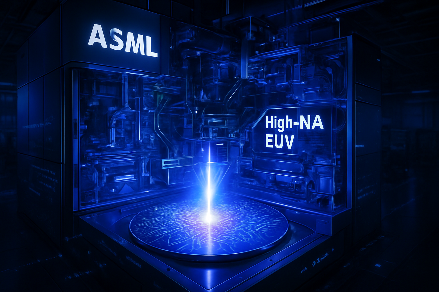
While 18A handles the current high-volume needs, the technological "north star" has shifted to the 14A (1.4nm) node. Currently in pilot production at Intel’s D1X "Mod 3" facility in Oregon, the 14A node is the world’s first to utilize High-Numerical Aperture (High-NA) Extreme Ultraviolet (EUV) lithography. These $380 million machines, manufactured by ASML (NASDAQ: ASML), allow for 1.7x smaller features compared to standard EUV tools. By being the first to master High-NA EUV, Intel has gained a projected two-year lead in lithographic resolution over rivals like TSMC (NYSE: TSM) and Samsung, who have opted for a more conservative transition to the new hardware.
The implementation of these ASML Twinscan EXE:5200B tools at the Ohio One "Silicon Heartland" site is currently the focus of Intel’s long-term infrastructure play. While the Ohio site has faced construction headwinds due to its sheer scale, the facility is being designed from the ground up to be the most advanced lithography hub on the planet. By the time Ohio becomes fully operational later this decade, it is expected to host a fleet of High-NA tools dedicated to the 14A-E (Extended) node, ensuring that the United States remains the center of gravity for sub-2nm fabrication.
The $5 Billion NVIDIA Alliance: A Strategic Guardrail
The reported $5 billion alliance between Intel and NVIDIA has sent shockwaves through the tech sector, fundamentally altering the competitive dynamics of the AI chip market. Under the terms of the deal, NVIDIA has secured a significant "private placement" of Intel stock, effectively becoming one of its largest strategic shareholders. While NVIDIA continues to rely on TSMC for its flagship Blackwell and Rubin-class GPUs, the $5 billion commitment serves as a "down payment" on future 18A and 14A capacity. This move provides NVIDIA with a vital domestic secondary source, mitigating the geopolitical risks associated with the Taiwan Strait.
For Intel Foundry, the NVIDIA alliance acts as the ultimate "seal of approval." Capturing a portion of the world's most valuable chip designer's business validates Intel's transition to a pure-play foundry model. Beyond manufacturing, the two companies are reportedly co-developing "super-stack" AI infrastructure. These systems integrate Intel’s x86 Xeon CPUs with NVIDIA GPUs through proprietary high-speed interconnects, optimized specifically for the 18A process. This deep integration is expected to yield AI training clusters that are 30% more power-efficient than previous generations, a critical factor as global data center energy consumption continues to skyrocket.
Market analysts suggest that this alliance places immense pressure on other fabless giants, such as Apple (NASDAQ: AAPL) and AMD (NASDAQ: AMD), to reconsider their manufacturing footprints. With NVIDIA effectively "camping out" at Intel's Arizona and Ohio sites, the available capacity for leading-edge nodes is becoming a scarce and highly contested resource. This has allowed Intel to demand more favorable terms and long-term volume commitments from new customers, stabilizing its once-volatile balance sheet.
Geopolitics and the Domestic Supply Chain
The success of the 18A rollout is being viewed in Washington D.C. as a triumph for the CHIPS and Science Act. As the largest recipient of federal grants and loans, Intel’s progress is inextricably linked to the U.S. government’s goal of producing 20% of the world's leading-edge chips by 2030. The "Arizona-to-Ohio" corridor represents a strategic redundancy in the global supply chain, ensuring that the critical components of the modern economy—from military AI to consumer smartphones—are no longer dependent on a single geographic point of failure.
However, the wider significance of this milestone extends beyond national security. The transition to 18A and 14A is happening just as the "Scaling Laws" of AI are being tested by the massive energy requirements of trillion-parameter models. By pioneering PowerVia and High-NA EUV, Intel is providing the hardware efficiency necessary for the next generation of generative AI. Without these advancements, the industry might have hit a "power wall" where the cost of electricity would have outpaced the cognitive gains of larger models.
Comparing this to previous milestones, the 18A launch is being likened to the transition from vacuum tubes to transistors or the introduction of the first microprocessor. It is not merely an incremental improvement; it is a foundational shift in how matter is manipulated at the atomic scale. The precision required to operate ASML’s High-NA tools is equivalent to "hitting a moving coin on the moon with a laser from Earth," a feat that Intel has now proven it can achieve in a high-volume industrial environment.
The Road to 10A: What Comes Next
As 18A matures and 14A moves toward HVM in 2027, Intel is already eyeing the "10A" (1nm) node. Future developments are expected to focus on Complementary FET (CFET) architectures, which stack n-type and p-type transistors on top of each other to save even more space. Experts predict that by 2028, the industry will see the first true 1nm chips, likely coming out of the Ohio One facility as it reaches its full operational stride.
The immediate challenge for Intel remains the "yield ramp." While 60% is a strong start for 18A, reaching the 80-90% yields typical of mature nodes will require months of iterative tuning. Furthermore, the integration of High-NA EUV into a seamless production flow at the Ohio site remains a logistical hurdle of unprecedented scale. The industry will be watching closely to see if Intel can maintain its aggressive cadence without the "execution stumbles" that plagued the company in the mid-2010s.
Summary and Final Thoughts
Intel’s manufacturing comeback, marked by the high-volume production of 18A in Arizona and the pioneering use of High-NA EUV for 14A, represents a turning point in the history of semiconductors. The $5 billion NVIDIA alliance further solidifies this resurgence, providing both the capital and the prestige necessary for Intel to reclaim its title as the world's premier chipmaker.
This development is a clear signal that the era of U.S. semiconductor manufacturing "outsourcing" is coming to an end. For the tech industry, the implications are profound: more competition in the foundry space, a more resilient global supply chain, and the hardware foundation required to sustain the AI revolution. In the coming months, all eyes will be on the performance of "Panther Lake" in the consumer market and the first 14A test wafers in Oregon, as Intel attempts to turn its technical lead into a permanent market advantage.
This content is intended for informational purposes only and represents analysis of current AI developments.
TokenRing AI delivers enterprise-grade solutions for multi-agent AI workflow orchestration, AI-powered development tools, and seamless remote collaboration platforms.
For more information, visit https://www.tokenring.ai/.