As of December 2025, the semiconductor industry stands at a pivotal juncture, navigating the evolving landscape where traditional silicon scaling, once the bedrock of technological advancement, faces increasing physical and economic hurdles. In response, a powerful dual strategy of relentless chip miniaturization and groundbreaking advanced packaging technologies has emerged as the new frontier, driving unprecedented improvements in performance, power efficiency, and device form factor. This synergistic approach is not merely extending the life of Moore's Law but fundamentally redefining how processing power is delivered, with profound implications for everything from artificial intelligence to consumer electronics.
The immediate significance of these advancements cannot be overstated. With the insatiable demand for computational horsepower driven by generative AI, high-performance computing (HPC), and the ever-expanding Internet of Things (IoT), the ability to pack more functionality into smaller, more efficient packages is critical. Advanced packaging, in particular, has transitioned from a supportive process to a core architectural enabler, allowing for the integration of diverse chiplets and components into sophisticated "mini-systems." This paradigm shift is crucial for overcoming bottlenecks like the "memory wall" and unlocking the next generation of intelligent, ubiquitous technology.
The Architecture of Tomorrow: Unpacking Advanced Semiconductor Technologies
The current wave of semiconductor innovation is characterized by a sophisticated interplay of nanoscale fabrication and ingenious integration techniques. While the pursuit of smaller transistors continues, with manufacturers pushing into 3-nanometer (nm) and 2nm processes—and Intel (NASDAQ: INTC) targeting 1.8nm mass production by 2026—the true revolution lies in how these tiny components are assembled. This contrasts sharply with previous eras where monolithic chip design and simple packaging sufficed.
At the forefront of this technical evolution are several key advanced packaging technologies:
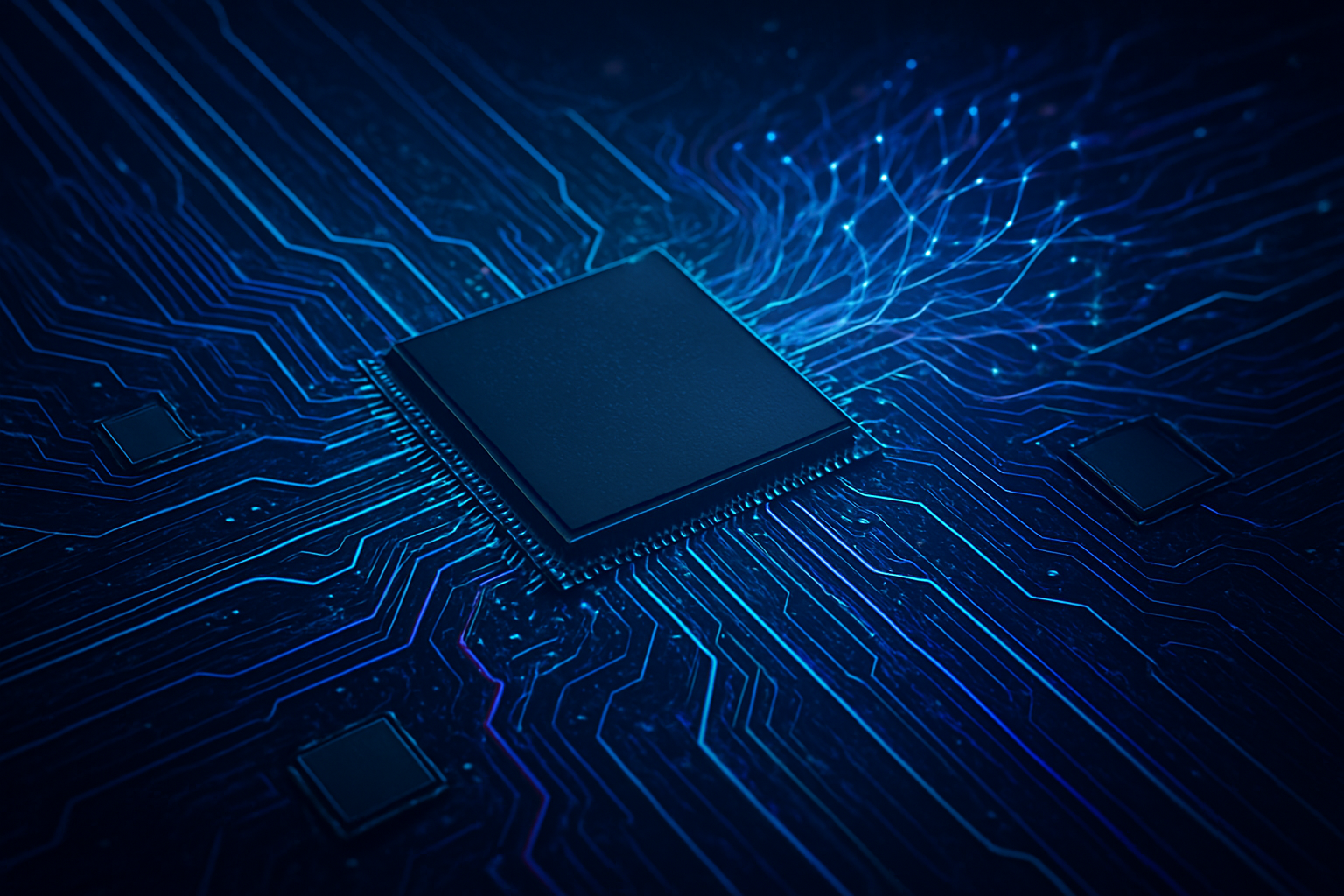
- 2.5D Integration: This technique involves placing multiple chiplets side-by-side on a silicon or organic interposer within a single package. It facilitates high-bandwidth communication between different dies, effectively bypassing the reticle limit (the maximum size of a single chip that can be manufactured monolithically). Leading examples include TSMC's (TPE: 2330) CoWoS, Samsung's (KRX: 005930) I-Cube, and Intel's (NASDAQ: INTC) EMIB. This differs from traditional packaging by enabling much tighter integration and higher data transfer rates between adjacent chips.
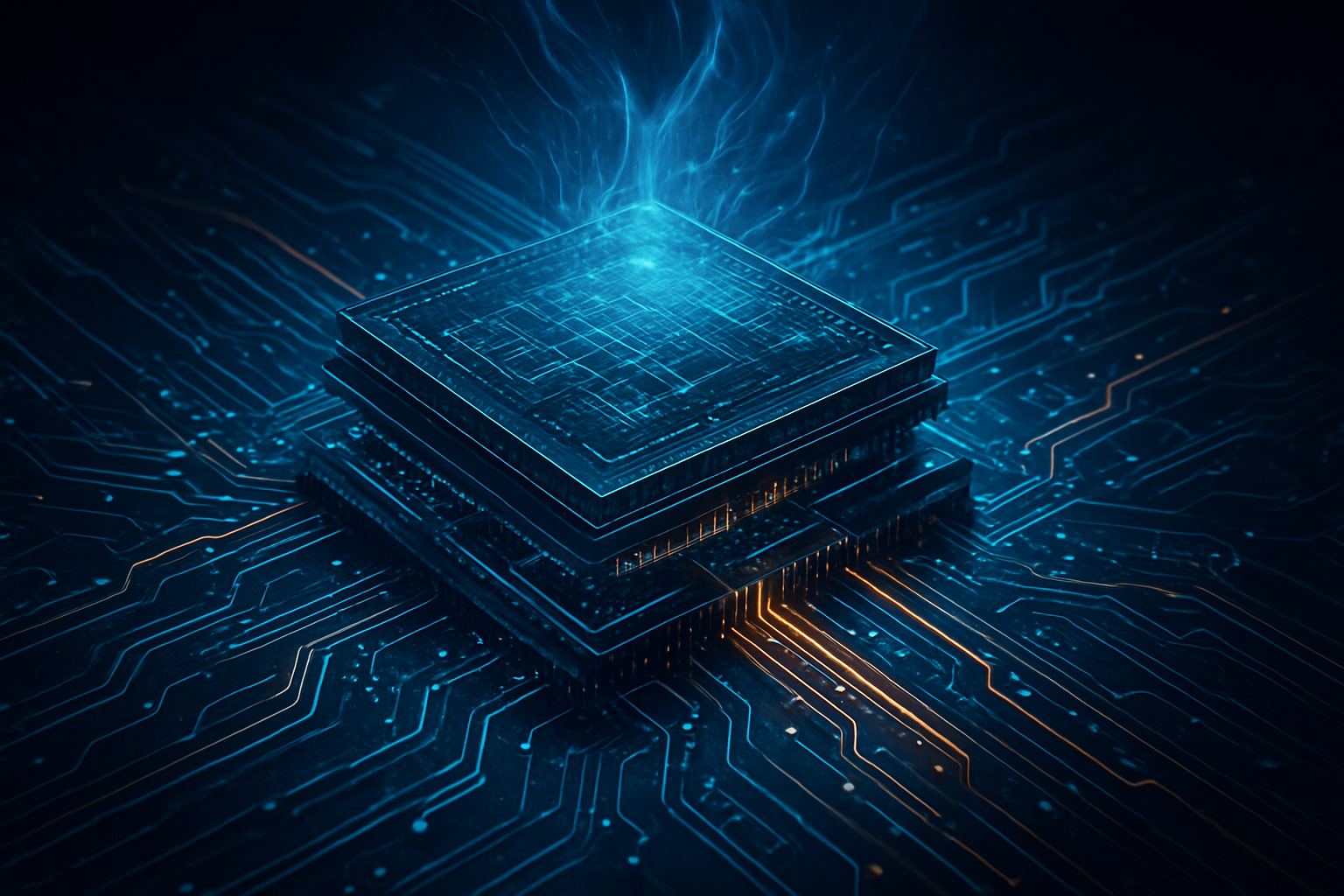
- 3D Stacking / 3D-IC: A more aggressive approach, 3D stacking involves vertically layering multiple dies—such as logic, memory, and sensors—and interconnecting them with Through-Silicon Vias (TSVs). TSVs are tiny vertical electrical connections that dramatically shorten data travel distances, significantly boosting bandwidth and reducing power consumption. High Bandwidth Memory (HBM), essential for AI accelerators, is a prime example, placing vast amounts of memory directly atop or adjacent to the processing unit. This vertical integration offers a far smaller footprint and superior performance compared to traditional side-by-side placement of discrete components.
- Chiplets: These are small, modular integrated circuits that can be combined and interconnected to form a complete system. This modularity offers unprecedented design flexibility, allowing designers to mix and match specialized chiplets (e.g., CPU, GPU, I/O, memory controllers) from different process nodes or even different manufacturers. This approach significantly reduces development time and cost, improves manufacturing yields by isolating defects to smaller components, and enables custom solutions for specific applications. It represents a departure from the "system-on-a-chip" (SoC) philosophy by distributing functionality across multiple, specialized dies.
- System-in-Package (SiP) and Wafer-Level Packaging (WLP): SiP integrates multiple ICs and passive components into a single package for compact, efficient designs, particularly in mobile and IoT devices. WLP and Fan-Out Wafer-Level Packaging (FO-WLP/FO-PLP) package chips directly at the wafer level, leading to smaller, more power-efficient packages with increased input/output density.
Initial reactions from the AI research community and industry experts are overwhelmingly positive. The consensus is that advanced packaging is no longer merely an optimization but a fundamental requirement for pushing the boundaries of AI, especially with the emergence of large language models and generative AI. The ability to overcome memory bottlenecks and deliver unprecedented bandwidth is seen as critical for training and deploying increasingly complex AI models. Experts highlight the necessity of co-designing chips and their packaging from the outset, rather than treating packaging as an afterthought, to fully realize the potential of these technologies.
Reshaping the Competitive Landscape: Who Benefits and Who Adapts?
The advancements in miniaturization and advanced packaging are profoundly reshaping the competitive dynamics within the semiconductor and broader technology industries. Companies with significant R&D investments and established capabilities in these areas stand to gain substantial strategic advantages, while others will need to rapidly adapt or risk falling behind.
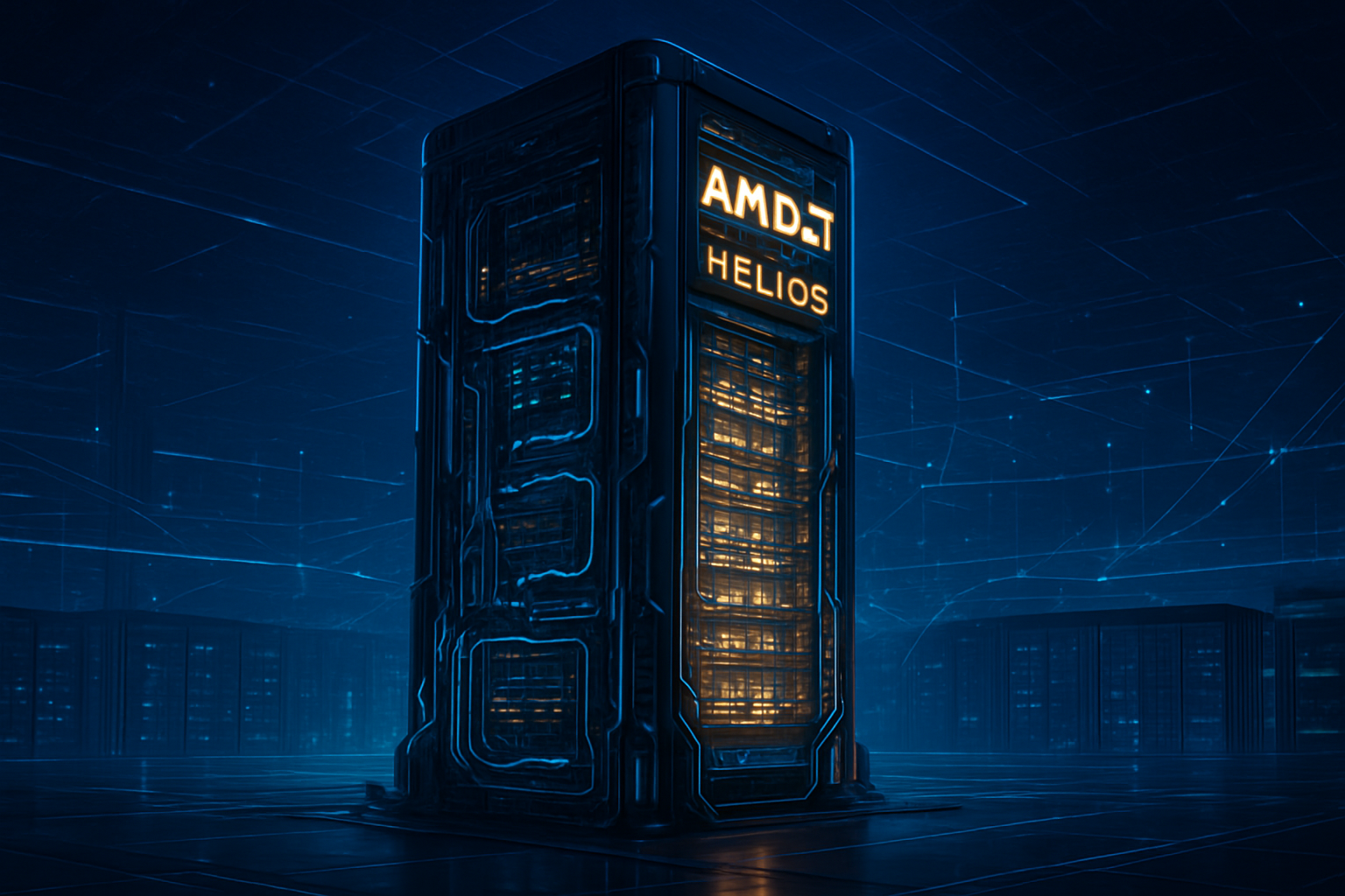
Leading semiconductor manufacturers like Taiwan Semiconductor Manufacturing Company (TSMC) (TPE: 2330), Intel Corporation (NASDAQ: INTC), and Samsung Electronics Co., Ltd. (KRX: 005930) are at the forefront, heavily investing in and expanding their advanced packaging capacities. TSMC, with its CoWoS (Chip-on-Wafer-on-Substrate) and InFO (Integrated Fan-Out) technologies, has become a critical enabler for AI chip developers, including NVIDIA Corporation (NASDAQ: NVDA) and Advanced Micro Devices, Inc. (NASDAQ: AMD). These foundries are not just manufacturing chips but are now integral partners in designing the entire system-in-package, offering competitive differentiation through their packaging expertise.
NVIDIA (NASDAQ: NVDA) and AMD (NASDAQ: AMD) are prime beneficiaries, leveraging 2.5D and 3D stacking with HBM to power their cutting-edge GPUs and AI accelerators. Their ability to deliver unparalleled memory bandwidth and computational density directly stems from these packaging innovations, giving them a significant edge in the booming AI and high-performance computing markets. Similarly, memory giants like Micron Technology, Inc. (NASDAQ: MU) and SK Hynix Inc. (KRX: 000660), which produce HBM, are seeing surging demand and investing heavily in next-generation 3D memory stacks.
The competitive implications are significant for major AI labs and tech giants. Companies developing their own custom AI silicon, such as Alphabet Inc. (NASDAQ: GOOG, GOOGL) with its TPUs and Amazon.com, Inc. (NASDAQ: AMZN) with its Graviton and Trainium chips, are increasingly relying on advanced packaging to optimize their designs for specific workloads. This allows them to achieve superior performance-per-watt and cost efficiency compared to off-the-shelf solutions.
Potential disruption to existing products or services includes a shift away from purely monolithic chip designs towards more modular, chiplet-based architectures. This could democratize chip design to some extent, allowing smaller startups to innovate by integrating specialized chiplets without the prohibitively high costs of designing an entire SoC from scratch. However, it also creates a new set of challenges related to chiplet interoperability and standardization. Companies that fail to embrace heterogeneous integration and advanced packaging risk being outmaneuvered by competitors who can deliver more powerful, compact, and energy-efficient solutions across various market segments, from data centers to edge devices.
A New Era of Computing: Wider Significance and Broader Trends
The relentless pursuit of miniaturization and the rise of advanced packaging technologies are not isolated developments; they represent a fundamental shift in the broader AI and computing landscape, ushering in what many are calling the "More than Moore" era. This paradigm acknowledges that performance gains are now derived not just from shrinking transistors but equally from innovative architectural and packaging solutions.
This trend fits perfectly into the broader AI landscape, where the sheer scale of data and complexity of models demand unprecedented computational resources. Advanced packaging directly addresses critical bottlenecks, particularly the "memory wall," which has long limited the performance of AI accelerators. By placing memory closer to the processing units, these technologies enable faster data access, higher bandwidth, and lower latency, which are absolutely essential for training and inference of large language models (LLMs), generative AI, and complex neural networks. The market for generative AI chips alone is projected to exceed $150 billion in 2025, underscoring the critical role of these packaging innovations.
The impacts extend far beyond AI. In consumer electronics, these advancements are enabling smaller, more powerful, and energy-efficient mobile devices, wearables, and IoT sensors. The automotive industry, with its rapidly evolving autonomous driving and electric vehicle technologies, also heavily relies on high-performance, compact semiconductor solutions for advanced driver-assistance systems (ADAS) and AI-powered control units.
While the benefits are immense, potential concerns include the increasing complexity and cost of manufacturing. Advanced packaging processes require highly specialized equipment, materials, and expertise, leading to higher development and production costs. Thermal management for densely packed 3D stacks also presents significant engineering challenges, as heat dissipation becomes more difficult in confined spaces. Furthermore, the burgeoning chiplet ecosystem necessitates robust standardization efforts to ensure interoperability and foster a truly open and competitive market.
Compared to previous AI milestones, such as the initial breakthroughs in deep learning or the development of specialized AI accelerators, the current focus on packaging represents a foundational shift. It's not just about algorithmic innovation or new chip architectures; it's about the very physical realization of those innovations, enabling them to reach their full potential. This emphasis on integration and efficiency is as critical as any algorithmic breakthrough in driving the next wave of AI capabilities.
The Road Ahead: Future Developments and Expert Predictions
The trajectory of miniaturization and advanced packaging points towards an exciting future, with continuous innovation expected in both the near and long term. Experts predict a future where chip design and packaging are inextricably linked, co-architected from the ground up to optimize performance, power, and cost.
In the near term, we can expect further refinement and widespread adoption of existing advanced packaging technologies. This includes the maturation of 2nm and even 1.8nm process nodes, coupled with more sophisticated 2.5D and 3D integration techniques. Innovations in materials science will play a crucial role, with developments in glass interposers offering superior electrical and thermal properties compared to silicon, and new high-performance thermal interface materials addressing heat dissipation challenges in dense stacks. The standardization of chiplet interfaces, such as UCIe (Universal Chiplet Interconnect Express), is also expected to gain significant traction, fostering a more open and modular ecosystem for chip design.
Longer-term developments include the exploration of truly revolutionary approaches like Holographic Metasurface Nano-Lithography (HMNL), a new 3D printing method that could enable entirely new 3D package architectures and previously impossible designs, such as fully 3D-printed electronic packages or components integrated into unconventional spaces. The concept of "system-on-package" (SoP) will evolve further, integrating not just digital and analog components but also optical and even biological elements into highly compact, functional units.
Potential applications and use cases on the horizon are vast. Beyond more powerful AI and HPC, these technologies will enable hyper-miniaturized sensors for ubiquitous IoT, advanced medical implants, and next-generation augmented and virtual reality devices with unprecedented display resolutions and processing power. Autonomous systems, from vehicles to drones, will benefit from highly integrated, robust, and power-efficient processing units.
Challenges that need to be addressed include the escalating cost of advanced manufacturing facilities, the complexity of design and verification for heterogeneous integrated systems, and the ongoing need for improved thermal management solutions. Experts predict a continued consolidation in the advanced packaging market, with major players investing heavily to capture market share. They also foresee a greater emphasis on sustainability in manufacturing processes, given the environmental impact of chip production. The drive for "disaggregated computing" – breaking down large processors into smaller, specialized chiplets – will continue, pushing the boundaries of what's possible in terms of customization and efficiency.
A Defining Moment for the Semiconductor Industry
In summary, the confluence of continuous chip miniaturization and advanced packaging technologies represents a defining moment in the history of the semiconductor industry. As traditional scaling approaches encounter fundamental limits, these innovative strategies have become the primary engines for driving performance improvements, power efficiency, and form factor reduction across the entire spectrum of electronic devices. The transition from monolithic chips to modular, heterogeneously integrated systems marks a profound shift, enabling the exponential growth of artificial intelligence, high-performance computing, and a myriad of other transformative technologies.
This development's significance in AI history is paramount. It addresses the physical bottlenecks that could otherwise stifle the progress of increasingly complex AI models, particularly in the realm of generative AI and large language models. By enabling higher bandwidth, lower latency, and greater computational density, advanced packaging is directly facilitating the next generation of AI capabilities, from faster training to more efficient inference at the edge.
Looking ahead, the long-term impact will be a world where computing is even more pervasive, powerful, and seamlessly integrated into our lives. Devices will become smarter, smaller, and more energy-efficient, unlocking new possibilities in health, communication, and automation. What to watch for in the coming weeks and months includes further announcements from leading foundries regarding their next-generation packaging roadmaps, new product launches from AI chip developers leveraging these advanced techniques, and continued efforts towards standardization within the chiplet ecosystem. The race to integrate more, faster, and smaller components is on, and the outcomes will shape the technological landscape for decades to come.
This content is intended for informational purposes only and represents analysis of current AI developments.
TokenRing AI delivers enterprise-grade solutions for multi-agent AI workflow orchestration, AI-powered development tools, and seamless remote collaboration platforms.
For more information, visit https://www.tokenring.ai/.