The relentless pursuit of smaller, more powerful, and energy-efficient chips is not just an incremental improvement; it's a fundamental imperative reshaping the entire technology landscape. As of December 2025, the semiconductor industry is at a pivotal juncture, where the continuous miniaturization of transistors, coupled with revolutionary advancements in advanced packaging, is driving an unprecedented surge in computational capabilities. This dual strategy is the backbone of modern artificial intelligence (AI), enabling breakthroughs in generative AI, high-performance computing (HPC), and pushing intelligence to the very edge of our devices. The ability to pack billions of transistors into microscopic spaces, and then ingeniously interconnect them, is fueling a new era of innovation, making smarter, faster, and more integrated technologies a reality.
Technical Milestones in Miniaturization
The current wave of chip miniaturization goes far beyond simply shrinking transistors; it involves fundamental architectural shifts and sophisticated integration techniques. Leading foundries are aggressively pushing into sub-3 nanometer (nm) process nodes. Taiwan Semiconductor Manufacturing Company (TSMC) (NYSE: TSM) is on track for volume production of its 2nm (N2) process in the second half of 2025, transitioning from FinFET to Gate-All-Around (GAA) nanosheet transistors. This shift offers superior control over electrical current, significantly reducing leakage and improving power efficiency. TSMC is also developing an A16 (1.6nm) process for late 2026, which will integrate nanosheet transistors with a novel Super Power Rail (SPR) solution for further performance and density gains.
Similarly, Intel Corporation (NASDAQ: INTC) is advancing with its 18A (1.8nm) process, which is considered "ready" for customer projects with high-volume manufacturing expected by Q4 2025. Intel's 18A node leverages RibbonFET GAA technology and introduces PowerVia backside power delivery. PowerVia is a groundbreaking innovation that moves the power delivery network to the backside of the wafer, separating power and signal routing. This significantly improves density, reduces resistive power delivery droop, and enhances performance by freeing up routing space on the front side. Samsung Electronics (KRX: 005930) was the first to commercialize GAA transistors with its 3nm process and plans to launch its third generation of GAA technology (MBCFET) with its 2nm process in 2025, targeting mobile chips.
Beyond traditional 2D scaling, 3D stacking and advanced packaging are becoming increasingly vital. Technologies like Through-Silicon Vias (TSVs) enable multiple layers of integrated circuits to be stacked and interconnected directly, drastically shortening interconnect lengths for faster signal transmission and lower power consumption. Hybrid bonding, connecting metal pads directly without copper bumps, allows for significantly higher interconnect density. Monolithic 3D integration, where layers are built sequentially, promises even denser vertical connections and has shown potential for 100- to 1,000-fold improvements in energy-delay product for AI workloads. These approaches represent a fundamental shift from monolithic System-on-Chip (SoC) designs, overcoming limitations in reticle size, manufacturing yields, and the "memory wall" by allowing for vertical integration and heterogeneous chiplet integration. Initial reactions from the AI research community and industry experts are overwhelmingly positive, viewing these advancements as critical enablers for the next generation of AI and high-performance computing, particularly for generative AI and large language models.
Industry Shifts and Competitive Edge
The profound implications of chip miniaturization and advanced packaging are reverberating across the entire tech industry, fundamentally altering competitive landscapes and market dynamics. AI companies stand to benefit immensely, as these technologies are crucial for faster processing, improved energy efficiency, and greater component integration essential for high-performance AI. Companies like NVIDIA Corporation (NASDAQ: NVDA) and Advanced Micro Devices (NASDAQ: AMD) are prime beneficiaries, leveraging 2.5D and 3D stacking with High Bandwidth Memory (HBM) to power their cutting-edge GPUs and AI accelerators, giving them a significant edge in the booming AI and HPC markets.
Tech giants are strategically investing heavily in these advancements. Foundries like TSMC, Intel, and Samsung are not just manufacturers but integral partners, expanding their advanced packaging capacities (e.g., TSMC's CoWoS, Intel's EMIB, Samsung's I-Cube). Cloud providers such as Alphabet (NASDAQ: GOOGL) with its TPUs and Amazon.com, Inc. (NASDAQ: AMZN) with Graviton and Trainium chips, along with Microsoft Corporation (NASDAQ: MSFT) and its Azure Maia 100, are developing custom AI silicon optimized for their specific workloads, gaining superior performance-per-watt and cost efficiency. This trend highlights a move towards vertical integration, where hardware, software, and packaging are co-designed for maximum impact.
For startups, advanced packaging and chiplet architectures present a dual scenario. On one hand, modular, chiplet-based designs can democratize chip design, allowing smaller players to innovate by integrating specialized chiplets without the prohibitive costs of designing an entire SoC from scratch. Companies like Silicon Box and DEEPX are securing significant funding in this space. On the other hand, startups face challenges related to chiplet interoperability and the rapid obsolescence of leading-edge chips. The primary disruption is a significant shift away from purely monolithic chip designs towards more modular, chiplet-based architectures. Companies that fail to embrace heterogeneous integration and advanced packaging risk being outmaneuvered, as the market for generative AI chips alone is projected to exceed $150 billion in 2025.
AI's Broader Horizon
The wider significance of chip miniaturization and advanced packaging extends far beyond mere technical specifications; it represents a foundational shift in the broader AI landscape and trends. These innovations are not just enabling AI's current capabilities but are critical for its future trajectory. The insatiable demand from generative AI and large language models (LLMs) is a primary catalyst, with advanced packaging, particularly in overcoming memory bottlenecks and delivering high bandwidth, being crucial for both training and inference of these complex models. This also facilitates the transition of AI from cloud-centric operations to edge devices, enabling powerful yet energy-efficient AI in smartphones, wearables, IoT sensors, and even miniature PCs capable of running LLMs locally.
The impacts are profound, leading to enhanced performance, improved energy efficiency (drastically reducing energy required for data movement), and smaller form factors that push AI into new application domains. Radical miniaturization is enabling novel applications such as ultra-thin, wireless brain implants (like BISC) for brain-computer interfaces, advanced driver-assistance systems (ADAS) in autonomous vehicles, and even programmable microscopic robots for potential medical applications. This era marks a "symbiotic relationship between software and silicon," where hardware advancements are as critical as algorithmic breakthroughs. The economic impact is substantial, with the advanced packaging market for data center AI chips projected for explosive growth, from $5.6 billion in 2024 to $53.1 billion by 2030, a CAGR of over 40%.
However, concerns persist. The manufacturing complexity and staggering costs of developing and producing advanced packaging and sub-2nm process nodes are immense. Thermal management in densely integrated packages remains a significant challenge, requiring innovative cooling solutions. Supply chain resilience is also a critical issue, with geopolitical concentration of advanced manufacturing creating vulnerabilities. Compared to previous AI milestones, which were often driven by algorithmic advancements (e.g., expert systems, machine learning, deep learning), the current phase is defined by hardware innovation that is extending and redefining Moore's Law, fundamentally overcoming the "memory wall" that has long hampered AI performance. This hardware-software synergy is foundational for the next generation of AI capabilities.
The Road Ahead: Future Innovations
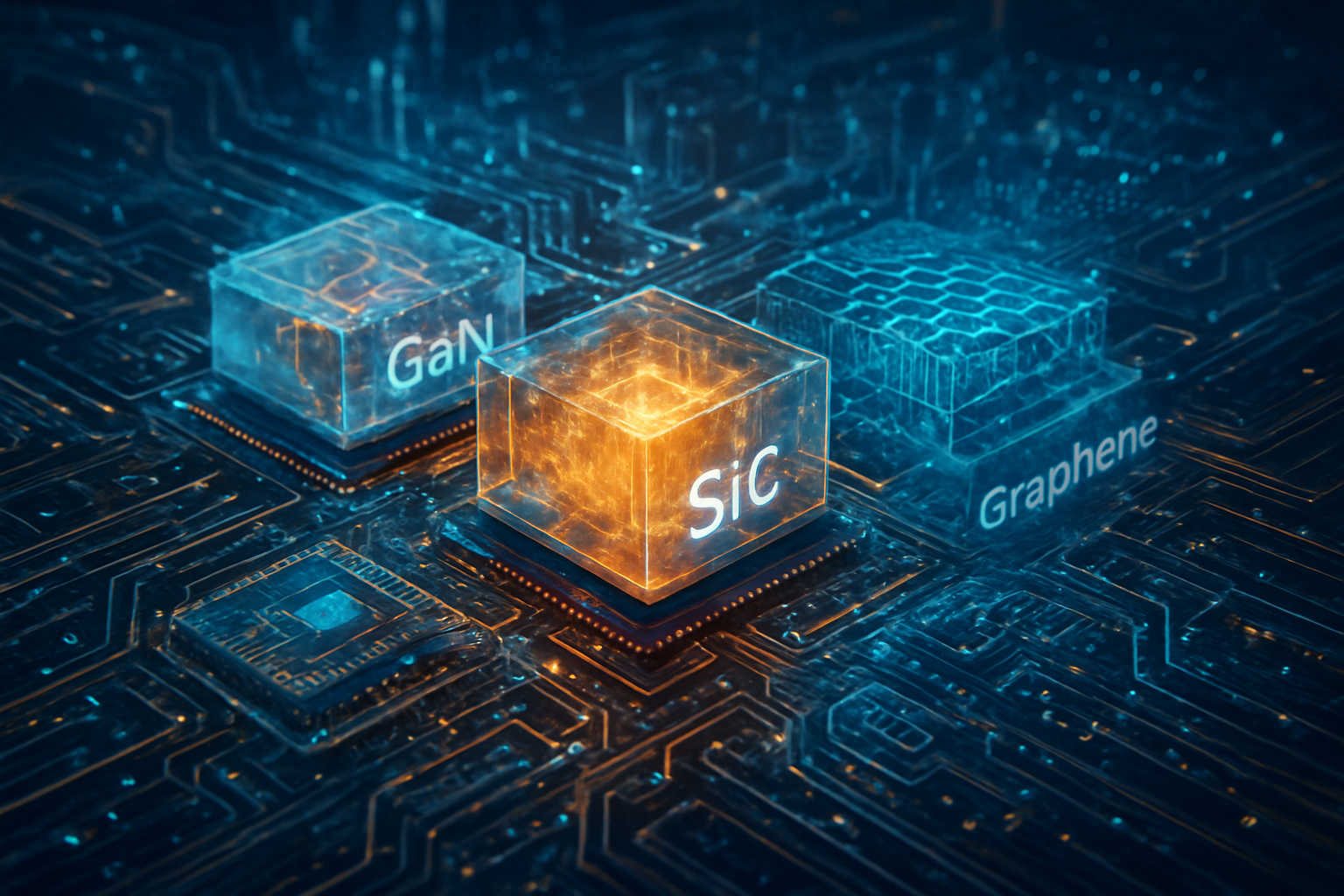
Looking ahead, the future of chip miniaturization and advanced packaging promises even more radical transformations. In the near term, the industry will see the widespread adoption and refinement of 2nm and 1.8nm process nodes, alongside increasingly sophisticated 2.5D and 3D integration techniques. The push beyond 1nm will likely involve exploring novel transistor architectures and materials beyond silicon, such as carbon nanotube transistors (CNTs) and 2D materials like graphene, offering superior conductivity and minimal leakage. Advanced lithography, particularly High-NA EUV, will be crucial for pushing feature sizes below 10nm and enabling future 1.4nm nodes around 2027.
Longer-term developments include the maturation of hybrid bonding for ultra-fine pitch vertical interconnects, crucial for next-generation High-Bandwidth Memory (HBM) beyond 16-Hi or 20-Hi layers. Co-Packaged Optics (CPO) will integrate optical interconnects directly into advanced packages, overcoming electrical bandwidth limitations for exascale AI systems. New interposer materials like glass are gaining traction due to superior electrical and thermal properties. Experts also predict the increasing integration of quantum computing components into the semiconductor ecosystem, leveraging established fabrication techniques for silicon-based qubits. Potential applications span more powerful and energy-efficient AI accelerators, robust solutions for 5G and 6G networks, hyper-miniaturized IoT sensors, advanced automotive systems, and groundbreaking medical technologies.
Despite the exciting prospects, significant challenges remain. Physical limits at the sub-nanometer scale introduce quantum effects and extreme heat dissipation issues, demanding innovative thermal management solutions like microfluidic cooling or diamond materials. The escalating costs of advanced manufacturing, with new fabs costing tens of billions of dollars and High-NA EUV machines nearing $400 million, pose substantial economic hurdles. Manufacturing complexity, yield management for multi-die assemblies, and the immaturity of new material ecosystems are also critical challenges. Experts predict continued market growth driven by AI, a sustained "More than Moore" era where packaging is central, and a co-architected approach to chip design and packaging.
A New Era of Intelligence
In summary, the ongoing revolution in chip miniaturization and advanced packaging represents the most significant hardware transformation underpinning the current and future trajectory of Artificial Intelligence. Key takeaways include the transition to a "More-than-Moore" era, where advanced packaging is a core architectural enabler, not just a back-end process. This shift is fundamentally driven by the insatiable demands of generative AI and high-performance computing, which require unprecedented levels of computational power, memory bandwidth, and energy efficiency. These advancements are directly overcoming historical bottlenecks like the "memory wall," allowing AI models to grow in complexity and capability at an exponential rate.
This development's significance in AI history cannot be overstated; it is the physical foundation upon which the next generation of intelligent systems will be built. It is enabling a future of ubiquitous and intelligent devices, where AI is seamlessly integrated into every facet of our lives, from autonomous vehicles to advanced medical implants. The long-term impact will be a world defined by co-architected designs, heterogeneous integration as the norm, and a relentless pursuit of sustainability in computing. The industry is witnessing a profound and enduring change, ensuring that the spirit of Moore's Law continues to drive progress, albeit through new and innovative means.
In the coming weeks and months, watch for continued market growth in advanced packaging, particularly for AI-driven applications, with revenues projected to significantly outpace the rest of the chip industry. Keep an eye on the roadmaps of major AI chip developers like NVIDIA and AMD, as their next-generation architectures will define the capabilities of future AI systems. The maturation of novel packaging technologies such as panel-level packaging and hybrid bonding, alongside the further development of neuromorphic and photonic chips, will be critical indicators of progress. Finally, geopolitical factors and supply chain dynamics will continue to influence the availability and cost of these cutting-edge components, underscoring the strategic importance of semiconductor manufacturing in the global economy.
This content is intended for informational purposes only and represents analysis of current AI developments.
TokenRing AI delivers enterprise-grade solutions for multi-agent AI workflow orchestration, AI-powered development tools, and seamless remote collaboration platforms.
For more information, visit https://www.tokenring.ai/.