HSINCHU, Taiwan – October 17, 2025 – Taiwan Semiconductor Manufacturing Company (TSMC) (NYSE: TSM), the world's leading dedicated semiconductor foundry, announced robust financial results for the third quarter of 2025 on October 16, 2025. The earnings report, released just a day before the current date, revealed significant growth driven primarily by unprecedented demand for advanced artificial intelligence (AI) chips and High-Performance Computing (HPC). These strong results underscore TSMC's critical position as the "backbone" of the semiconductor industry and carry immediate positive implications for the broader tech market, validating the ongoing "AI supercycle" that is reshaping global technology.
TSMC's exceptional performance, with revenue and net income soaring past analyst expectations, highlights its indispensable role in enabling the next generation of AI innovation. The company's continuous leadership in advanced process nodes ensures that virtually every major technological advancement in AI, from sophisticated large language models to cutting-edge autonomous systems, is built upon its foundational silicon. This quarterly triumph not only reflects TSMC's operational excellence but also provides a crucial barometer for the health and trajectory of the entire AI hardware ecosystem.
Engineering the Future: TSMC's Technical Prowess and Financial Strength
TSMC's Q3 2025 financial highlights paint a picture of extraordinary growth and profitability. The company reported consolidated revenue of NT$989.92 billion (approximately US$33.10 billion), marking a substantial year-over-year increase of 30.3% (or 40.8% in U.S. dollar terms) and a sequential increase of 6.0% from Q2 2025. Net income for the quarter reached a record high of NT$452.30 billion (approximately US$14.78 billion), representing a 39.1% increase year-over-year and 13.6% from the previous quarter. Diluted earnings per share (EPS) stood at NT$17.44 (US$2.92 per ADR unit).
The company maintained strong profitability, with a gross margin of 59.5%, an operating margin of 50.6%, and a net profit margin of 45.7%. Advanced technologies, specifically 3-nanometer (nm), 5nm, and 7nm processes, were pivotal to this performance, collectively accounting for 74% of total wafer revenue. Shipments of 3nm process technology contributed 23% of total wafer revenue, while 5nm accounted for 37%, and 7nm for 14%. This heavy reliance on advanced nodes for revenue generation differentiates TSMC from previous semiconductor manufacturing approaches, which often saw slower transitions to new technologies and more diversified revenue across older nodes. TSMC's pure-play foundry model, pioneered in 1987, has allowed it to focus solely on manufacturing excellence and cutting-edge research, attracting all major fabless chip designers.
Revenue was significantly driven by the High-Performance Computing (HPC) and smartphone platforms, which constituted 57% and 30% of net revenue, respectively. North America remained TSMC's largest market, contributing 76% of total net revenue. The overwhelming demand for AI-related applications and HPC chips, which drove TSMC's record-breaking performance, provides strong validation for the ongoing "AI supercycle." Initial reactions from the industry and analysts have been overwhelmingly positive, with TSMC's results surpassing expectations and reinforcing confidence in the long-term growth trajectory of the AI market. TSMC Chairman C.C. Wei noted that AI demand is "stronger than we previously expected," signaling a robust outlook for the entire AI hardware ecosystem.
Ripple Effects: How TSMC's Dominance Shapes the AI and Tech Landscape
TSMC's strong Q3 2025 results and its dominant position in advanced chip manufacturing have profound implications for AI companies, major tech giants, and burgeoning startups alike. Its unrivaled market share, estimated at over 70% in the global pure-play wafer foundry market and an even more pronounced 92% in advanced AI chip manufacturing, makes it the "unseen architect" of the AI revolution.
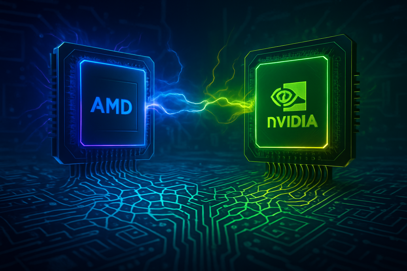
Nvidia (NASDAQ: NVDA), a leading designer of AI GPUs, stands as a primary beneficiary and is directly dependent on TSMC for the production of its high-powered AI chips. TSMC's robust performance and raised guidance are a positive indicator for Nvidia's continued growth in the AI sector, boosting market sentiment. Similarly, AMD (NASDAQ: AMD) relies on TSMC for manufacturing its CPUs, GPUs, and AI accelerators, aligning with AMD CEO's projection of significant annual growth in the high-performance chip market. Apple (NASDAQ: AAPL) remains a key customer, with TSMC producing its A19, A19 Pro, and M5 processors on advanced nodes like N3P, ensuring Apple's ability to innovate with its proprietary silicon. Other tech giants like Google (NASDAQ: GOOGL), Amazon (NASDAQ: AMZN), Microsoft (NASDAQ: MSFT), Broadcom (NASDAQ: AVGO), and Meta Platforms (NASDAQ: META) also heavily rely on TSMC, either directly for custom AI chips (ASICs) or indirectly through their purchases of Nvidia and AMD components, as the "explosive growth in token volume" from large language models drives the need for more leading-edge silicon.
TSMC's continued lead further entrenches its near-monopoly, making it challenging for competitors like Samsung Foundry and Intel Foundry Services (NASDAQ: INTC) to catch up in terms of yield and scale at the leading edge (e.g., 3nm and 2nm). This reinforces TSMC's pricing power and strategic importance. For AI startups, while TSMC's dominance provides access to unparalleled technology, it also creates significant barriers to entry due to the immense capital and technological requirements. Startups with innovative AI chip designs must secure allocation with TSMC, often competing with tech giants for limited advanced node capacity.
The strategic advantage gained by companies securing access to TSMC's advanced manufacturing capacity is critical for producing the most powerful, energy-efficient chips necessary for competitive AI models and devices. TSMC's raised capital expenditure guidance for 2025 ($40-42 billion, with 70% dedicated to advanced front-end process technologies) signals its commitment to meeting this escalating demand and maintaining its technological lead. This positions key customers to continue pushing the boundaries of AI and computing performance, ensuring the "AI megatrend" is not just a cyclical boom but a structural shift that TSMC is uniquely positioned to enable.
Global Implications: AI's Engine and Geopolitical Currents
TSMC's strong Q3 2025 results are more than just a financial success story; they are a profound indicator of the accelerating AI revolution and its wider significance for global technology and geopolitics. The company's performance highlights the intricate interdependencies within the tech ecosystem, impacting global supply chains and navigating complex international relations.
TSMC's success is intrinsically linked to the "AI boom" and the emerging "AI Supercycle," characterized by an insatiable global demand for advanced computing power. The global AI chip market alone is projected to exceed $150 billion in 2025. This widespread integration of AI across industries necessitates specialized and increasingly powerful silicon, solidifying TSMC's indispensable role in powering these technological advancements. The rapid progression to sub-2nm nodes, along with the critical role of advanced packaging solutions like CoWoS (Chip-on-Wafer-on-Substrate) and SoIC (System-on-Integrated-Chips), are key technological trends that TSMC is spearheading to meet the escalating demands of AI, fundamentally transforming the semiconductor industry itself.
TSMC's central position creates both significant strength and inherent vulnerabilities within global supply chains. The industry is currently undergoing a massive transformation, shifting from a hyper-efficient, geographically concentrated model to one prioritizing redundancy and strategic independence. This pivot is driven by lessons from past disruptions like the COVID-19 pandemic and escalating geopolitical tensions. Governments worldwide, through initiatives such as the U.S. CHIPS Act and the European Chips Act, are investing trillions to diversify manufacturing capabilities. However, the concentration of advanced semiconductor manufacturing in East Asia, particularly Taiwan, which produces 100% of semiconductors with nodes under 10 nanometers, creates significant strategic risks. Any disruption to Taiwan's semiconductor production could have "catastrophic consequences" for global technology.
Taiwan's dominance in the semiconductor industry, spearheaded by TSMC, has transformed the island into a strategic focal point in the intensifying US-China technological competition. TSMC's control over 90% of cutting-edge chip production, while an economic advantage, is increasingly viewed as a "strategic liability" for Taiwan. The U.S. has implemented stringent export controls on advanced AI chips and manufacturing equipment to China, leading to a "fractured supply chain." TSMC is strategically responding by expanding its production footprint beyond Taiwan, including significant investments in the U.S. (Arizona), Japan, and Germany. This global expansion, while costly, is crucial for mitigating geopolitical risks and ensuring long-term supply chain resilience. The current AI expansion is often compared to the Dot-Com Bubble, but many analysts argue it is fundamentally different and more robust, driven by profitable global companies reinvesting substantial free cash flow into real infrastructure, marking a structural transformation where semiconductor innovation underpins a lasting technological shift.
The Road Ahead: Next-Generation Silicon and Persistent Challenges
TSMC's commitment to pushing the boundaries of semiconductor technology is evident in its aggressive roadmap for process nodes and advanced packaging, profoundly influencing the trajectory of AI development. The company's future developments are poised to enable even more powerful and efficient AI models.
Near-Term Developments (2nm): TSMC's 2-nanometer (2nm) process, known as N2, is slated for mass production in the second half of 2025. This node marks a significant transition to Gate-All-Around (GAA) nanosheet transistors, offering a 15% performance improvement or a 25-30% reduction in power consumption compared to 3nm, alongside a 1.15x increase in transistor density. Major customers, including NVIDIA, AMD, Google, Amazon, and OpenAI, are designing their next-generation AI accelerators and custom AI chips on this advanced node, with Apple also anticipated to be an early adopter. TSMC is also accelerating 2nm chip production in the United States, with facilities in Arizona expected to commence production by the second half of 2026.
Long-Term Developments (1.6nm, 1.4nm, and Beyond): Following the 2nm node, TSMC has outlined plans for even more advanced technologies. The 1.6nm (A16) node, scheduled for 2026, is projected to offer a further 15-20% reduction in energy usage, particularly beneficial for power-intensive HPC applications. The 1.4nm (A14) node, expected in the second half of 2028, promises a 15% performance increase or a 30% reduction in energy consumption compared to 2nm processors, along with higher transistor density. TSMC is also aggressively expanding its advanced packaging capabilities like CoWoS, aiming to quadruple output by the end of 2025 and reach 130,000 wafers per month by 2026, and plans for mass production of SoIC (3D stacking) in 2025. These advancements will facilitate enhanced AI models, specialized AI accelerators, and new AI use cases across various sectors.
However, TSMC and the broader semiconductor industry face several significant challenges. Power consumption by AI chips creates substantial environmental and economic concerns, which TSMC is addressing through collaborations on AI software and designing A16 nanosheet process to reduce power consumption. Geopolitical risks, particularly Taiwan-China tensions and the US-China tech rivalry, continue to impact TSMC's business and drive costly global diversification efforts. The talent shortage in the semiconductor industry is another critical hurdle, impacting production and R&D, leading TSMC to increase worker compensation and invest in training. Finally, the increasing costs of research, development, and manufacturing at advanced nodes pose a significant financial hurdle, potentially impacting the cost of AI infrastructure and consumer electronics. Experts predict sustained AI-driven growth for TSMC, with its technological leadership continuing to dictate the pace of technological progress in AI, alongside intensified competition and strategic global expansion.
A New Epoch: Assessing TSMC's Enduring Legacy in AI
TSMC's stellar Q3 2025 results are far more than a quarterly financial report; they represent a pivotal moment in the ongoing AI revolution, solidifying the company's status as the undisputed titan and fundamental enabler of this transformative era. Its record-breaking revenue and profit, driven overwhelmingly by demand for advanced AI and HPC chips, underscore an indispensable role in the global technology landscape. With nearly 90% of the world's most advanced logic chips and well over 90% of AI-specific chips flowing from its foundries, TSMC's silicon is the foundational bedrock upon which virtually every major AI breakthrough is built.
This development's significance in AI history cannot be overstated. While previous AI milestones often centered on algorithmic advancements, the current "AI supercycle" is profoundly hardware-driven. TSMC's pioneering pure-play foundry model has fundamentally reshaped the semiconductor industry, providing the essential infrastructure for fabless companies like Nvidia (NASDAQ: NVDA), Apple (NASDAQ: AAPL), AMD (NASDAQ: AMD), Google (NASDAQ: GOOGL), Amazon (NASDAQ: AMZN), and Microsoft (NASDAQ: MSFT) to innovate at an unprecedented pace, directly fueling the rise of modern computing and, subsequently, AI. Its continuous advancements in process technology and packaging accelerate the pace of AI innovation, enabling increasingly powerful chips and, consequently, accelerating hardware obsolescence.
Looking ahead, the long-term impact on the tech industry and society will be profound. TSMC's centralized position fosters a concentrated AI hardware ecosystem, enabling rapid progress but also creating high barriers to entry and significant dependencies. This concentration, particularly in Taiwan, creates substantial geopolitical vulnerabilities, making the company a central player in the "chip war" and driving costly global manufacturing diversification efforts. The exponential increase in power consumption by AI chips also poses significant energy efficiency and sustainability challenges, which TSMC's advancements in lower power consumption nodes aim to address.
In the coming weeks and months, several critical factors will demand attention. It will be crucial to monitor sustained AI chip orders from key clients, which serve as a bellwether for the overall health of the AI market. Progress in bringing next-generation process nodes, particularly the 2nm node (set to launch later in 2025) and the 1.6nm (A16) node (scheduled for 2026), to high-volume production will be vital. The aggressive expansion of advanced packaging capacity, especially CoWoS and the mass production ramp-up of SoIC, will also be a key indicator. Finally, geopolitical developments, including the ongoing "chip war" and the progress of TSMC's overseas fabs in the US, Japan, and Germany, will continue to shape its operations and strategic decisions. TSMC's strong Q3 2025 results firmly establish it as the foundational enabler of the AI supercycle, with its technological advancements and strategic importance continuing to dictate the pace of innovation and influence global geopolitics for years to come.
This content is intended for informational purposes only and represents analysis of current AI developments.
TokenRing AI delivers enterprise-grade solutions for multi-agent AI workflow orchestration, AI-powered development tools, and seamless remote collaboration platforms.
For more information, visit https://www.tokenring.ai/.