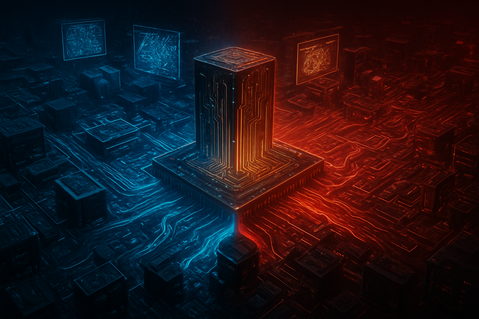
In a move that has sent shockwaves through the global semiconductor industry, the Chinese government has issued a series of directives instructing its leading technology firms to pause or significantly scale back orders for Nvidia’s latest high-performance chips, including the H200. This instruction, delivered by the Ministry of Industry and Information Technology (MIIT) and the Cyberspace Administration of China (CAC), marks a decisive escalation in the tech-cold war, signaling Beijing’s intent to achieve complete "silicon sovereignty" by 2030.
The immediate significance of this development cannot be overstated. By targeting the H200—the very hardware that powers the current frontier of generative AI—China is effectively imposing a domestic "security review" barrier on American high-end silicon. This policy forces domestic giants like Alibaba (NYSE: BABA) and Baidu (NASDAQ: BIDU) to shift their compute infrastructure toward homegrown alternatives, even at the cost of immediate performance parity, fundamentally altering the competitive landscape for artificial intelligence.
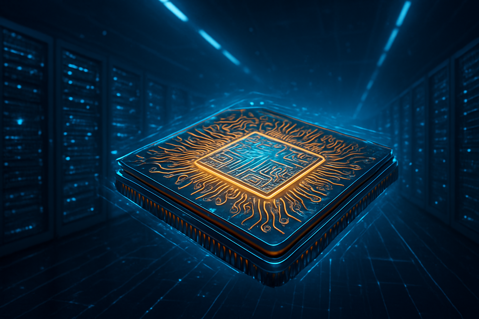
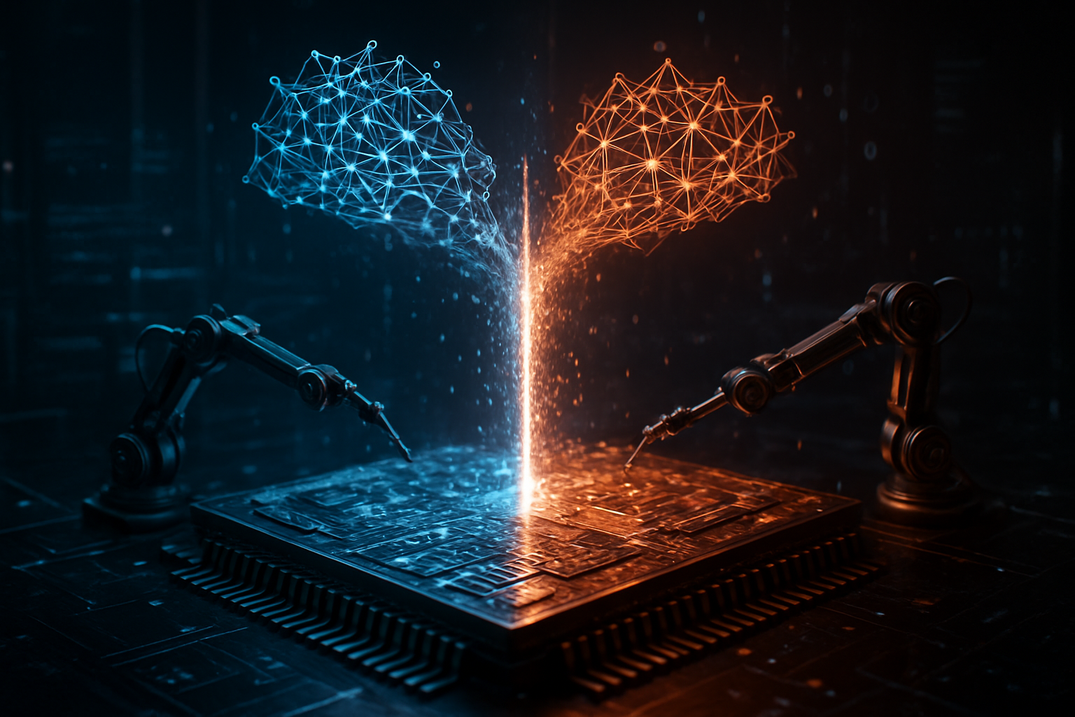
The Technical Stand-off: H200 vs. The Ascend 910C
The directive specifically targets the Nvidia (NASDAQ: NVDA) H200 and its China-compliant variants, which were designed to navigate the complex web of U.S. export controls. Technically, the H200 represented a bridge for Chinese firms to maintain access to HBM3e (high-bandwidth memory) architecture, essential for training large language models (LLMs). However, Chinese regulators have cited concerns over "backdoor" vulnerabilities and the potential for U.S. authorities to track compute workloads, prompting a comprehensive security audit that effectively halts new shipments.
In its place, Beijing is aggressively promoting the Huawei Ascend 910C. As of February 2026, technical benchmarks suggest the 910C has reached approximately 60% of the inference performance of Nvidia’s flagship H100, while reportedly surpassing Nvidia’s "Blackwell-lite" B20 in specific training scenarios. This indigenous hardware is backed by "Big Fund 3.0," a $47 billion investment vehicle designed to bridge the gap in manufacturing processes. While Huawei still struggles with yield rates compared to global standards, the government’s mandate—requiring data centers to source 50% of their chips locally—has provided a guaranteed market for these developing architectures.
Industry experts note that this transition is not without friction. The "Software Moat" established by Nvidia’s CUDA platform remains the primary technical hurdle for Chinese developers. To combat this, the MIIT has launched a national initiative to standardize a domestic software stack that allows for seamless porting of AI models from CUDA to Huawei’s CANN or Cambricon’s proprietary environments. Initial reactions from the research community are mixed, with some scientists warning that "fragmenting the global compute pool" could slow the overall pace of AI discovery while others see it as a necessary catalyst for diversified hardware innovation.
Competitive Fallout and the "Trump Surcharge"
The financial implications for Western tech giants are profound. Analysts report that Nvidia’s market share in China’s AI chip sector has collapsed from 66% in late 2024 to just 8% as of early 2026. This decline has been exacerbated by the "Trump Surcharge"—a 25% revenue-sharing fee introduced by the U.S. administration in late 2025 on all high-end semiconductor sales to China. For Nvidia, this essentially created a double-bind: pricing their products out of the market while facing an increasingly hostile regulatory environment in Beijing.
Beyond Nvidia, the competitive shift benefits domestic Chinese players such as Cambricon and Biren Technology, the latter of which reached a $12 billion valuation following its 2026 public listing. Conversely, major U.S.-aligned manufacturers like TSMC (NYSE: TSM) and Samsung (KRX: 005930) are finding themselves caught in the middle. While TSMC’s Arizona "Fab 21" has been a resounding success—reaching 92% yields on 4nm and 5nm processes—the loss of Chinese demand for advanced packaging (CoWoS) services is forcing these firms to pivot toward domestic U.S. and European clients.
For AI labs, this creates a split-market reality. Western labs like OpenAI and Anthropic continue to scale using unrestricted H200 and Blackwell clusters, while Chinese labs at Tencent and ByteDance are becoming the "world’s testbeds" for non-Nvidia hardware. This bifurcation could lead to a permanent divergence in AI model optimization, where Western models are optimized for raw memory bandwidth and Chinese models are engineered for the specific throughput characteristics of the Ascend 910C.
The Broader AI Landscape: The New "Iron Curtain"
This development is the clearest evidence yet of a growing "Iron Curtain" in the AI sector. The instruction to pause Nvidia orders fits perfectly into the broader narrative of the U.S. CHIPS Act, which has prioritized "reshoring" critical manufacturing. As of early 2026, the U.S. strategy has shifted from merely denying China access to high-end chips to actively incentivizing the relocation of the entire supply chain—from silicon ingots to advanced packaging—onto American soil.
The geopolitical impact is essentially a "forced decoupling." While the U.S. focuses on reshoring projects like the Micron (NASDAQ: MU) Idaho facility and the TSMC Arizona expansion, China is doubling down on its "National AI Compute Network." This initiative seeks to treat computing power like a public utility, much like water or electricity, ensuring that domestic firms have access to "good enough" compute without the threat of external sanctions.
However, concerns remain regarding the "efficiency gap." By isolating its tech ecosystem, China risks creating a "Galapagos effect," where its technology evolves in a specialized but ultimately limited direction. Comparing this to previous milestones, such as the 2017 "Sputnik moment" when China released its AI development plan, the 2026 directive represents the shift from planning to total execution. The global AI landscape is no longer a single, interconnected community of researchers, but two distinct silos competing for technological supremacy.
Future Developments: Toward 2028 and Beyond
Looking ahead, experts predict that the next major battleground will be in the realm of advanced packaging. While China has made strides in chip design, it remains reliant on external sources for the complex 2.5D and 3D packaging required for HBM3e integration. In response, a joint U.S.-Taiwan trade agreement signed in January 2026 aims to reshore these "back-end" facilities to the U.S. by 2028, further tightening the noose on China’s access to high-end manufacturing.
In the near term, expect to see Chinese "shadow orders" for Nvidia hardware through third-party nations decrease as the domestic security audits become more stringent. Instead, the industry will watch for the release of the Huawei Ascend 920 series, rumored for late 2026, which aims to achieve true performance parity with Western chips. The primary challenge for Beijing will be maintaining the energy efficiency of these domestic chips, as their current 7nm-class processes are significantly more power-hungry than the 3nm processes used by Nvidia’s latest generations.
A New Era of AI Competition
The directive to pause Nvidia H200 orders marks the end of the "Globalized AI" era and the beginning of "Sovereign AI." The significance of this moment in AI history is comparable to the initial export bans of 2022, but with a critical difference: this time, the restriction is coming from the buyer, not the seller. China is betting that short-term pain in compute performance will lead to long-term strategic independence.
The key takeaway is that the AI race is no longer just about who has the best algorithms, but who controls the supply chain from the sand to the server. For Nvidia, this represents a permanent loss of its most lucrative growth market. For the U.S., it is a validation of the "small yard, high fence" policy. In the coming months, watch for how Alibaba and Baidu adjust their AI roadmaps and whether the domestic Chinese hardware can truly support the massive compute requirements of the next generation of "Super-AGI" models.
This content is intended for informational purposes only and represents analysis of current AI developments.
TokenRing AI delivers enterprise-grade solutions for multi-agent AI workflow orchestration, AI-powered development tools, and seamless remote collaboration platforms.
For more information, visit https://www.tokenring.ai/.