Tag: In-Memory Computing

  • Breaking the Memory Wall: d-Matrix Secures $275M to Revolutionize AI Inference with In-Memory Computing

    Breaking the Memory Wall: d-Matrix Secures $275M to Revolutionize AI Inference with In-Memory Computing

    In a move that signals a paradigm shift in the semiconductor industry, AI chip pioneer d-Matrix announced on November 12, 2025, that it has successfully closed a $275 million Series C funding round. This massive infusion of capital, valuing the company at $2 billion, arrives at a critical juncture as the industry moves from the training phase of generative AI to the massive-scale deployment of inference. By leveraging its proprietary Digital In-Memory Computing (DIMC) architecture, d-Matrix aims to dismantle the "memory wall"—the physical bottleneck that has long hampered the performance and energy efficiency of traditional GPU-based systems.

    The significance of this development cannot be overstated. As large language models (LLMs) and agentic AI systems become integrated into the core workflows of global enterprises, the demand for low-latency, cost-effective inference has skyrocketed. While established players like NVIDIA (NASDAQ: NVDA) have dominated the training landscape, d-Matrix is positioning its "Corsair" and "Raptor" architectures as the specialized engines required for the next era of AI, where speed and power efficiency are the primary metrics of success.

    The End of the Von Neumann Bottleneck: Corsair and Raptor Architectures

    At the heart of d-Matrix's technological breakthrough is a fundamental departure from the traditional Von Neumann architecture. In standard chips, data must constantly travel between separate memory units (such as HBM) and processing units, creating a "memory wall" where the processor spends more time waiting for data than actually computing. d-Matrix solves this by embedding processing logic directly into the SRAM bit cells. This "Digital In-Memory Computing" (DIMC) approach allows the chip to perform calculations exactly where the data resides, achieving a staggering on-chip bandwidth of 150 TB/s—far exceeding the 4–8 TB/s offered by the latest HBM4 solutions.

    The company’s current flagship, the Corsair architecture, is already in mass production on the TSMC (NYSE: TSM) 6-nm process. Corsair is specifically optimized for small-batch LLM inference, capable of delivering 30,000 tokens per second on models like Llama 70B with a latency of just 2ms per token. This represents a 10x performance leap and a 3-to-5x improvement in energy efficiency compared to traditional GPU clusters. Unlike analog in-memory computing, which often suffers from noise and accuracy degradation, d-Matrix’s digital approach maintains the high precision required for enterprise-grade AI.

    Looking ahead, the company has also unveiled its next-generation Raptor architecture, slated for a 2026 commercial debut. Raptor will utilize a 4-nm process and introduce "3DIMC"—a 3D-stacked DRAM technology validated through the company’s Pavehawk test silicon. By stacking memory vertically on compute chiplets, Raptor aims to provide the massive memory capacity needed for complex "reasoning" models and multi-agent systems, further extending d-Matrix's lead in the inference market.

    Strategic Positioning and the Battle for the Data Center

    The $275 million Series C round was co-led by Bullhound Capital, Triatomic Capital, and Temasek, with participation from major institutional players including the Qatar Investment Authority (QIA) and M12, the venture fund of Microsoft (NASDAQ: MSFT). This diverse group of backers underscores the global strategic importance of d-Matrix’s technology. For hyperscalers like Microsoft, Amazon (NASDAQ: AMZN), and Alphabet (NASDAQ: GOOGL), reducing the Total Cost of Ownership (TCO) for AI inference is a top priority. By adopting d-Matrix’s DIMC chips, these tech giants can significantly reduce their data center power consumption and floor space requirements.

    The competitive implications for NVIDIA are profound. While NVIDIA’s H100 and B200 GPUs remain the gold standard for training, their reliance on expensive and power-hungry High Bandwidth Memory (HBM) makes them less efficient for high-volume inference tasks. d-Matrix is carving out a specialized niche that could potentially disrupt the dominance of general-purpose GPUs in the inference market. Furthermore, the modular, chiplet-based design of the Corsair platform allows for high manufacturing yields and faster iteration cycles, giving d-Matrix a tactical advantage in a rapidly evolving hardware landscape.

    A Broader Shift in the AI Landscape

    The rise of d-Matrix reflects a broader trend toward specialized AI hardware. In the early days of the generative AI boom, the industry relied on brute-force scaling. Today, the focus has shifted toward efficiency and sustainability. The "memory wall" was once a theoretical problem discussed in academic papers; now, it is a multi-billion-dollar hurdle for the global economy. By overcoming this bottleneck, d-Matrix is enabling the "Age of AI Inference," where AI models can run locally and instantaneously without the massive energy overhead of current cloud infrastructures.

    This development also addresses growing concerns regarding the environmental impact of AI. As data centers consume an increasing share of the world's electricity, the 5x energy efficiency offered by DIMC technology could be a deciding factor for regulators and ESG-conscious corporations. d-Matrix’s success serves as a proof of concept for non-Von Neumann computing, potentially paving the way for other breakthroughs in neuromorphic and optical computing that seek to further blur the line between memory and processing.

    The Road Ahead: Agentic AI and 3D Stacking

    As d-Matrix moves into 2026, the focus will shift from the successful rollout of Corsair to the scaling of the Raptor platform. The industry is currently moving toward "agentic AI"—systems that don't just generate text but perform multi-step tasks and reasoning. These workloads require even more memory capacity and lower latency than current LLMs. The 3D-stacked DRAM in the Raptor architecture is designed specifically for these high-complexity tasks, positioning d-Matrix at the forefront of the next wave of AI capabilities.

    However, challenges remain. d-Matrix must continue to expand its software stack to ensure seamless integration with popular frameworks like PyTorch and TensorFlow. Furthermore, as competitors like Cerebras and Groq also vie for the inference crown, d-Matrix will need to leverage its new capital to rapidly scale its global operations, particularly in its R&D hubs in Bangalore, Sydney, and Toronto. Experts predict that the next 18 months will be a "land grab" for inference market share, with d-Matrix currently holding a significant architectural lead.

    Summary and Final Assessment

    The $275 million Series C funding of d-Matrix marks a pivotal moment in the evolution of AI hardware. By successfully commercializing Digital In-Memory Computing through its Corsair architecture and setting a roadmap for 3D-stacked memory with Raptor, d-Matrix has provided a viable solution to the memory wall that has limited the industry for decades. The backing of major sovereign wealth funds and tech giant venture arms like Microsoft’s M12 suggests that the industry is ready to move beyond the GPU-centric model for inference.

    As we look toward 2026, d-Matrix stands as a testament to the power of architectural innovation. While the "training wars" were won by high-bandwidth GPUs, the "inference wars" will likely be won by those who can process data where it lives. For the tech industry, the message is clear: the future of AI isn't just about more compute; it's about smarter, more integrated memory.


    This content is intended for informational purposes only and represents analysis of current AI developments.

    TokenRing AI delivers enterprise-grade solutions for multi-agent AI workflow orchestration, AI-powered development tools, and seamless remote collaboration platforms.
    For more information, visit https://www.tokenring.ai/.

  • The Silicon Brain: How Next-Gen AI Chips Are Rewriting the Future of Intelligence

    The Silicon Brain: How Next-Gen AI Chips Are Rewriting the Future of Intelligence

    The artificial intelligence revolution, once primarily a software-driven phenomenon, is now being fundamentally reshaped by a parallel transformation in hardware. As traditional processors hit their architectural limits, a new era of AI chip architecture is dawning. This shift is characterized by innovative designs and specialized accelerators that promise to unlock unprecedented AI capabilities with immediate and profound impact, moving beyond the general-purpose computing paradigms that have long dominated the tech landscape. These advancements are not just making AI faster; they are making it smarter, more efficient, and capable of operating in ways previously thought impossible, signaling a critical juncture in the development of artificial intelligence.

    Unpacking the Architectural Revolution: Specialized Silicon for a Smarter Future

    The future of AI chip architecture is rapidly evolving, driven by the increasing demand for computational power, energy efficiency, and real-time processing required by complex AI models. This evolution is moving beyond traditional CPU and GPU architectures towards specialized accelerators and innovative designs, with the global AI hardware market projected to reach $210.50 billion by 2034. Experts believe that the next phase of AI breakthroughs will be defined by hardware innovation, not solely by larger software models, prioritizing faster, more efficient, and scalable chips, often adopting multi-component, heterogeneous systems where each component is engineered for a specific function within a single package.

    At the forefront of this revolution are groundbreaking designs that fundamentally rethink how computation and memory interact. Neuromorphic computing, for instance, draws inspiration from the human brain, utilizing "spiking neural networks" (SNNs) to process information. Unlike traditional processors that execute instructions sequentially or in parallel with predefined instructions, these chips are event-driven, activating only when new information is detected, much like biological neurons communicate through discrete electrical spikes. This brain-inspired approach, exemplified by Intel (NASDAQ: INTC)'s Hala Point, which uses over 1,000 Loihi 2 processors, offers exceptional energy efficiency, real-time processing, and adaptability, enabling AI to learn dynamically on the device. Initial prototypes have shown performing AI workloads 50 times faster and using 100 times less energy than conventional systems.

    Another significant innovation is In-Memory Computing (IMC), which directly tackles the "von Neumann bottleneck"—the inefficiency caused by data constantly shuffling between the processor and separate memory units. IMC integrates computation directly within or adjacent to memory units, drastically reducing data transfer delays and power consumption. This approach is particularly promising for large AI models and compact edge devices, offering significant improvements in AI costs, reduced compute time, and lower power usage, especially for inference applications. Complementing this, 3D Stacking (or 3D packaging) involves vertically integrating multiple semiconductor dies. This allows for massive and fast data movement by shortening interconnect distances, bypassing bottlenecks inherent in flat, 2D designs, and offering substantial improvements in performance and energy efficiency. Companies like AMD (NASDAQ: AMD) with its 3D V-Cache and Intel (NASDAQ: INTC) with Foveros technology are already implementing these advancements, with early prototypes demonstrating performance gains of roughly an order of magnitude over comparable 2D chips.

    These innovative designs are coupled with a new generation of specialized AI accelerators. While Graphics Processing Units (GPUs) from NVIDIA (NASDAQ: NVDA) were revolutionary for parallel AI workloads, dedicated AI chips are taking specialization to the next level. Neural Processing Units (NPUs) are specifically engineered from the ground up for neural network computations, delivering superior performance and energy efficiency, especially for edge computing. Google (NASDAQ: GOOGL)'s Tensor Processing Units (TPUs) are a prime example of custom Application-Specific Integrated Circuits (ASICs), meticulously designed for machine learning tasks. TPUs, now in their seventh generation (Ironwood), feature systolic array architectures and high-bandwidth memory (HBM), capable of performing 16K multiply-accumulate operations per cycle in their latest versions, significantly accelerating AI workloads across Google services. Custom ASICs offer the highest level of optimization, often delivering 10 to 100 times greater energy efficiency compared to GPUs for specific AI tasks, although they come with less flexibility and higher initial design costs. The AI research community and industry experts widely acknowledge the critical role of this specialized hardware, recognizing that future AI breakthroughs will increasingly depend on such infrastructure, not solely on software advancements.

    Reshaping the Corporate Landscape: Who Wins in the AI Silicon Race?

    The advent of advanced AI chip architectures is profoundly impacting the competitive landscape across AI companies, tech giants, and startups, driving a strategic shift towards vertical integration and specialized solutions. This silicon arms race is poised to redefine market leadership and disrupt existing product and service offerings.

    Tech giants are strategically positioned to benefit immensely due to their vast resources and established ecosystems. Companies like Google (NASDAQ: GOOGL), Amazon (NASDAQ: AMZN), Microsoft (NASDAQ: MSFT), and Meta (NASDAQ: META) are heavily investing in developing their own custom AI silicon. Google's TPUs, Amazon Web Services (AWS)'s Trainium and Inferentia chips, Microsoft's Azure Maia 100 and Azure Cobalt 100, and Meta's MTIA are all examples of this vertical integration strategy. By designing their own chips, these companies aim to optimize performance for specific workloads, reduce reliance on third-party suppliers like NVIDIA (NASDAQ: NVDA), and achieve significant cost efficiencies, particularly for AI inference tasks. This move allows them to differentiate their cloud offerings and internal AI services, gaining tighter control over their hardware and software stacks.

    The competitive implications for major AI labs and tech companies are substantial. There's a clear trend towards reduced dependence on NVIDIA's dominant GPUs, especially for AI inference, where custom ASICs can offer lower power consumption and cost. This doesn't mean NVIDIA is out of the game; they continue to lead the AI training market and are exploring advanced packaging like 3D stacking and silicon photonics. However, the rise of custom silicon forces NVIDIA and AMD (NASDAQ: AMD), which is expanding its AI capabilities with products like the MI300 series, to innovate rapidly and offer more specialized, high-performance solutions. The ability to offer AI solutions with superior energy efficiency and lower latency will be a key differentiator, with neuromorphic and in-memory computing excelling in this regard, particularly for edge devices where power constraints are critical.

    This architectural shift also brings potential disruption to existing products and services. The enhanced efficiency of neuromorphic computing, in-memory computing, and NPUs enables more powerful AI processing directly on devices, reducing the need for constant cloud connectivity. This could disrupt cloud-based AI service models, especially for real-time, privacy-sensitive, or low-power applications. Conversely, it could also lead to the democratization of AI, lowering the barrier to entry for AI development by making sophisticated AI systems more accessible and cost-effective. The focus will shift from general-purpose computing to workload-specific optimization, with systems integrating multiple processor types (GPUs, CPUs, NPUs, TPUs) for different tasks, potentially disrupting traditional hardware sales models.

    For startups, this specialized landscape presents both challenges and opportunities. Startups focused on niche hardware or specific AI applications can thrive by providing highly optimized solutions that fill gaps left by general-purpose hardware. For instance, neuromorphic computing startups like BrainChip, Rain Neuromorphics, and GrAI Matter Labs are developing energy-efficient chips for edge AI, robotics, and smart sensors. Similarly, in-memory computing startups like TensorChip and Axelera AI are creating chips for high throughput and low latency at the edge. Semiconductor foundries like TSMC (NYSE: TSM) and Samsung (KRX: 005930), along with IP providers like Marvell (NASDAQ: MRVL) and Broadcom (NASDAQ: AVGO), are crucial enablers, providing the advanced manufacturing and design expertise necessary for these complex architectures. Their mastery of 3D stacking and other advanced packaging techniques will make them essential partners and leaders in delivering the next generation of high-performance AI chips.

    A Broader Canvas: AI Chips and the Future of Society

    The future of AI chip architecture is not just a technical evolution; it's a societal one, deeply intertwined with the broader AI landscape and trends. These advancements are poised to enable unprecedented levels of performance, efficiency, and capability, promising profound impacts across society and various industries, while also presenting significant concerns that demand careful consideration.

    These advanced chip architectures directly address the escalating computational demands and inefficiencies of modern AI. The "memory wall" in traditional von Neumann architectures and the skyrocketing energy costs of training large AI models are major concerns that specialized chips are designed to overcome. The shift towards these architectures signifies a move towards more pervasive, responsive, and efficient intelligence, enabling the proliferation of AI at the "edge"—on devices like IoT sensors, smartphones, and autonomous vehicles—where real-time processing, low power consumption, and data security are paramount. This decentralization of AI capabilities is a significant trend, comparable to the shift from mainframes to personal computing or the rise of cloud computing, democratizing access to powerful computational resources.

    The impacts on society and industries are expected to be transformative. In healthcare, faster and more accurate AI processing will enable early disease diagnosis, personalized medicine, and accessible telemedicine. Autonomous vehicles, drones, and advanced robotics will benefit from real-time decision-making, enhancing safety and efficiency. Cybersecurity will see neuromorphic chips continuously learning from network traffic patterns to detect new and evolving threats with low latency. In manufacturing, advanced robots and optimized industrial processes will become more adaptable and efficient. For consumer electronics, supercomputer-level performance could be integrated into compact devices, powering highly responsive AI assistants and advanced functionalities. Crucially, improved efficiency and reduced power consumption in data centers will be critical for scaling AI operations, leading to lower operational costs and potentially making AI solutions more accessible to developers with limited resources.

    Despite the immense potential, the future of AI chip architecture raises several critical concerns. While newer architectures aim for significant energy efficiency, the sheer scale of AI development still demands immense computational resources, contributing to a growing carbon footprint and straining power grids. This raises ethical questions about the environmental impact and the perpetuation of societal inequalities if AI development is not powered by renewable sources or if biased models are deployed. Ensuring ethical AI development requires addressing issues like data quality, fairness, and the potential for algorithmic bias. The increased processing of sensitive data at the edge also raises privacy concerns that must be managed through secure enclaves and robust data protection. Furthermore, the high cost of developing and deploying high-performance AI accelerators could create a digital divide, although advancements in AI-driven chip design could eventually reduce costs. Other challenges include thermal management for densely packed 3D-stacked chips, the need for new software compatibility and development frameworks, and the rapid iteration of hardware contributing to e-waste.

    This architectural evolution is as significant as, if not more profound than, previous AI milestones. The initial AI revolution was fueled by the adaptation of GPUs, overcoming the limitations of general-purpose CPUs. The current emergence of specialized hardware, neuromorphic designs, and in-memory computing moves beyond simply shrinking transistors, fundamentally re-architecting how AI operates. This enables improvements in performance and efficiency that are orders of magnitude greater than what traditional scaling could achieve alone, with some comparing the leap in performance to an improvement equivalent to 26 years of Moore's Law-driven CPU advancements for AI tasks. This represents a decentralization of intelligence, making AI more ubiquitous and integrated into our physical environment.

    The Horizon: What's Next for AI Silicon?

    The relentless pursuit of speed, efficiency, and specialization continues to drive the future developments in AI chip architecture, promising to unlock new frontiers in artificial intelligence. Both near-term enhancements and long-term revolutionary paradigms are on the horizon, addressing current limitations and enabling unprecedented applications.

    In the near term (next 1-5 years), advancements will focus on enhancing existing technologies through sophisticated integration methods. Advanced packaging and heterogeneous integration will become the norm, moving towards modular, chiplet-based architectures. Companies like NVIDIA (NASDAQ: NVDA) with its Blackwell architecture, AMD (NASDAQ: AMD) with its MI300 series, and hyperscalers like Google (NASDAQ: GOOGL) with TPU v6 and Amazon (NASDAQ: AMZN) with Trainium 2 are already leveraging multi-die GPU modules and High-Bandwidth Memory (HBM) to achieve exponential gains. Research indicates that these 3D chips can significantly outperform 2D chips, potentially leading to 100- to 1,000-fold improvements in energy-delay product. Specialized accelerators (ASICs and NPUs) will become even more prevalent, with a continued focus on energy efficiency through optimized power consumption features and specialized circuit designs, crucial for both data centers and edge devices.

    Looking further ahead into the long term (beyond 5 years), revolutionary computing paradigms are being explored to overcome the fundamental limits of silicon-based electronics. Optical computing, which uses light (photons) instead of electricity, promises extreme processing speed, reduced energy consumption, and high parallelism, particularly well-suited for the linear algebra operations central to AI. Hybrid architectures combining photonic accelerators with digital processors are expected to become mainstream over the next decade, with the optical processors market forecasted to reach US$3 billion by 2034. Neuromorphic computing will continue to evolve, aiming for ultra-low-power AI systems capable of continuous learning and adaptation, fundamentally moving beyond the traditional Von Neumann architecture bottlenecks. The most speculative, yet potentially transformative, development lies in Quantum AI Chips. By leveraging quantum-mechanical phenomena, these chips hold immense promise for accelerating machine learning, optimization, and simulation tasks that are intractable for classical computers. The convergence of AI chips and quantum computing is expected to lead to breakthroughs in areas like drug discovery, climate modeling, and cybersecurity, with the quantum optical computer market projected to reach US$300 million by 2034.

    These advanced architectures will unlock a new generation of sophisticated AI applications. Even larger and more complex Large Language Models (LLMs) and generative AI models will be trained and inferred, leading to more human-like text generation and advanced content creation. Autonomous systems (self-driving cars, robotics, drones) will benefit from real-time decision-making, object recognition, and navigation powered by specialized edge AI chips. The proliferation of Edge AI will enable sophisticated AI capabilities directly on smartphones and IoT devices, supporting applications like facial recognition and augmented reality. Furthermore, High-Performance Computing (HPC) and scientific research will be accelerated, impacting fields such as drug discovery and climate modeling.

    However, significant challenges must be addressed. Manufacturing complexity and cost for advanced semiconductors, especially at smaller process nodes, remain immense. The projected power consumption and heat generation of next-generation AI chips, potentially exceeding 15,000 watts per unit by 2035, demand fundamental changes in data center infrastructure and cooling systems. The memory wall and energy associated with data movement continue to be major hurdles, with optical interconnects being explored as a solution. Software integration and development frameworks for novel architectures like optical and quantum computing are still nascent. For quantum AI chips, qubit fragility, short coherence times, and scalability issues are significant technical hurdles. Experts predict a future shaped by hybrid architectures, combining the strengths of different computing paradigms, and foresee AI itself becoming instrumental in designing and optimizing future chips. While NVIDIA (NASDAQ: NVDA) is expected to maintain its dominance in the medium term, competition from AMD (NASDAQ: AMD) and custom ASICs will intensify, with optical computing anticipated to become a mainstream solution for data centers by 2027/2028.

    The Dawn of Specialized Intelligence: A Concluding Assessment

    The ongoing transformation in AI chip architecture marks a pivotal moment in the history of artificial intelligence, heralding a future where specialized, highly efficient, and increasingly brain-inspired designs are the norm. The key takeaway is a definitive shift away from the general-purpose computing paradigms that once constrained AI's potential. This architectural revolution is not merely an incremental improvement but a fundamental reshaping of how AI is built and deployed, promising to unlock unprecedented capabilities and integrate intelligence seamlessly into our world.

    This development's significance in AI history cannot be overstated. Just as the adaptation of GPUs catalyzed the deep learning revolution, the current wave of specialized accelerators, neuromorphic computing, and advanced packaging techniques is enabling the training and deployment of AI models that were once computationally intractable. This hardware innovation is the indispensable backbone of modern AI breakthroughs, from advanced natural language processing to computer vision and autonomous systems, making real-time, intelligent decision-making possible across various industries. Without these purpose-built chips, sophisticated AI algorithms would remain largely theoretical, making this architectural shift fundamental to AI's practical realization and continued progress.

    The long-term impact will be transformative, leading to ubiquitous and pervasive AI embedded into nearly every device and system, from tiny IoT sensors to advanced robotics. This will enable enhanced automation and new capabilities across healthcare, manufacturing, finance, and automotive, fostering decentralized intelligence and hybrid AI infrastructures. However, this future also necessitates a rethinking of data center design and sustainability, as the rising power demands of next-gen AI chips will require fundamental changes in infrastructure and cooling. The geopolitical landscape around semiconductor manufacturing will also continue to be a critical factor, influencing chip availability and market dynamics.

    In the coming weeks and months, watch for continuous advancements in chip efficiency and novel architectures, particularly in neuromorphic computing and heterogeneous integration. The emergence of specialized chips for generative AI and LLMs at the edge will be a critical indicator of future capabilities, enabling more natural and private user experiences. Keep an eye on new software tools and platforms that simplify the deployment of complex AI models on these specialized chipsets, as their usability will be key to widespread adoption. The competitive landscape among established semiconductor giants and innovative AI hardware startups will continue to drive rapid advancements, especially in HBM-centric computing and thermal management solutions. Finally, monitor the evolving global supply chain dynamics and the trend of shifting AI model training to "thick edge" servers, as these will directly influence the pace and direction of AI hardware development. The future of AI is undeniably intertwined with the future of its underlying silicon, promising an era of specialized intelligence that will redefine our technological capabilities.


    This content is intended for informational purposes only and represents analysis of current AI developments.

    TokenRing AI delivers enterprise-grade solutions for multi-agent AI workflow orchestration, AI-powered development tools, and seamless remote collaboration platforms.
    For more information, visit https://www.tokenring.ai/.

  • Silicon’s New Frontier: AI Semiconductor Startups Ignite a Revolution with Breakthrough Designs

    Silicon’s New Frontier: AI Semiconductor Startups Ignite a Revolution with Breakthrough Designs

    The artificial intelligence landscape is witnessing a profound and rapid transformation, driven by a new generation of semiconductor startups that are challenging the established order. These agile innovators are not merely refining existing chip architectures; they are fundamentally rethinking how AI computation is performed, delivering groundbreaking designs and highly specialized solutions that are immediately significant for the burgeoning AI industry. With the insatiable demand for AI computing infrastructure showing no signs of slowing, these emerging players are crucial for unlocking unprecedented levels of performance and efficiency, pushing the boundaries of what AI can achieve.

    At the heart of this disruption are companies pioneering diverse architectural innovations, from leveraging light for processing to integrating computation directly into memory. Their efforts are directly addressing critical bottlenecks, such as the "memory wall" and the escalating energy consumption of AI, thereby making AI systems more efficient, accessible, and cost-effective. This wave of specialized silicon is enabling industries across the board—from healthcare and finance to manufacturing and autonomous systems—to deploy AI at various scales, fundamentally reshaping how we interact with technology and accelerating the entire innovation cycle within the semiconductor industry.

    Detailed Technical Coverage: A New Era of AI Hardware

    The advancements from these emerging AI semiconductor startups are characterized by a departure from traditional von Neumann architectures, focusing instead on specialized designs to overcome inherent limitations and meet the escalating demands of AI.

    Leading the charge in photonic supercomputing are companies like Lightmatter and Celestial AI. Lightmatter's Passage platform, a 3D-stacked silicon photonics engine, utilizes light to process information, promising incredible bandwidth density and the ability to connect millions of processors at the speed of light. This directly combats the bottlenecks of traditional electronic systems, which are limited by electrical resistance and heat generation. Celestial AI's Photonic Fabric similarly aims to reinvent data movement within AI systems, addressing the interconnect bottleneck by providing ultra-fast, low-latency optical links. Unlike electrical traces, optical connections can achieve massive throughput with significantly reduced energy consumption, a critical factor for large-scale AI data centers. Salience Labs, a spin-out from Oxford University, is developing a hybrid photonic-electronic chip that combines an ultra-high-speed multi-chip processor with standard electronics, claiming to deliver "massively parallel processing performance within a given power envelope" and exceeding the speed and power limitations of purely electronic systems. Initial reactions to these photonic innovations are highly positive, with significant investor interest and partnerships indicating strong industry validation for their potential to speed up AI processing and reduce energy footprints.

    In the realm of in-memory computing (IMC), startups like d-Matrix and EnCharge AI are making significant strides. d-Matrix is building chips for data center AI inference using digital IMC techniques, embedding compute cores alongside memory to drastically reduce memory bottlenecks. This "first-of-its-kind" compute platform relies on chiplet-based processors, making generative AI applications more commercially viable by integrating computation directly into memory. EnCharge AI has developed charge-based IMC technology, originating from DARPA-funded R&D, with test chips reportedly achieving over 150 TOPS/W for 8-bit compute—the highest reported efficiency to date. This "beyond-digital accelerator" approach offers orders-of-magnitude higher compute efficiency and density than even other optical or analog computing concepts, critical for power-constrained edge applications. Axelera AI is also revolutionizing edge AI with a hardware and software platform integrating proprietary IMC technology with a RISC-V-based dataflow architecture, accelerating computer vision by processing visual data directly within memory. These IMC innovations fundamentally alter the traditional von Neumann architecture, promising significant reductions in latency and power consumption for data-intensive AI workloads.

    For specialized LLM and edge accelerators, companies like Cerebras Systems, Groq, SiMa.ai, and Hailo are delivering purpose-built hardware. Cerebras Systems, known for its wafer-scale chips, builds what it calls the world's fastest AI accelerators. Its latest WSE-3 (Wafer-Scale Engine 3), announced in March 2024, features 4 trillion transistors and 900,000 AI cores, leveraging [TSM:TSM] (Taiwan Semiconductor Manufacturing Company) 5nm process. This single, massive chip eliminates latency and power consumption associated with data movement between discrete chips, offering unprecedented on-chip memory and bandwidth crucial for large, sparse AI models like LLMs. Groq develops ultra-fast AI inference hardware, specifically a Language Processing Unit (LPU), with a unique architecture designed for predictable, low-latency inference in real-time interactive AI applications, often outperforming GPUs in specific LLM tasks. On the edge, SiMa.ai delivers a software-first machine learning system-on-chip (SoC) platform, the Modalix chip family, claiming 10x performance-per-watt improvements over existing solutions for edge AI. Hailo, with its Hailo-10 chip, similarly focuses on low-power AI processing optimized for Generative AI (GenAI) workloads in devices like PCs and smart vehicles, enabling complex GenAI models to run locally. These specialized chips represent a significant departure from general-purpose GPUs, offering tailored efficiency for the specific computational patterns of LLMs and the stringent power requirements of edge devices.

    Impact on AI Companies, Tech Giants, and Startups

    The rise of these innovative AI semiconductor startups is sending ripples across the entire tech industry, fundamentally altering competitive landscapes and strategic advantages for established AI companies, tech giants, and other emerging ventures.

    Major tech giants like [GOOG] (Google), [INTC] (Intel), [AMD] (Advanced Micro Devices), and [NVDA] (NVIDIA) stand to both benefit and face significant competitive pressures. While NVIDIA currently holds a dominant market share in AI GPUs, its position is increasingly challenged by both established players and these agile startups. Intel's Gaudi accelerators and AMD's Instinct GPUs are directly competing, particularly in inference workloads, by offering cost-effective alternatives. However, the truly disruptive potential lies with startups pioneering photonic and in-memory computing, which directly address the memory and power bottlenecks that even advanced GPUs encounter, potentially offering superior performance per watt for specific AI tasks. Hyperscalers like Google and [AMZN] (Amazon) are also increasingly developing custom AI chips for their own data centers (e.g., Google's TPUs), reducing reliance on external vendors and optimizing performance for their specific workloads, a trend that poses a long-term disruption to traditional chip providers.

    The competitive implications extend to all major AI labs and tech companies. The shift from general-purpose to specialized hardware means that companies relying on less optimized solutions for demanding AI tasks risk being outmaneuvered. The superior energy efficiency offered by photonic and in-memory computing presents a critical competitive advantage, as AI workloads consume a significant and growing portion of data center energy. Companies that can deploy more sustainable and cost-effective AI infrastructure will gain a strategic edge. Furthermore, the democratization of advanced AI through specialized LLM and edge accelerators can make sophisticated AI capabilities more accessible and affordable, potentially disrupting business models that depend on expensive, centralized AI infrastructure by enabling more localized and cost-effective deployments.

    For startups, this dynamic environment creates both opportunities and challenges. AI startups focused on software or specific AI applications will benefit from the increased accessibility and affordability of high-performance AI hardware, lowering operational costs and accelerating development cycles. However, the high costs of semiconductor R&D and manufacturing mean that only well-funded or strategically partnered startups can truly compete in the hardware space. Emerging AI semiconductor startups gain strategic advantages by focusing on highly specialized niches where traditional architectures are suboptimal, offering significant performance and power efficiency gains for specific AI workloads. Established companies, in turn, leverage their extensive ecosystems, manufacturing capabilities, and market reach, often acquiring or partnering with promising startups to integrate innovative hardware with their robust software platforms and cloud services. The global AI chip market, projected to reach over $232.85 billion by 2034, ensures intense competition and a continuous drive for innovation, with a strong emphasis on specialized, energy-efficient chips.

    Wider Significance: Reshaping the AI Ecosystem

    These innovations in AI semiconductors are not merely technical improvements; they represent a foundational shift in how AI is designed, deployed, and scaled, profoundly impacting the broader AI landscape and global technological trends.

    This new wave of semiconductor innovation fits into a broader AI landscape characterized by a symbiotic relationship where AI's rapid growth drives demand for more efficient semiconductors, while advancements in chip technology enable breakthroughs in AI capabilities. This creates a "self-improving loop" where AI is becoming an "active co-creator" of the very hardware that drives it. The increasing sophistication of AI algorithms, particularly large deep learning models, demands immense computational power and energy efficiency. Traditional hardware struggles to handle these workloads without excessive power consumption or heat. These new semiconductor designs are directly aimed at mitigating these challenges, offering solutions that are orders of magnitude more efficient than general-purpose processors. The rise of edge AI, in particular, signifies a critical shift from cloud-bound AI to pervasive, on-device intelligence, spreading AI capabilities across networks and enabling real-time, localized decision-making.

    The overall impacts of these advancements are far-reaching. Economically, the integration of AI is expected to significantly boost the semiconductor industry, with projections of the global AI chip market exceeding $150 billion in 2025 and potentially reaching $400 billion by 2027. This growth will foster new industries and job creation across various sectors, from healthcare and automotive to manufacturing and defense. Transformative applications include advanced diagnostics, autonomous vehicles, predictive maintenance, and smarter consumer electronics. Furthermore, edge AI's ability to enable real-time, low-power processing on devices has the potential to improve accessibility to advanced technology, particularly in underserved regions, making AI more scalable and ubiquitous. Crucially, the focus on energy efficiency in chip design and manufacturing is vital for minimizing AI's environmental footprint, addressing the significant energy and water consumption associated with chip production and large-scale AI models.

    However, this transformative potential comes with significant concerns. The high costs and complexity of designing and manufacturing advanced semiconductors (fabs can cost up to $20 billion) and cutting-edge equipment (over $150 million for EUV lithography machines) create significant barriers. Technical complexities, such as managing heat dissipation and ensuring reliability at nanometer scales, remain formidable. Supply chain vulnerabilities and geopolitical tensions, particularly given the reliance on concentrated manufacturing hubs, pose significant risks. While new designs aim for efficiency, the sheer scale of AI models means overall energy demand continues to surge, with data centers potentially tripling power consumption by 2030. Data security and privacy also present challenges, particularly with sensitive data processed on numerous distributed edge devices. Moreover, integrating new AI systems often requires significant hardware and software modifications, and many semiconductor companies struggle to monetize software effectively.

    This current period marks a distinct and pivotal phase in AI history, differentiating itself from earlier milestones. In previous AI breakthroughs, semiconductors primarily served as an enabler. Today, AI is an active co-creator of the hardware itself, fundamentally reshaping chip design and manufacturing processes. The transition to pervasive, on-device intelligence signifies a maturation of AI from a theoretical capability to practical, ubiquitous deployment. This era also actively pushes beyond Moore's Law, exploring new compute methodologies like photonic and in-memory computing to deliver step-change improvements in speed and energy efficiency that go beyond traditional transistor scaling.

    Future Developments: The Road Ahead for AI Hardware

    The trajectory of AI semiconductor innovation points towards a future characterized by hybrid architectures, ubiquitous AI, and an intensified focus on neuromorphic computing, even as significant challenges remain.

    In the near term, we can expect to see a continued proliferation of hybrid chip architectures, integrating novel materials and specialized functions alongside traditional silicon logic. Advanced packaging and chiplet architectures will be critical, allowing for modular designs, faster iteration, and customization, directly addressing the "memory wall" by integrating compute and memory more closely. AI itself will become an increasingly vital tool in the semiconductor industry, automating tasks like layout optimization, error detection, yield optimization, predictive maintenance, and accelerating verification processes, thereby reducing design cycles and costs. On-chip optical communication, particularly through silicon photonics, will see increased adoption to improve efficiency and reduce bottlenecks.

    Looking further ahead, neuromorphic computing, which designs chips to mimic the human brain's neural structure, will become more prevalent, improving energy efficiency and processing for AI tasks, especially in edge and IoT applications. The long-term vision includes fully integrated chips built entirely from beyond-silicon materials or advanced superconducting circuits for quantum computing and ultra-low-power edge AI devices. These advancements will enable ubiquitous AI, with miniaturization and efficiency gains allowing AI to be embedded in an even wider array of devices, from smart dust to advanced medical implants. Potential applications include enhanced autonomous systems, pervasive edge AI and IoT, significantly more efficient cloud computing and data centers, and transformative capabilities in healthcare and scientific research.

    However, several challenges must be addressed for these future developments to fully materialize. The immense costs of manufacturing and R&D for advanced semiconductor fabs (up to $20 billion) and cutting-edge equipment (over $150 million for EUV lithography machines) create significant barriers. Technical complexities, such as managing heat dissipation and ensuring reliability at nanometer scales, remain formidable. Supply chain vulnerabilities and geopolitical risks also loom large, particularly given the reliance on concentrated manufacturing hubs. The escalating energy consumption of AI models, despite efficiency gains, presents a sustainability challenge that requires ongoing innovation.

    Experts predict a sustained "AI Supercycle," driven by the relentless demand for AI capabilities, with the AI chip market potentially reaching $500 billion by 2028. There will be continued diversification and specialization of AI hardware, optimizing specific material combinations and architectures for particular AI workloads. Cloud providers and large tech companies will increasingly engage in vertical integration, designing their own custom silicon. A significant shift towards inference-specific hardware is also anticipated, as generative AI applications become more widespread, favoring specialized hardware due to lower cost, higher energy efficiency, and better performance for highly specialized tasks. While an "AI bubble" is a concern for some financial analysts due to extreme valuations, the fundamental technological shifts underpin a transformative era for AI hardware.

    Comprehensive Wrap-up: A New Dawn for AI Hardware

    The emerging AI semiconductor startup scene is a vibrant hotbed of innovation, signifying a pivotal moment in the history of artificial intelligence. These companies are not just improving existing technologies; they are spearheading a paradigm shift towards highly specialized, energy-efficient, and fundamentally new computing architectures.

    The key takeaways from this revolution are clear: specialization is paramount, with chips tailored for specific AI workloads like LLMs and edge devices; novel computing paradigms such as photonic supercomputing and in-memory computing are directly addressing the "memory wall" and energy bottlenecks; and a "software-first" approach is becoming crucial for seamless integration and developer adoption. This intense innovation is fueled by significant venture capital investment, reflecting the immense economic potential and strategic importance of advanced AI hardware.

    This development holds profound significance in AI history. It marks a transition from AI being merely an enabler of technology to becoming an active co-creator of the very hardware that drives it. By democratizing and diversifying the hardware landscape, these startups are enabling new AI capabilities and fostering a more sustainable future for AI by relentlessly pursuing energy efficiency. This era is pushing beyond the traditional limits of Moore's Law, exploring entirely new compute methodologies.

    The long-term impact will be a future where AI is pervasive and seamlessly integrated into every facet of our lives, from autonomous systems to smart medical implants. The availability of highly efficient and specialized chips will drive the development of new AI algorithms and models, leading to breakthroughs in real-time multimodal AI and truly autonomous systems. While cloud computing will remain essential, powerful edge AI accelerators could lead to a rebalancing of compute resources, improving privacy, latency, and resilience. This "wild west" environment will undoubtedly lead to the emergence of new industry leaders and solidify energy efficiency as a central design principle for all future computing hardware.

    In the coming weeks and months, several key indicators will reveal the trajectory of this revolution. Watch for significant funding rounds and strategic partnerships between startups and larger tech companies, which signal market validation and scalability. New chip and accelerator releases, particularly those demonstrating substantial performance-per-watt improvements or novel capabilities for LLMs and edge devices, will be crucial. Pay close attention to the commercialization and adoption of photonic supercomputing from companies like Lightmatter and Celestial AI, and the widespread deployment of in-memory computing chips from startups like EnCharge AI. The maturity of software ecosystems and development tools for these novel hardware solutions will be paramount for their success. Finally, anticipate consolidation through mergers and acquisitions as the market matures, with larger tech companies integrating promising startups into their portfolios. This vibrant and rapidly evolving landscape promises to redefine the future of artificial intelligence.


    This content is intended for informational purposes only and represents analysis of current AI developments.

    TokenRing AI delivers enterprise-grade solutions for multi-agent AI workflow orchestration, AI-powered development tools, and seamless remote collaboration platforms.
    For more information, visit https://www.tokenring.ai/.

  • AI Chips Unleashed: The 2025 Revolution in Brain-Inspired Designs, Optical Speed, and Modular Manufacturing

    AI Chips Unleashed: The 2025 Revolution in Brain-Inspired Designs, Optical Speed, and Modular Manufacturing

    November 2025 marks an unprecedented surge in AI chip innovation, characterized by the commercialization of brain-like computing, a leap into light-speed processing, and a manufacturing paradigm shift towards modularity and AI-driven efficiency. These breakthroughs are immediately reshaping the technological landscape, driving sustainable, powerful AI from the cloud to the farthest edge of the network.

    The artificial intelligence hardware sector is currently undergoing a profound transformation, with significant advancements in both chip design and manufacturing processes directly addressing the escalating demands for performance, energy efficiency, and scalability. The immediate significance of these developments lies in their capacity to accelerate AI deployment across industries, drastically reduce its environmental footprint, and enable a new generation of intelligent applications that were previously out of reach due to computational or power constraints.

    Technical Deep Dive: The Engines of Tomorrow's AI

    The core of this revolution lies in several distinct yet interconnected technical advancements. Neuromorphic computing, which mimics the human brain's neural architecture, is finally moving beyond theoretical research into practical, commercial applications. Chips like Intel's (NASDAQ: INTC) Hala Point system, BrainChip's (ASX: BRN) Akida Pulsar, and Innatera's Spiking Neural Processor (SNP), have seen significant advancements or commercial launches in 2025. These systems are inherently energy-efficient, offering low-latency solutions ideal for edge AI, robotics, and the Internet of Things (IoT). For instance, Akida Pulsar boasts up to 500 times lower energy consumption and 100 times latency reduction compared to conventional AI cores for real-time, event-driven processing at the edge. Furthermore, USC researchers have demonstrated artificial neurons that replicate biological function with significantly reduced chip size and energy consumption, promising to advance artificial general intelligence. This paradigm shift directly addresses the critical need for sustainable AI by drastically cutting power usage in resource-constrained environments.

    Another major bottleneck in traditional computing architectures, the "memory wall," is being shattered by in-memory computing (IMC) and processing-in-memory (PIM) chips. These innovative designs perform computations directly within memory, dramatically reducing the movement of data between the processor and memory. This reduction in data transfer, in turn, slashes power consumption and significantly boosts processing speed. Companies like Qualcomm (NASDAQ: QCOM) are integrating near-memory computing into new solutions such as the AI250, providing a generational leap in effective memory bandwidth and efficiency specifically for AI inference workloads. This technology is crucial for managing the massive data processing demands of complex AI algorithms, enabling faster and more efficient training and inference for burgeoning generative AI models and large language models (LLMs).

    Perhaps one of the most futuristic developments is the emergence of optical computing. Scientists at Tsinghua University have achieved a significant milestone by developing a light-powered AI chip, OFE², capable of handling data at an unprecedented 12.5 GHz. This optical computing breakthrough completes complex pattern-recognition tasks by directing light beams through on-chip structures, consuming significantly less energy than traditional electronic devices. This innovation offers a potent solution to the growing energy demands of AI, potentially freeing AI from being a major contributor to global energy shortages. It promises a new generation of real-time, ultra-low-energy AI, crucial for sustainable and widespread deployment across various sectors.

    Finally, as traditional transistor scaling (often referred to as Moore's Law) faces physical limits, advanced packaging technologies and chiplet architectures have become paramount. Technologies like 2.5D and 3D stacking (e.g., CoWoS, 3DIC), Fan-Out Panel-Level Packaging (FO-PLP), and hybrid bonding are crucial for boosting performance, increasing integration density, improving signal integrity, and enhancing thermal management for AI chips. Complementing this, chiplet technology, which involves modularizing chip functions into discrete components, is gaining significant traction, with the Universal Chiplet Interconnect Express (UCIe) standard expanding its adoption. These innovations are the new frontier for hardware optimization, offering flexibility, cost-effectiveness, and faster development cycles. They also mitigate supply chain risks by allowing manufacturers to source different parts from multiple suppliers. The market for advanced packaging is projected to grow eightfold by 2033, underscoring its immediate importance for the widespread adoption of AI chips into consumer devices and automotive applications.

    Competitive Landscape: Winners and Disruptors

    These advancements are creating clear winners and potential disruptors within the AI industry. Chip designers and manufacturers at the forefront of these innovations stand to benefit immensely. Intel, with its neuromorphic Hala Point system, and BrainChip, with its Akida Pulsar, are well-positioned in the energy-efficient edge AI market. Qualcomm's integration of near-memory computing in its AI250 strengthens its leadership in mobile and edge AI processing. NVIDIA (NASDAQ: NVDA), while not explicitly mentioned for neuromorphic or optical chips, continues to dominate the high-performance computing space for AI training and is a key enabler for AI-driven manufacturing.

    The competitive implications are significant. Major AI labs and tech companies reliant on traditional architectures will face pressure to adapt or risk falling behind in performance and energy efficiency. Companies that can rapidly integrate these new chip designs into their products and services will gain a substantial strategic advantage. For instance, the ability to deploy AI models with significantly lower power consumption opens up new markets in battery-powered devices, remote sensing, and pervasive AI. The modularity offered by chiplets could also democratize chip design to some extent, allowing smaller players to combine specialized chiplets from various vendors to create custom, high-performance AI solutions, potentially disrupting the vertically integrated chip design model.

    Furthermore, AI's role in optimizing its own creation is a game-changer. AI-driven Electronic Design Automation (EDA) tools are dramatically accelerating chip design timelines—for example, reducing a 5nm chip's optimization cycle from six months to just six weeks. This means faster time-to-market for new AI chips, improved design quality, and more efficient, higher-yield manufacturing processes. Samsung (KRX: 005930), for instance, is establishing an "AI Megafactory" powered by 50,000 NVIDIA GPUs to revolutionize its chip production, integrating AI throughout its entire manufacturing flow. Similarly, SK Group is building an "AI factory" in South Korea with NVIDIA, focusing on next-generation memory and autonomous fab digital twins to optimize efficiency. These efforts are critical for meeting the skyrocketing demand for AI-optimized semiconductors and bolstering supply chain resilience amidst geopolitical shifts.

    Broader Significance: Shaping the AI Future

    These innovations fit perfectly into the broader AI landscape, addressing critical trends such as the insatiable demand for computational power for increasingly complex models (like LLMs), the push for sustainable and energy-efficient AI, and the proliferation of AI at the edge. The move towards neuromorphic and optical computing represents a fundamental shift away from the Von Neumann architecture, which has dominated computing for decades, towards more biologically inspired or physically optimized processing methods. This transition is not merely an incremental improvement but a foundational change that could unlock new capabilities in AI.

    The impacts are far-reaching. On one hand, these advancements promise more powerful, ubiquitous, and efficient AI, enabling breakthroughs in areas like personalized medicine, autonomous systems, and advanced scientific research. On the other hand, potential concerns, while mitigated by the focus on energy efficiency, still exist regarding the ethical implications of more powerful AI and the increasing complexity of hardware development. However, the current trajectory is largely positive, aiming to make AI more accessible and environmentally responsible.

    Comparing this to previous AI milestones, such as the rise of GPUs for deep learning or the development of specialized AI accelerators like Google's TPUs, these current advancements represent a diversification and deepening of the hardware foundation. While earlier milestones focused on brute-force parallelization, today's innovations are about architectural efficiency, novel physics, and self-optimization through AI, pushing beyond the limits of traditional silicon. This multi-pronged approach suggests a more robust and sustainable path for AI's continued growth.

    The Road Ahead: Future Developments and Challenges

    Looking to the near-term, we can expect to see further integration of these technologies. Hybrid chips combining neuromorphic, in-memory, and conventional processing units will likely become more common, optimizing specific workloads for maximum efficiency. The UCIe standard for chiplets will continue to gain traction, leading to a more modular and customizable AI hardware ecosystem. In the long-term, the full potential of optical computing, particularly in areas requiring ultra-high bandwidth and low latency, could revolutionize data centers and telecommunications infrastructure, creating entirely new classes of AI applications.

    Potential applications on the horizon include highly sophisticated, real-time edge AI for autonomous vehicles that can process vast sensor data with minimal latency and power, advanced robotics capable of learning and adapting in complex environments, and medical devices that can perform on-device diagnostics with unprecedented accuracy and speed. Generative AI and LLMs will also see significant performance boosts, enabling more complex and nuanced interactions, and potentially leading to more human-like AI capabilities.

    However, challenges remain. Scaling these nascent technologies to mass production while maintaining cost-effectiveness is a significant hurdle. The development of robust software ecosystems and programming models that can fully leverage the unique architectures of neuromorphic and optical chips will be crucial. Furthermore, ensuring interoperability between diverse chiplet designs and maintaining supply chain stability amidst global economic fluctuations will require continued innovation and international collaboration. Experts predict a continued convergence of hardware and software co-design, with AI playing an ever-increasing role in optimizing its own underlying infrastructure.

    A New Era for AI Hardware

    In summary, the latest innovations in AI chip design and manufacturing—encompassing neuromorphic computing, in-memory processing, optical chips, advanced packaging, and AI-driven manufacturing—represent a pivotal moment in the history of artificial intelligence. These breakthroughs are not merely incremental improvements but fundamental shifts that promise to make AI more powerful, energy-efficient, and ubiquitous than ever before.

    The significance of these developments cannot be overstated. They are addressing the core challenges of AI scalability and sustainability, paving the way for a future where AI is seamlessly integrated into every facet of our lives, from smart cities to personalized health. As we move forward, the interplay between novel chip architectures, advanced manufacturing techniques, and AI's self-optimizing capabilities will be critical to watch. The coming weeks and months will undoubtedly bring further announcements and demonstrations as companies race to capitalize on these transformative technologies, solidifying this period as a new era for AI hardware.


    This content is intended for informational purposes only and represents analysis of current AI developments.

    TokenRing AI delivers enterprise-grade solutions for multi-agent AI workflow orchestration, AI-powered development tools, and seamless remote collaboration platforms.
    For more information, visit https://www.tokenring.ai/.

  • Beyond Silicon: A New Era of Semiconductor Innovation Dawns

    Beyond Silicon: A New Era of Semiconductor Innovation Dawns

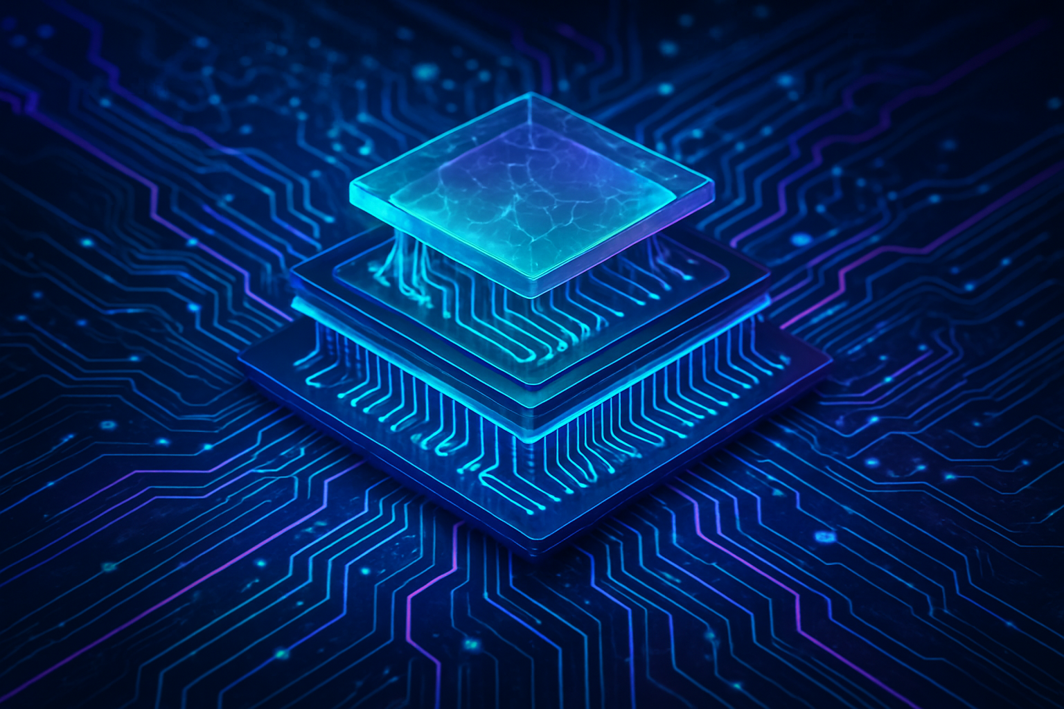
    The foundational bedrock of the digital age, silicon, is encountering its inherent physical limits, prompting a monumental shift in the semiconductor industry. A new wave of materials and revolutionary chip architectures is emerging, promising to redefine the future of computing and propel artificial intelligence (AI) into unprecedented territories. This paradigm shift extends far beyond the advancements seen in wide bandgap (WBG) materials like silicon carbide (SiC) and gallium nitride (GaN), ushering in an era of ultra-efficient, high-performance, and highly specialized processing capabilities essential for the escalating demands of AI, high-performance computing (HPC), and pervasive edge intelligence.

    This pivotal moment is driven by the relentless pursuit of greater computational power, energy efficiency, and miniaturization, all while confronting the economic and physical constraints of traditional silicon scaling. The innovations span novel two-dimensional (2D) materials, ferroelectrics, and ultra-wide bandgap (UWBG) semiconductors, coupled with groundbreaking architectural designs such as 3D chiplets, neuromorphic computing, in-memory processing, and photonic AI chips. These developments are not merely incremental improvements but represent a fundamental re-imagining of how data is processed, stored, and moved, promising to sustain technological progress well beyond the traditional confines of Moore's Law and power the next generation of AI-driven applications.

    Technical Revolution: Unpacking the Next-Gen Chip Blueprint

    The technical advancements pushing the semiconductor frontier are multifaceted, encompassing both revolutionary materials and ingenious architectural designs. At the material level, researchers are exploring Two-Dimensional (2D) Materials like graphene, molybdenum disulfide (MoS₂), and indium selenide (InSe). While graphene boasts exceptional electrical conductivity, its lack of an intrinsic bandgap has historically limited its direct use in digital switching. However, recent breakthroughs in fabricating semiconducting graphene on silicon carbide substrates are demonstrating useful bandgaps and electron mobilities ten times greater than silicon. MoS₂ and InSe, ultrathin at just a few atoms thick, offer superior electrostatic control, tunable bandgaps, and high carrier mobility, crucial for scaling transistors below the 10-nanometer mark where silicon faces insurmountable physical limitations. InSe, in particular, shows promise for up to a 50% reduction in power consumption compared to projected silicon performance.

    Beyond 2D materials, Ferroelectric Materials are poised to revolutionize memory technology, especially for ultra-low power applications in both traditional and neuromorphic computing. By integrating ferroelectric capacitors (FeCAPs) with memristors, these materials enable highly efficient dual-use architectures for AI training and inference, which are critical for the development of ultra-low power edge AI devices. Furthermore, Ultra-Wide Bandgap (UWBG) Semiconductors such as diamond, gallium oxide (Ga₂O₃), and aluminum nitride (AlN) are being explored. These materials possess even larger bandgaps than current WBG materials, offering orders of magnitude improvement in figures of merit for power and radio frequency (RF) electronics, leading to higher operating voltages, switching frequencies, and significantly reduced losses, enabling more compact and lightweight system designs.

    Complementing these material innovations are radical shifts in chip architecture. 3D Chip Architectures and Advanced Packaging (Chiplets) are moving away from monolithic processors. Instead, different functional blocks are manufactured separately—often using diverse, optimal processes—and then integrated into a single package. Techniques like 3D stacking and Intel's (NASDAQ: INTC) Foveros allow for increased density, performance, and flexibility, enabling heterogeneous designs where different components can be optimized for specific tasks. This modular approach is vital for high-performance computing (HPC) and AI accelerators. Neuromorphic Computing, inspired by the human brain, integrates memory and processing to minimize data movement, offering ultra-low power consumption and high-speed processing for complex AI tasks, making them ideal for embedded AI in IoT devices and robotics.

    Furthermore, In-Memory Computing / Near-Memory Computing aims to overcome the "memory wall" bottleneck by performing computations directly within or very close to memory units, drastically increasing speed and reducing power consumption for data-intensive AI workloads. Photonic AI Chips / Silicon Photonics integrate optical components onto silicon, using light instead of electrons for signal processing. This offers potentially 1,000 times greater energy efficiency than traditional electronic GPUs for specific high-speed, low-power AI tasks, addressing the massive power consumption of modern data centers. While still nascent, Quantum Computing Architectures, with their hybrid quantum-classical designs and cryogenic CMOS chips, promise unparalleled processing power for intractable AI algorithms. Initial reactions from the AI research community and industry experts are largely enthusiastic, recognizing these advancements as indispensable for continuing the trajectory of technological progress in an era of increasingly complex and data-hungry AI.

    Industry Ripples: Reshaping the AI Competitive Landscape

    The advent of these advanced semiconductor technologies and novel chip architectures is poised to profoundly reshape the competitive landscape for AI companies, tech giants, and nimble startups alike. A discernible "AI chip arms race" is already underway, creating a foundational economic shift where superior hardware increasingly dictates AI capabilities and market leadership.

    Tech giants, particularly hyperscale cloud providers, are at the forefront of this transformation, heavily investing in custom silicon development. Companies like Alphabet's Google (NASDAQ: GOOGL) with its Tensor Processing Units (TPUs) and Axion processors, Microsoft (NASDAQ: MSFT) with Maia 100 and Cobalt 100, Amazon (NASDAQ: AMZN) with Trainium and Inferentia, and Meta Platforms (NASDAQ: META) with MTIA are all designing Application-Specific Integrated Circuits (ASICs) optimized for their colossal cloud AI workloads. This strategic vertical integration reduces their reliance on external suppliers like NVIDIA (NASDAQ: NVDA), mitigates supply chain risks, and enables them to offer differentiated, highly efficient AI services. NVIDIA itself, with its dominant CUDA ecosystem and new Blackwell architecture, along with Taiwan Semiconductor Manufacturing Company (TSMC) (NYSE: TSM) and its technological leadership in advanced manufacturing processes (e.g., 2nm Gate-All-Around FETs and Extreme Ultraviolet lithography), continue to be primary beneficiaries and market leaders, setting the pace for innovation.

    For AI companies, these advancements translate into enhanced performance and efficiency, enabling the development of more powerful and energy-efficient AI models. Specialized chips allow for faster training and inference, crucial for complex deep learning and real-time AI applications. The ability to diversify and customize hardware solutions for specific AI tasks—such as natural language processing or computer vision—will become a significant competitive differentiator. This scalability ensures that as AI models grow in complexity and data demands, the underlying hardware can keep pace without significant performance degradation, while also addressing environmental concerns through improved energy efficiency.

    Startups, while facing the immense cost and complexity of developing chips on bleeding-edge process nodes (often exceeding $100 million for some designs), can still find significant opportunities. Cloud-based design tools and AI-driven Electronic Design Automation (EDA) are lowering barriers to entry, allowing smaller players to access advanced resources and accelerate chip development. This enables startups to focus on niche solutions, such as specialized AI accelerators for edge computing, neuromorphic computing, in-memory processing, or photonic AI chips, potentially disrupting established players with innovative, high-performance, and energy-efficient designs that can be brought to market faster. However, the high capital expenditure required for advanced chip development also risks consolidating power among companies with deeper pockets and strong foundry relationships. The industry is moving beyond general-purpose computing towards highly specialized designs optimized for AI workloads, challenging the dominance of traditional GPU providers and fostering an ecosystem of custom accelerators and open-source alternatives.

    A New Foundation for the AI Supercycle: Broader Implications

    The emergence of these advanced semiconductor technologies signifies a fundamental re-architecture of computing that extends far beyond mere incremental improvements. It represents a critical response to the escalating demands of the "AI Supercycle," particularly the insatiable computational and energy requirements of generative AI and large language models (LLMs). These innovations are not just supporting the current AI revolution but are laying the groundwork for its next generation, fitting squarely into the broader trend of specialized, energy-efficient, and highly parallelized computing.

    One of the most profound impacts is the direct assault on the von Neumann bottleneck, the traditional architectural limitation where data movement between separate processing and memory units creates significant delays and consumes vast amounts of energy. Technologies like In-Memory Computing (IMC) and neuromorphic computing fundamentally bypass this bottleneck by integrating processing directly within or very close to memory, or by mimicking the brain's parallel, memory-centric processing. This architectural shift promises orders of magnitude improvements in both speed and energy efficiency, vital for training and deploying ever-larger and more complex AI models. Similarly, photonic chips, which use light instead of electricity for computation and data transfer, offer unprecedented speed and energy efficiency, drastically reducing the thermal footprint of data centers—a growing environmental concern.

    The wider significance also lies in enabling pervasive Edge AI and IoT. The ultra-low power consumption and real-time processing capabilities of analog AI chips and neuromorphic systems are indispensable for deploying AI autonomously on devices ranging from smartphones and wearables to advanced robotics and autonomous vehicles. This decentralization of AI processing reduces latency, conserves bandwidth, and enhances privacy by keeping data local. Furthermore, the push for energy efficiency across these new materials and architectures is a crucial step towards more sustainable AI, addressing the substantial and growing electricity consumption of global computing infrastructure.

    Compared to previous AI milestones, such as the development of deep learning or the transformer architecture, which were primarily algorithmic and software-driven, these semiconductor advancements represent a fundamental shift in hardware paradigms. While software breakthroughs showed what AI could achieve, these hardware innovations are determining how efficiently, scalably, and sustainably it can be achieved, and even what new kinds of AI can emerge. They are enabling new computational models that move beyond decades of traditional computing design, breaking physical limitations inherent in electrical signals, and redefining the possible for real-time, ultra-low power, and potentially quantum-enhanced AI. This symbiotic relationship, where AI's growth drives hardware innovation and hardware, in turn, unlocks new AI capabilities, is a hallmark of this era.

    However, this transformative period is not without its concerns. Many of these technologies are still in nascent stages, facing significant challenges in manufacturability, reliability, and scaling. The integration of diverse new components, such as photonic and electronic elements, into existing systems, and the establishment of industry-wide standards, present complex hurdles. The software ecosystems for many emerging hardware types, particularly analog and neuromorphic chips, are still maturing, making programming and widespread adoption challenging. The immense R&D costs associated with designing and manufacturing advanced semiconductors also risk concentrating innovation among a few dominant players. Furthermore, while many technologies aim for efficiency, the manufacturing processes for advanced packaging, for instance, can be more energy-intensive, raising questions about the overall environmental footprint. As AI becomes more powerful and ubiquitous through these hardware advancements, ethical considerations surrounding privacy, bias, and potential misuse of AI technologies will become even more pressing.

    The Horizon: Anticipating Future Developments and Applications

    The trajectory of semiconductor innovation points towards a future where AI capabilities are continually amplified by breakthroughs in materials science and chip architectures. In the near term (1-5 years), we can expect significant advancements in the integration of 2D materials like graphene and MoS₂ into novel processing hardware, particularly through monolithic 3D integration that promises reduced processing time, power consumption, latency, and footprint for AI computing. Some 2D materials are already demonstrating the potential for up to a 50% reduction in power consumption compared to silicon's projected performance by 2037. Spintronics, leveraging electron spin, will become crucial for developing faster and more energy-efficient non-volatile memory systems, with breakthroughs in materials like thulium iron garnet (TmIG) films enabling greener magnetic random-access memory (MRAM) for data centers. Furthermore, specialized neuromorphic and analog AI accelerators will see wider deployment, bringing energy-efficient, localized AI to smart homes, industrial IoT, and personalized health applications, while silicon photonics will enhance on-chip communication for faster, more efficient AI chips in data centers.

    Looking further into the long term (5+ years), the landscape becomes even more transformative. Continued research into 2D materials aims for full integration of all functional layers onto a single chip, leading to unprecedented compactness and efficiency. The vision of all-optical and analog optical computing will move closer to reality, eliminating electrical conversions for significantly reduced power consumption and higher bandwidth, enabling deep neural network computations entirely in the optical domain. Spintronics will further advance brain-inspired computing models, efficiently emulating neurons and synapses in hardware for spiking and convolutional neural networks with novel data storage and processing. While nascent, the integration of quantum computing with semiconductors will progress, with hybrid quantum-classical architectures tackling complex AI algorithms beyond classical capabilities. Alongside these, novel memory technologies like resistive random-access memory (RRAM) and phase-change memory (PCM) will become pivotal for advanced neuromorphic and in-memory computing systems.

    These advancements will unlock a plethora of potential applications. Ultra-low-power Edge AI will become ubiquitous, enabling real-time, local processing on smartphones, IoT sensors, autonomous vehicles, and wearables without constant cloud connectivity. High-Performance Computing and Data Centers will see their colossal energy demands significantly reduced by faster, more energy-efficient memory and optical processing, accelerating training and inference for even the most complex generative AI models. Neuromorphic and bio-inspired AI systems, powered by spintronic and 2D material chips, will mimic the human brain's efficiency for complex pattern recognition and unsupervised learning. Advanced robotics, autonomous systems, and even scientific discovery in fields like astronomy and personalized medicine will be supercharged by the massive computational power these technologies afford.

    However, significant challenges remain. The integration complexity of novel optical, 2D, and spintronic components with existing electronic hardware poses formidable technical hurdles. Manufacturing costs and scalability for cutting-edge semiconductor processes remain high, requiring substantial investment. Material science and fabrication techniques for novel materials need further refinement to ensure reliability and quality control. Balancing the drive for energy efficiency with the ever-increasing demand for computational power is a constant tightrope walk. A lack of standardization and ecosystem development could hinder widespread adoption, while the persistent global talent shortage in the semiconductor industry could impede progress. Finally, efficient thermal management will remain critical as devices become even more densely integrated.

    Expert predictions paint a future where AI and semiconductor innovation share a symbiotic relationship. AI will not just consume advanced chips but will actively participate in their creation, optimizing design, layout, and quality control, accelerating the innovation cycle itself. The focus will shift from raw performance to application-specific efficiency, driving the development of highly customized chips for diverse AI workloads. Memory innovation, including High Bandwidth Memory (HBM) and next-generation DRAM alongside novel spintronic and 2D material-based solutions, will continue to meet AI's insatiable data hunger. Experts foresee ubiquitous Edge AI becoming pervasive, making AI more accessible and scalable across industries. The global AI chip market is projected to surpass $150 billion in 2025 and could reach an astonishing $1.3 trillion by 2030, underscoring the profound economic impact. Ultimately, sustainability will emerge as a key driving force, pushing the industry towards energy-efficient designs, novel materials, and refined manufacturing processes to reduce the environmental footprint of AI. The co-optimization across the entire hardware-software stack will become crucial, marking a new era of integrated innovation.

    The Next Frontier: A Hardware Renaissance for AI

    The semiconductor industry is currently undergoing a profound and unprecedented transformation, driven by the escalating computational demands of artificial intelligence. This "hardware renaissance" extends far beyond the traditional confines of silicon scaling and even established wide bandgap materials, embracing novel materials, advanced packaging techniques, and entirely new computing paradigms to deliver the speed, energy efficiency, and scalability required by modern AI.

    Key takeaways from this evolution include the definitive move into a post-silicon era, where the physical and economic limitations of traditional silicon are being overcome by new materials like 2D semiconductors, ferroelectrics, and advanced UWBG materials. Efficiency is paramount, with the primary motivations for these emerging technologies centered on achieving unprecedented power and energy efficiency, particularly crucial for the training and inference of large AI models. A central focus is the memory-compute convergence, aiming to overcome the "memory wall" bottleneck through innovations in in-memory computing and neuromorphic designs that tightly integrate processing and data storage. This is complemented by modular and heterogeneous design facilitated by advanced packaging techniques, allowing diverse, specialized components (chiplets) to be integrated into single, high-performance packages.

    This period represents a pivotal moment in AI history, fundamentally redefining the capabilities and potential of Artificial Intelligence. These advancements are not merely incremental; they are enabling a new class of AI hardware capable of processing vast datasets with unparalleled efficiency, unlocking novel computing paradigms, and accelerating AI development from hyperscale data centers to the furthest edge devices. The immediate significance lies in overcoming the physical limitations that have begun to constrain traditional silicon-based chips, ensuring that the exponential growth of AI can continue unabated. This era signifies that AI has transitioned from largely theoretical research into an age of massive practical deployment, demanding a commensurate leap in computational infrastructure. Furthermore, AI itself is becoming a symbiotic partner in this evolution, actively participating in optimizing chip design, layout, and manufacturing processes, creating an "AI supercycle" where AI consumes advanced chips and also aids in their creation.

    The long-term impact of these emerging semiconductor technologies on AI will be transformative and far-reaching, paving the way for ubiquitous AI seamlessly integrated into every facet of daily life and industry. This will contribute to sustained economic growth, with AI projected to add approximately $13 trillion to the global economy by 2030. The shift towards brain-inspired computing, in-memory processing, and optical computing could fundamentally redefine computational power, energy efficiency, and problem-solving capabilities, pushing the boundaries of what AI can achieve. Crucially, these more efficient materials and computing paradigms will be vital in addressing the sustainability imperative as AI's energy footprint continues to grow. Finally, the pursuit of novel materials and domestic semiconductor supply chains will continue to shape the geopolitical landscape, impacting global leadership in technology.

    In the coming weeks and months, industry watchers should keenly observe announcements from major chip manufacturers like Intel (NASDAQ: INTC), Advanced Micro Devices (NASDAQ: AMD), and NVIDIA (NASDAQ: NVDA) regarding their next-generation AI accelerators and product roadmaps, which will showcase the integration of these emerging technologies. Keep an eye on new strategic partnerships and investments between AI developers, research institutions, and semiconductor foundries, particularly those aimed at scaling novel material production and advanced packaging capabilities. Breakthroughs in manufacturing 2D semiconductor materials at scale for commercial integration could signal the true dawn of a "post-silicon era." Additionally, follow developments in neuromorphic and in-memory computing prototypes as they move from laboratories towards real-world applications, with in-memory chips anticipated for broader use within three to five years. Finally, observe how AI algorithms themselves are increasingly utilized to accelerate the discovery and design of new semiconductor materials, creating a virtuous cycle of innovation that promises to redefine the future of computing.


    This content is intended for informational purposes only and represents analysis of current AI developments.

    TokenRing AI delivers enterprise-grade solutions for multi-agent AI workflow orchestration, AI-powered development tools, and seamless remote collaboration platforms.
    For more information, visit https://www.tokenring.ai/.

  • Beyond the Silicon Ceiling: Next-Gen AI Chips Ignite a New Era of Intelligence

    Beyond the Silicon Ceiling: Next-Gen AI Chips Ignite a New Era of Intelligence

    The relentless pursuit of artificial general intelligence (AGI) and the explosive growth of large language models (LLMs) are pushing the boundaries of traditional computing, ushering in a transformative era for AI chip architectures. We are witnessing a profound shift beyond the conventional CPU and GPU paradigms, as innovators race to develop specialized, energy-efficient, and brain-inspired silicon designed to unlock unprecedented AI capabilities. This architectural revolution is not merely an incremental upgrade; it represents a foundational re-thinking of how AI processes information, promising to dismantle existing computational bottlenecks and pave the way for a future where intelligent systems are faster, more efficient, and ubiquitous.

    The immediate significance of these next-generation AI chips cannot be overstated. They are the bedrock upon which the next wave of AI innovation will be built, addressing critical challenges such as the escalating energy consumption of AI data centers, the "von Neumann bottleneck" that limits data throughput, and the demand for real-time, on-device AI in countless applications. From neuromorphic processors mimicking the human brain to optical chips harnessing the speed of light, these advancements are poised to accelerate AI development cycles, enable more complex and sophisticated AI models, and ultimately redefine the scope of what artificial intelligence can achieve across industries.

    A Deep Dive into Architectural Revolution: From Neurons to Photons

    The innovations driving next-generation AI chip architectures are diverse and fundamentally depart from the general-purpose designs that have dominated computing for decades. At their core, these new architectures aim to overcome the limitations of the von Neumann architecture—where processing and memory are separate, leading to significant energy and time costs for data movement—and to provide hyper-specialized efficiency for AI workloads.

    Neuromorphic Computing stands out as a brain-inspired paradigm. Chips like Intel's (NASDAQ: INTC) Loihi and IBM's TrueNorth utilize spiking neural networks (SNNs), mimicking biological neurons that communicate via electrical spikes. A key differentiator is their inherent integration of computation and memory, dramatically reducing the von Neumann bottleneck. These chips boast ultra-low power consumption, often operating at 1% to 10% of traditional processors' power draw, and excel in real-time processing, making them ideal for edge AI applications. For instance, Intel's Loihi 2 features 1 million neurons and 128 million synapses, offering significant improvements in energy efficiency and latency for event-driven, sparse AI workloads compared to conventional GPUs.

    In-Memory Computing (IMC) and Analog AI Accelerators represent another significant leap. IMC performs computations directly within or adjacent to memory, drastically cutting down data transfer overhead. This approach is particularly effective for the multiply-accumulate (MAC) operations central to deep learning. Analog AI accelerators often complement IMC by using analog circuits for computations, consuming significantly less energy than their digital counterparts. Innovations like ferroelectric field-effect transistors (FeFET) and phase-change memory are enhancing the efficiency and compactness of IMC solutions. For example, startups like Mythic and Cerebras Systems (private) are developing analog and wafer-scale engines, respectively, to push the boundaries of in-memory and near-memory computation, claiming orders of magnitude improvements in performance-per-watt for specific AI inference tasks. D-Matrix's 3D Digital In-Memory Compute (3DIMC) technology, for example, aims to offer superior speed and energy efficiency compared to traditional High Bandwidth Memory (HBM) for AI inference.

    Optical/Photonic AI Chips are perhaps the most revolutionary, leveraging light (photons) instead of electrons for processing. These chips promise machine learning tasks at the speed of light, potentially classifying wireless signals within nanoseconds—about 100 times faster than the best digital alternatives—while being significantly more energy-efficient and generating less heat. By encoding and processing data with light, photonic chips can perform key deep neural network computations entirely optically on-chip. Lightmatter (private) and Ayar Labs (private) are notable players in this emerging field, developing silicon photonics solutions that could revolutionize applications from 6G wireless systems to autonomous vehicles by enabling ultra-fast, low-latency AI inference directly at the source of data.

    Finally, Domain-Specific Architectures (DSAs), Application-Specific Integrated Circuits (ASICs), and Neural Processing Units (NPUs) represent a broader trend towards "hyper-specialized silicon." Unlike general-purpose CPUs/GPUs, DSAs are meticulously engineered for specific AI workloads, such as large language models, computer vision, or edge inference. Google's (NASDAQ: GOOGL) Tensor Processing Units (TPUs) are a prime example, optimized specifically for AI workloads in data centers, delivering unparalleled performance for tasks like TensorFlow model training. Similarly, Google's Coral NPUs are designed for energy-efficient on-device inference. These custom chips achieve higher performance and energy efficiency by shedding the overhead of general-purpose designs, providing a tailored fit for the unique computational patterns of AI.

    Initial reactions from the AI research community and industry experts are overwhelmingly positive, albeit with a healthy dose of realism regarding the challenges ahead. Many see these architectural shifts as not just necessary but inevitable for AI to continue its exponential growth. Experts highlight the potential for these chips to democratize advanced AI by making it more accessible and affordable, especially for resource-constrained applications. However, concerns remain about the complexity of developing software stacks for these novel architectures and the significant investment required for their commercialization and mass production.

    Industry Impact: Reshaping the AI Competitive Landscape

    The advent of next-generation AI chip architectures is poised to dramatically reshape the competitive landscape for AI companies, tech giants, and startups alike. This shift favors entities capable of deep hardware-software co-design and those willing to invest heavily in specialized silicon.

    NVIDIA (NASDAQ: NVDA), currently the undisputed leader in AI hardware with its dominant GPU accelerators, faces both opportunities and challenges. While NVIDIA continues to innovate with new GPU generations like Blackwell, incorporating features like transformer engines and greater memory bandwidth, the rise of highly specialized architectures could eventually erode its general-purpose AI supremacy for certain workloads. NVIDIA is proactively responding by investing in its own software ecosystem (CUDA) and developing more specialized solutions, but the sheer diversity of new architectures means competition will intensify.

    Tech giants like Google (NASDAQ: GOOGL), Amazon (NASDAQ: AMZN), and Microsoft (NASDAQ: MSFT) are significant beneficiaries, primarily through their massive cloud infrastructure and internal AI development. Google's TPUs have given it a strategic advantage in AI training for its own services and Google Cloud. Amazon's AWS has its own Inferentia and Trainium chips, and Microsoft is reportedly developing its own custom AI silicon. These companies leverage their vast resources to design chips optimized for their specific cloud workloads, reducing reliance on external vendors and gaining performance and cost efficiencies. This vertical integration allows them to offer more competitive AI services to their customers.

    Startups are a vibrant force in this new era, often focusing on niche architectural innovations that established players might overlook or find too risky. Companies like Cerebras Systems (private) with its wafer-scale engine, Mythic (private) with analog in-memory compute, Lightmatter (private) and Ayar Labs (private) with optical computing, and SambaNova Systems (private) with its reconfigurable dataflow architecture, are all aiming to disrupt the market. These startups, often backed by significant venture capital, are pushing the boundaries of what's possible, potentially creating entirely new market segments or offering compelling alternatives for specific AI tasks where traditional GPUs fall short. Their success hinges on demonstrating superior performance-per-watt or unique capabilities for emerging AI paradigms.

    The competitive implications are profound. For major AI labs and tech companies, access to or ownership of cutting-edge AI silicon becomes a critical strategic advantage, influencing everything from research velocity to the cost of deploying large-scale AI services. This could lead to a further consolidation of AI power among those who can afford to design and fabricate their own chips, or it could foster a more diverse ecosystem if specialized startups gain significant traction. Potential disruption to existing products or services is evident, particularly for general-purpose AI acceleration, as specialized chips can offer vastly superior efficiency for their intended tasks. Market positioning will increasingly depend on a company's ability to not only develop advanced AI models but also to run them on the most optimal and cost-effective hardware, making silicon innovation a core competency for any serious AI player.

    Wider Significance: Charting AI's Future Course

    The emergence of next-generation AI chip architectures is not merely a technical footnote; it represents a pivotal moment in the broader AI landscape, profoundly influencing its trajectory and capabilities. This wave of innovation fits squarely into the overarching trend of AI industrialization and specialization, moving beyond theoretical breakthroughs to practical, scalable, and efficient deployment.

    The impacts are multifaceted. Firstly, these chips are instrumental in tackling the "AI energy squeeze." As AI models grow exponentially in size and complexity, their computational demands translate into colossal energy consumption for training and inference. Architectures like neuromorphic, in-memory, and optical computing offer orders of magnitude improvements in energy efficiency, making AI more sustainable and reducing the environmental footprint of massive data centers. This is crucial for the long-term viability and public acceptance of widespread AI deployment.

    Secondly, these advancements are critical for the realization of ubiquitous AI at the edge. The ability to perform complex AI tasks on devices with limited power budgets—smartphones, autonomous vehicles, IoT sensors, wearables—is unlocked by these energy-efficient designs. This will enable real-time, personalized, and privacy-preserving AI applications that don't rely on constant cloud connectivity, fundamentally changing how we interact with technology and our environment. Imagine autonomous drones making split-second decisions with minimal latency or medical wearables providing continuous, intelligent health monitoring.

    However, the wider significance also brings potential concerns. The increasing specialization of hardware could lead to greater vendor lock-in, making it harder for developers to port AI models across different platforms without significant re-optimization. This could stifle innovation if a diverse ecosystem of interoperable hardware and software does not emerge. There are also ethical considerations related to the accelerated capabilities of AI, particularly in areas like autonomous systems and surveillance, where ultra-fast, on-device AI could pose new challenges for oversight and control.

    Comparing this to previous AI milestones, this architectural shift is as significant as the advent of GPUs for deep learning or the development of specialized TPUs. While those were crucial steps, the current wave goes further by fundamentally rethinking the underlying computational model itself, rather than just optimizing existing paradigms. It's a move from brute-force parallelization to intelligent, purpose-built computation, reminiscent of how the human brain evolved highly specialized regions for different tasks. This marks a transition from general-purpose AI acceleration to a truly heterogeneous computing future where the right tool (chip architecture) is matched precisely to the AI task at hand, promising to unlock capabilities that were previously unimaginable due to power or performance constraints.

    The Road Ahead: Future Developments and Expert Predictions

    The trajectory of next-generation AI chip architectures promises a fascinating and rapid evolution in the coming years. In the near term, we can expect a continued refinement and commercialization of the architectures currently under development. This includes more mature software development kits (SDKs) and programming models for neuromorphic and in-memory computing, making them more accessible to a broader range of AI developers. We will likely see a proliferation of specialized ASICs and NPUs for specific large language models (LLMs) and generative AI tasks, offering optimized performance for these increasingly dominant workloads.

    Longer term, experts predict a convergence of these innovative approaches, leading to hybrid architectures that combine the best aspects of different paradigms. Imagine a chip integrating optical interconnects for ultra-fast data transfer, neuromorphic cores for energy-efficient inference, and specialized digital accelerators for high-precision training. This heterogeneous integration, possibly facilitated by advanced chiplet designs and 3D stacking, will unlock unprecedented levels of performance and efficiency.

    Potential applications and use cases on the horizon are vast. Beyond current applications, these chips will be crucial for developing truly autonomous systems that can learn and adapt in real-time with minimal human intervention, from advanced robotics to fully self-driving vehicles operating in complex, unpredictable environments. They will enable personalized, always-on AI companions that deeply understand user context and intent, running sophisticated models directly on personal devices. Furthermore, these architectures are essential for pushing the boundaries of scientific discovery, accelerating simulations in fields like materials science, drug discovery, and climate modeling by handling massive datasets with unparalleled speed.

    However, significant challenges need to be addressed. The primary hurdle remains the software stack. Developing compilers, frameworks, and programming tools that can efficiently map diverse AI models onto these novel, often non-Von Neumann architectures is a monumental task. Manufacturing processes for exotic materials and complex 3D structures also present considerable engineering challenges and costs. Furthermore, the industry needs to establish common benchmarks and standards to accurately compare the performance and efficiency of these vastly different chip designs.

    Experts predict that the next five to ten years will see a dramatic shift in how AI hardware is designed and consumed. The era of a single dominant chip architecture for all AI tasks is rapidly fading. Instead, we are moving towards an ecosystem of highly specialized and interconnected processors, each optimized for specific aspects of the AI workload. The focus will increasingly be on system-level optimization, where the interaction between hardware, software, and the AI model itself is paramount. This will necessitate closer collaboration between chip designers, AI researchers, and application developers to fully harness the potential of these revolutionary architectures.

    A New Dawn for AI: The Enduring Significance of Architectural Innovation

    The emergence of next-generation AI chip architectures marks a pivotal inflection point in the history of artificial intelligence. It is a testament to the relentless human ingenuity in overcoming computational barriers and a clear indicator that the future of AI will be defined as much by hardware innovation as by algorithmic breakthroughs. This architectural revolution, encompassing neuromorphic, in-memory, optical, and domain-specific designs, is fundamentally reshaping the capabilities and accessibility of AI.

    The key takeaways are clear: we are moving towards a future of hyper-specialized, energy-efficient, and data-movement-optimized AI hardware. This shift is not just about making AI faster; it's about making it sustainable, ubiquitous, and capable of tackling problems previously deemed intractable due to computational constraints. The significance of this development in AI history can be compared to the invention of the transistor or the microprocessor—it's a foundational change that will enable entirely new categories of AI applications and accelerate the journey towards more sophisticated and intelligent systems.

    In the long term, these innovations will democratize advanced AI, allowing complex models to run efficiently on everything from massive cloud data centers to tiny edge devices. This will foster an explosion of creativity and application development across industries. The environmental benefits, through drastically reduced power consumption, are also a critical aspect of their enduring impact.

    What to watch for in the coming weeks and months includes further announcements from both established tech giants and innovative startups regarding their next-generation chip designs and strategic partnerships. Pay close attention to the development of robust software ecosystems for these new architectures, as this will be a crucial factor in their widespread adoption. Additionally, observe how benchmarks evolve to accurately measure the unique performance characteristics of these diverse computational paradigms. The race to build the ultimate AI engine is intensifying, and the future of artificial intelligence will undoubtedly be forged in silicon.


    This content is intended for informational purposes only and represents analysis of current AI developments.

    TokenRing AI delivers enterprise-grade solutions for multi-agent AI workflow orchestration, AI-powered development tools, and seamless remote collaboration platforms.
    For more information, visit https://www.tokenring.ai/.

  • The Dawn of Hyper-Specialized AI: New Chip Architectures Redefine Performance and Efficiency

    The Dawn of Hyper-Specialized AI: New Chip Architectures Redefine Performance and Efficiency

    The artificial intelligence landscape is undergoing a profound transformation, driven by a new generation of AI-specific chip architectures that are dramatically enhancing performance and efficiency. As of October 2025, the industry is witnessing a pivotal shift away from reliance on general-purpose GPUs towards highly specialized processors, meticulously engineered to meet the escalating computational demands of advanced AI models, particularly large language models (LLMs) and generative AI. This hardware renaissance promises to unlock unprecedented capabilities, accelerate AI development, and pave the way for more sophisticated and energy-efficient intelligent systems.

    The immediate significance of these advancements is a substantial boost in both AI performance and efficiency across the board. Faster training and inference speeds, coupled with dramatic improvements in energy consumption, are not merely incremental upgrades; they are foundational changes enabling the next wave of AI innovation. By overcoming memory bottlenecks and tailoring silicon to specific AI workloads, these new architectures are making previously resource-intensive AI applications more accessible and sustainable, marking a critical inflection point in the ongoing AI supercycle.

    Unpacking the Engineering Marvels: A Deep Dive into Next-Gen AI Silicon

    The current wave of AI chip innovation is characterized by a multi-pronged approach, with hyperscalers, established GPU giants, and innovative startups pushing the boundaries of what's possible. These advancements showcase a clear trend towards specialization, high-bandwidth memory integration, and groundbreaking new computing paradigms.

    Hyperscale cloud providers are leading the charge with custom silicon designed for their specific workloads. Google's (NASDAQ: GOOGL) unveiling of Ironwood, its seventh-generation Tensor Processing Unit (TPU), stands out. Designed specifically for inference, Ironwood delivers an astounding 42.5 exaflops of performance, representing a nearly 2x improvement in energy efficiency over its predecessors and an almost 30-fold increase in power efficiency compared to the first Cloud TPU from 2018. It boasts an enhanced SparseCore, a massive 192 GB of High Bandwidth Memory (HBM) per chip (6x that of Trillium), and a dramatically improved HBM bandwidth of 7.37 TB/s. These specifications are crucial for accelerating enterprise AI applications and powering complex models like Gemini 2.5.

    Traditional GPU powerhouses are not standing still. Nvidia's (NASDAQ: NVDA) Blackwell architecture, including the B200 and the upcoming Blackwell Ultra (B300-series) expected in late 2025, is in full production. The Blackwell Ultra promises 20 petaflops and a 1.5x performance increase over the original Blackwell, specifically targeting AI reasoning workloads with 288GB of HBM3e memory. Blackwell itself offers a substantial generational leap over its predecessor, Hopper, being up to 2.5 times faster for training and up to 30 times faster for cluster inference, with 25 times better energy efficiency for certain inference tasks. Looking further ahead, Nvidia's Rubin AI platform, slated for mass production in late 2025 and general availability in early 2026, will feature an entirely new architecture, advanced HBM4 memory, and NVLink 6, further solidifying Nvidia's dominant 86% market share in 2025. Not to be outdone, AMD (NASDAQ: AMD) is rapidly advancing its Instinct MI300X and the upcoming MI350 series GPUs. The MI325X accelerator, with 288GB of HBM3E memory, was generally available in Q4 2024, while the MI350 series, expected in 2025, promises up to a 35x increase in AI inference performance. The MI450 Series AI chips are also set for deployment by Oracle Cloud Infrastructure (NYSE: ORCL) starting in Q3 2026. Intel (NASDAQ: INTC), while canceling its Falcon Shores commercial offering, is focusing on a "system-level solution at rack scale" with its successor, Jaguar Shores. For AI inference, Intel unveiled "Crescent Island" at the 2025 OCP Global Summit, a new data center GPU based on the Xe3P architecture, optimized for performance-per-watt, and featuring 160GB of LPDDR5X memory, ideal for "tokens-as-a-service" providers.

    Beyond traditional architectures, emerging computing paradigms are gaining significant traction. In-Memory Computing (IMC) chips, designed to perform computations directly within memory, are dramatically reducing data movement bottlenecks and power consumption. IBM Research (NYSE: IBM) has showcased scalable hardware with 3D analog in-memory architecture for large models and phase-change memory for compact edge-sized models, demonstrating exceptional throughput and energy efficiency for Mixture of Experts (MoE) models. Neuromorphic computing, inspired by the human brain, utilizes specialized hardware chips with interconnected neurons and synapses, offering ultra-low power consumption (up to 1000x reduction) and real-time learning. Intel's Loihi 2 and IBM's TrueNorth are leading this space, alongside startups like BrainChip (Akida Pulsar, July 2025, 500 times lower energy consumption) and Innatera Nanosystems (Pulsar, May 2025). Chinese researchers also unveiled SpikingBrain 1.0 in October 2025, claiming it to be 100 times faster and more energy-efficient than traditional systems. Photonic AI chips, which use light instead of electrons, promise extremely high bandwidth and low power consumption, with Tsinghua University's Taichi chip (April 2024) claiming 1,000 times more energy-efficiency than Nvidia's H100.

    Reshaping the AI Industry: Competitive Implications and Market Dynamics

    These advancements in AI-specific chip architectures are fundamentally reshaping the competitive landscape for AI companies, tech giants, and startups alike. The drive for specialized silicon is creating both new opportunities and significant challenges, influencing strategic advantages and market positioning.

    Hyperscalers like Google, Amazon (NASDAQ: AMZN), and Microsoft (NASDAQ: MSFT), with their deep pockets and immense AI workloads, stand to benefit significantly from their custom silicon efforts. Google's Ironwood TPU, for instance, provides a tailored, highly optimized solution for its internal AI development and Google Cloud customers, offering a distinct competitive edge in performance and cost-efficiency. This vertical integration allows them to fine-tune hardware and software, delivering superior end-to-end solutions.

    For major AI labs and tech companies, the competitive implications are profound. While Nvidia continues to dominate the AI GPU market, the rise of custom silicon from hyperscalers and the aggressive advancements from AMD pose a growing challenge. Companies that can effectively leverage these new, more efficient architectures will gain a significant advantage in model training times, inference costs, and the ability to deploy larger, more complex AI models. The focus on energy efficiency is also becoming a key differentiator, as the operational costs and environmental impact of AI grow exponentially. This could disrupt existing products or services that rely on older, less efficient hardware, pushing companies to rapidly adopt or develop their own specialized solutions.

    Startups specializing in emerging architectures like neuromorphic, photonic, and in-memory computing are poised for explosive growth. Their ability to deliver ultra-low power consumption and unprecedented efficiency for specific AI tasks opens up new markets, particularly at the edge (IoT, robotics, autonomous vehicles) where power budgets are constrained. The AI ASIC market itself is projected to reach $15 billion in 2025, indicating a strong appetite for specialized solutions. Market positioning will increasingly depend on a company's ability to offer not just raw compute power, but also highly optimized, energy-efficient, and domain-specific solutions that address the nuanced requirements of diverse AI applications.

    The Broader AI Landscape: Impacts, Concerns, and Future Trajectories

    The current evolution in AI-specific chip architectures fits squarely into the broader AI landscape as a critical enabler of the ongoing "AI supercycle." These hardware innovations are not merely making existing AI faster; they are fundamentally expanding the horizons of what AI can achieve, paving the way for the next generation of intelligent systems that are more powerful, pervasive, and sustainable.

    The impacts are wide-ranging. Dramatically faster training times mean AI researchers can iterate on models more rapidly, accelerating breakthroughs. Improved inference efficiency allows for the deployment of sophisticated AI in real-time applications, from autonomous vehicles to personalized medical diagnostics, with lower latency and reduced operational costs. The significant strides in energy efficiency, particularly from neuromorphic and in-memory computing, are crucial for addressing the environmental concerns associated with the burgeoning energy demands of large-scale AI. This "hardware renaissance" is comparable to previous AI milestones, such as the advent of GPU acceleration for deep learning, but with an added layer of specialization that promises even greater gains.

    However, this rapid advancement also brings potential concerns. The high development costs associated with designing and manufacturing cutting-edge chips could further concentrate power among a few large corporations. There's also the potential for hardware fragmentation, where a diverse ecosystem of specialized chips might complicate software development and interoperability. Companies and developers will need to invest heavily in adapting their software stacks to leverage the unique capabilities of these new architectures, posing a challenge for smaller players. Furthermore, the increasing complexity of these chips demands specialized talent in chip design, AI engineering, and systems integration, creating a talent gap that needs to be addressed.

    The Road Ahead: Anticipating What Comes Next

    Looking ahead, the trajectory of AI-specific chip architectures points towards continued innovation and further specialization, with profound implications for future AI applications. Near-term developments will see the refinement and wider adoption of current generation technologies. Nvidia's Rubin platform, AMD's MI350/MI450 series, and Intel's Jaguar Shores will continue to push the boundaries of traditional accelerator performance, while HBM4 memory will become standard, enabling even larger and more complex models.

    In the long term, we can expect the maturation and broader commercialization of emerging paradigms like neuromorphic, photonic, and in-memory computing. As these technologies scale and become more accessible, they will unlock entirely new classes of AI applications, particularly in areas requiring ultra-low power, real-time adaptability, and on-device learning. There will also be a greater integration of AI accelerators directly into CPUs, creating more unified and efficient computing platforms.

    Potential applications on the horizon include highly sophisticated multimodal AI systems that can seamlessly understand and generate information across various modalities (text, image, audio, video), truly autonomous systems capable of complex decision-making in dynamic environments, and ubiquitous edge AI that brings intelligent processing closer to the data source. Experts predict a future where AI is not just faster, but also more pervasive, personalized, and environmentally sustainable, driven by these hardware advancements. The challenges, however, will involve scaling manufacturing to meet demand, ensuring interoperability across diverse hardware ecosystems, and developing robust software frameworks that can fully exploit the unique capabilities of each architecture.

    A New Era of AI Computing: The Enduring Impact

    In summary, the latest advancements in AI-specific chip architectures represent a critical inflection point in the history of artificial intelligence. The shift towards hyper-specialized silicon, ranging from hyperscaler custom TPUs to groundbreaking neuromorphic and photonic chips, is fundamentally redefining the performance, efficiency, and capabilities of AI applications. Key takeaways include the dramatic improvements in training and inference speeds, unprecedented energy efficiency gains, and the strategic importance of overcoming memory bottlenecks through innovations like HBM4 and in-memory computing.

    This development's significance in AI history cannot be overstated; it marks a transition from a general-purpose computing era to one where hardware is meticulously crafted for the unique demands of AI. This specialization is not just about making existing AI faster; it's about enabling previously impossible applications and democratizing access to powerful AI by making it more efficient and sustainable. The long-term impact will be a world where AI is seamlessly integrated into every facet of technology and society, from the cloud to the edge, driving innovation across all industries.

    As we move forward, what to watch for in the coming weeks and months includes the commercial success and widespread adoption of these new architectures, the continued evolution of Nvidia, AMD, and Google's next-generation chips, and the critical development of software ecosystems that can fully harness the power of this diverse and rapidly advancing hardware landscape. The race for AI supremacy will increasingly be fought on the silicon frontier.


    This content is intended for informational purposes only and represents analysis of current AI developments.

    TokenRing AI delivers enterprise-grade solutions for multi-agent AI workflow orchestration, AI-powered development tools, and seamless remote collaboration platforms.
    For more information, visit https://www.tokenring.ai/.

  • The Material Revolution: How Advanced Semiconductors Are Forging AI’s Future

    The Material Revolution: How Advanced Semiconductors Are Forging AI’s Future

    October 15, 2025 – The relentless pursuit of artificial intelligence (AI) innovation is driving a profound transformation within the semiconductor industry, pushing beyond the traditional confines of silicon to embrace a new era of advanced materials and architectures. As of late 2025, breakthroughs in areas ranging from 2D materials and ferroelectrics to wide bandgap semiconductors and novel memory technologies are not merely enhancing AI performance; they are fundamentally redefining what's possible, promising unprecedented speed, energy efficiency, and scalability for the next generation of intelligent systems. This hardware renaissance is critical for sustaining the "AI supercycle," addressing the insatiable computational demands of generative AI, and paving the way for ubiquitous, powerful AI across every sector.

    This pivotal shift is enabling a new class of AI hardware that can process vast datasets with greater efficiency, unlock new computing paradigms like neuromorphic and in-memory processing, and ultimately accelerate the development and deployment of AI from hyperscale data centers to the furthest edge devices. The immediate significance lies in overcoming the physical limitations that have begun to constrain traditional silicon-based chips, ensuring that the exponential growth of AI can continue unabated.

    The Technical Core: Unpacking the Next-Gen AI Hardware

    The advancements at the heart of this revolution are multifaceted, encompassing novel materials, specialized architectures, and cutting-edge fabrication techniques that collectively push the boundaries of computational power and efficiency.

    2D Materials: Beyond Silicon's Horizon
    Two-dimensional (2D) materials, such as graphene, molybdenum disulfide (MoS₂), and indium selenide (InSe), are emerging as formidable contenders for post-silicon electronics. Their ultrathin nature (just a few atoms thick) offers superior electrostatic control, tunable bandgaps, and high carrier mobility, crucial for scaling transistors below 10 nanometers where silicon falters. For instance, researchers have successfully fabricated wafer-scale 2D indium selenide (InSe) semiconductors, with transistors demonstrating electron mobility up to 287 cm²/V·s. These InSe transistors maintain strong performance at sub-10nm gate lengths and show potential for up to a 50% reduction in power consumption compared to silicon's projected performance in 2037. While graphene, initially "hyped to death," is now seeing practical applications, with companies like 2D Photonics' subsidiary CamGraPhIC developing graphene-based optical microchips that consume 80% less energy than silicon-photonics, operating efficiently across a wider temperature range. The AI research community is actively exploring these materials for novel computing paradigms, including artificial neurons and memristors.

    Ferroelectric Materials: Revolutionizing Memory
    Ferroelectric materials are poised to revolutionize memory technology, particularly for ultra-low power applications in both traditional and neuromorphic computing. Recent breakthroughs in incipient ferroelectricity have led to new memory solutions that combine ferroelectric capacitors (FeCAPs) with memristors. This creates a dual-use architecture highly efficient for both AI training and inference, enabling ultra-low power devices essential for the proliferation of energy-constrained AI at the edge. Their unique polarization properties allow for non-volatile memory states with minimal energy consumption during switching, a critical advantage for continuous learning AI systems.

    Wide Bandgap (WBG) Semiconductors: Powering the AI Data Center
    For the energy-intensive AI data centers, Wide Bandgap (WBG) semiconductors like Gallium Nitride (GaN) and Silicon Carbide (SiC) are becoming indispensable. These materials offer distinct advantages over silicon, including higher operating temperatures (up to 200°C vs. 150°C for silicon), higher breakdown voltages (nearly 10 times that of silicon), and significantly faster switching speeds (up to 10 times faster). GaN boasts an electron mobility of 2,000 cm²/Vs, making it ideal for high-voltage (48V to 800V) DC power architectures. Companies like Navitas Semiconductor (NASDAQ: NVTS) and Renesas (TYO: 6723) are actively supporting NVIDIA's (NASDAQ: NVDA) 800 Volt Direct Current (DC) power architecture for its AI factories, reducing distribution losses and improving efficiency by up to 5%. This enhanced power management is vital for scaling AI infrastructure.

    Phase-Change Memory (PCM) and Resistive RAM (RRAM): In-Memory Computation
    Phase-Change Memory (PCM) and Resistive RAM (RRAM) are gaining prominence for their ability to enable high-density, low-power computation, especially in-memory computing (IMC). PCM leverages the reversible phase transition of chalcogenide materials to store multiple bits per cell, offering non-volatility, high scalability, and compatibility with CMOS technology. It can achieve sub-nanosecond switching speeds and extremely low energy consumption (below 1 pJ per operation) in neuromorphic computing elements. RRAM, on the other hand, stores information by changing the resistance state of a material, offering high density (commercial versions up to 16 Gb), non-volatility, and significantly lower power consumption (20 times less than NAND flash) and latency (100 times lower). Both PCM and RRAM are crucial for overcoming the "memory wall" bottleneck in traditional Von Neumann architectures by performing matrix multiplication directly in memory, drastically reducing energy-intensive data movement. The AI research community views these as key enablers for energy-efficient AI, particularly for edge computing and neural network acceleration.

    The Corporate Calculus: Reshaping the AI Industry Landscape

    These material breakthroughs are not just technical marvels; they are competitive differentiators, poised to reshape the fortunes of major AI companies, tech giants, and innovative startups.

    NVIDIA (NASDAQ: NVDA): Solidifying AI Dominance
    NVIDIA, already a dominant force in AI with its GPU accelerators, stands to benefit immensely from advancements in power delivery and packaging. Its adoption of an 800 Volt DC power architecture, supported by GaN and SiC semiconductors from partners like Navitas Semiconductor, is a strategic move to build more energy-efficient and scalable AI factories. Furthermore, NVIDIA's continuous leverage of manufacturing breakthroughs like hybrid bonding for High-Bandwidth Memory (HBM) ensures its GPUs remain at the forefront of performance, critical for training and inference of large AI models. The company's strategic focus on integrating the best available materials and packaging techniques into its ecosystem will likely reinforce its market leadership.

    Intel (NASDAQ: INTC): A Multi-pronged Approach
    Intel is actively pursuing a multi-pronged strategy, investing heavily in advanced packaging technologies like chiplets and exploring novel memory technologies. Its Loihi neuromorphic chips, which utilize ferroelectric and phase-change memory concepts, have demonstrated up to a 1000x reduction in energy for specific AI tasks compared to traditional GPUs, positioning Intel as a leader in energy-efficient neuromorphic computing. Intel's research into ferroelectric memory (FeRAM), particularly CMOS-compatible Hf0.5Zr0.5O2 (HZO), aims to deliver low-voltage, fast-switching, and highly durable non-volatile memory for AI hardware. These efforts are crucial for Intel to regain ground in the AI chip race and diversify its offerings beyond conventional CPUs.

    AMD (NASDAQ: AMD): Challenging the Status Quo
    AMD, a formidable contender, is leveraging chiplet architectures and open-source software strategies to provide high-performance alternatives in the AI hardware market. Its "Helios" rack-scale platform, built on open standards, integrates AMD Instinct GPUs and EPYC CPUs, showcasing a commitment to scalable, open infrastructure for AI. A recent multi-billion-dollar partnership with OpenAI to supply its Instinct MI450 GPUs poses a direct challenge to NVIDIA's dominance. AMD's ability to integrate advanced packaging and potentially novel materials into its modular designs will be key to its competitive positioning.

    Startups: The Engines of Niche Innovation
    Specialized startups are proving to be crucial engines of innovation in materials science and novel architectures. Companies like Intrinsic (developing low-power RRAM memristive devices for edge computing), Petabyte (manufacturing Ferroelectric RAM), and TetraMem (creating analog-in-memory compute processor architecture using ReRAM) are developing niche solutions. These companies could either become attractive acquisition targets for tech giants seeking to integrate cutting-edge materials or disrupt specific segments of the AI hardware market with their specialized, energy-efficient offerings. The success of startups like Paragraf, a University of Cambridge spinout producing graphene-based electronic devices, also highlights the potential for new material-based components.

    Competitive Implications and Market Disruption:
    The demand for specialized, energy-efficient hardware will create clear winners and losers, fundamentally altering market positioning. The traditional CPU-SRAM-DRAM-storage architecture is being challenged by new memory architectures optimized for AI workloads. The proliferation of more capable and pervasive edge AI devices with neuromorphic and in-memory computing is becoming feasible. Companies that successfully integrate these materials and architectures will gain significant strategic advantages in performance, power efficiency, and sustainability, crucial for the increasingly resource-intensive AI landscape.

    Broader Horizons: AI's Evolving Role and Societal Echoes

    The integration of advanced semiconductor materials into AI is not merely a technical upgrade; it's a fundamental redefinition of AI's capabilities, with far-reaching societal and environmental implications.

    AI's Symbiotic Relationship with Semiconductors:
    This era marks an "AI supercycle" where AI not only consumes advanced chips but also actively participates in their creation. AI is increasingly used to optimize chip design, from automated layout to AI-driven quality control, streamlining processes and enhancing efficiency. This symbiotic relationship accelerates innovation, with AI helping to discover and refine the very materials that power it. The global AI chip market is projected to surpass $150 billion in 2025 and could reach $1.3 trillion by 2030, underscoring the profound economic impact.

    Societal Transformation and Geopolitical Dynamics:
    The pervasive integration of AI, powered by these advanced semiconductors, is influencing every industry, from consumer electronics and autonomous vehicles to personalized healthcare. Edge AI, driven by efficient microcontrollers and accelerators, is enabling real-time decision-making in previously constrained environments. However, this technological race also reshapes global power dynamics. China's recent export restrictions on critical rare earth elements, essential for advanced AI technologies, highlight supply chain vulnerabilities and geopolitical tensions, which can disrupt global markets and impact prices.

    Addressing the Energy and Environmental Footprint:
    The immense computational power of AI workloads leads to a significant surge in energy consumption. Data centers, the backbone of AI, are facing an unprecedented increase in energy demand. TechInsights forecasts a staggering 300% increase in CO2 emissions from AI accelerators alone between 2025 and 2029. The manufacturing of advanced AI processors is also highly resource-intensive, involving substantial energy and water usage. This necessitates a strong industry commitment to sustainability, including transitioning to renewable energy sources for fabs, optimizing manufacturing processes to reduce greenhouse gas emissions, and exploring novel materials and refined processes to mitigate environmental impact. The drive for energy-efficient materials like WBG semiconductors and architectures like neuromorphic computing directly addresses this critical concern.

    Ethical Considerations and Historical Parallels:
    As AI becomes more powerful, ethical considerations surrounding its responsible use, potential algorithmic biases, and broader societal implications become paramount. This current wave of AI, powered by deep learning and generative AI and enabled by advanced semiconductor materials, represents a more fundamental redefinition than many previous AI milestones. Unlike earlier, incremental improvements, this shift is analogous to historical technological revolutions, where a core enabling technology profoundly reshaped multiple sectors. It extends the spirit of Moore's Law through new means, focusing not just on making chips faster or smaller, but on enabling entirely new paradigms of intelligence.

    The Road Ahead: Charting AI's Future Trajectory

    The journey of advanced semiconductor materials in AI is far from over, with exciting near-term and long-term developments on the horizon.

    Beyond 2027: Widespread 2D Material Integration and Cryogenic CMOS
    While 2D materials like InSe are showing strong performance in labs today, their widespread commercial integration into chips is anticipated beyond 2027, ushering in a "post-silicon era" of ultra-efficient transistors. Simultaneously, breakthroughs in cryogenic CMOS technology, with companies like SemiQon developing transistors capable of operating efficiently at ultra-low temperatures (around 1 Kelvin), are addressing critical heat dissipation bottlenecks in quantum computing. These cryo-CMOS chips can reduce heat dissipation by 1,000 times, consuming only 0.1% of the energy of room-temperature counterparts, making scalable quantum systems a more tangible reality.

    Quantum Computing and Photonic AI:
    The integration of quantum computing with semiconductors is progressing rapidly, promising unparalleled processing power for complex AI algorithms. Hybrid quantum-classical architectures, where quantum processors handle complex computations and classical processors manage error correction, are a key area of development. Photonic AI chips, offering energy efficiency potentially 1,000 times greater than NVIDIA's H100 in some research, could see broader commercial deployment for specific high-speed, low-power AI tasks. The fusion of quantum computing and AI could lead to quantum co-processors or even full quantum AI chips, significantly accelerating AI model training and potentially paving the way for Artificial General Intelligence (AGI).

    Challenges on the Horizon:
    Despite the promise, significant challenges remain. Manufacturing integration of novel materials into existing silicon processes, ensuring variability control and reliability at atomic scales, and the escalating costs of R&D and advanced fabrication plants (a 3nm or 5nm fab can cost $15-20 billion) are major hurdles. The development of robust software and programming models for specialized architectures like neuromorphic and in-memory computing is crucial for widespread adoption. Furthermore, persistent supply chain vulnerabilities, geopolitical tensions, and a severe global talent shortage in both AI algorithms and semiconductor technology threaten to hinder innovation.

    Expert Predictions:
    Experts predict a continued convergence of materials science, advanced lithography (like ASML's High-NA EUV system launching by 2025 for 2nm and 1.4nm nodes), and advanced packaging. The focus will shift from monolithic scaling to heterogeneous integration and architectural innovation, leading to highly specialized and diversified AI hardware. A profound prediction is the continuous, symbiotic evolution where AI tools will increasingly design their own chips, accelerating development and even discovering new materials, creating a "virtuous cycle of innovation." The market for AI chips is expected to experience sustained, explosive growth, potentially reaching $1 trillion by 2030 and $2 trillion by 2040.

    The Unfolding Narrative: A Comprehensive Wrap-Up

    The breakthroughs in semiconductor materials and architectures represent a watershed moment in the history of AI.

    The key takeaways are clear: the future of AI is intrinsically linked to hardware innovation. Advanced architectures like chiplets, neuromorphic, and in-memory computing, coupled with revolutionary materials such as ferroelectrics, wide bandgap semiconductors, and 2D materials, are enabling AI to transcend previous limitations. This is driving a move towards more pervasive and energy-efficient AI, from the largest data centers to the smallest edge devices, and fostering a symbiotic relationship where AI itself contributes to the design and optimization of its own hardware.

    The long-term impact will be a world where AI is not just a powerful tool but an invisible, intelligent layer deeply integrated into every facet of technology and society. This transformation will necessitate a continued focus on sustainability, addressing the energy and environmental footprint of AI, and fostering ethical development.

    In the coming weeks and months, keep a close watch on announcements regarding next-generation process nodes (2nm and 1.4nm), the commercial deployment of neuromorphic and in-memory computing solutions, and how major players like NVIDIA (NASDAQ: NVDA), Intel (NASDAQ: INTC), and AMD (NASDAQ: AMD) integrate chiplet architectures and novel materials into their product roadmaps. The evolution of software and programming models to harness these new architectures will also be critical. The semiconductor industry's ability to master collaborative, AI-driven operations will be vital in navigating the complexities of advanced packaging and supply chain orchestration. The material revolution is here, and it's building the very foundation of AI's future.


    This content is intended for informational purposes only and represents analysis of current AI developments.

    TokenRing AI delivers enterprise-grade solutions for multi-agent AI workflow orchestration, AI-powered development tools, and seamless remote collaboration platforms.
    For more information, visit https://www.tokenring.ai/.

  • Beyond Silicon: The Dawn of a New Era in AI Hardware

    Beyond Silicon: The Dawn of a New Era in AI Hardware

    As the relentless march of artificial intelligence continues to reshape industries and daily life, the very foundation upon which these intelligent systems are built—their hardware—is undergoing a profound transformation. The current generation of silicon-based semiconductors, while powerful, is rapidly approaching fundamental physical limits, prompting a global race to develop revolutionary chip architectures. This impending shift heralds the dawn of a new era in AI hardware, promising unprecedented leaps in processing speed, energy efficiency, and capabilities that will unlock AI applications previously confined to science fiction.

    The immediate significance of this evolution cannot be overstated. With large language models (LLMs) and complex AI algorithms demanding exponentially more computational power and consuming vast amounts of energy, the imperative for more efficient and powerful hardware has become critical. The innovations emerging from research labs and industry leaders today are not merely incremental improvements but represent foundational changes in how computation is performed, moving beyond the traditional von Neumann architecture to embrace principles inspired by the human brain, light, and quantum mechanics.

    Architecting Intelligence: The Technical Revolution Underway

    The future of AI hardware is a mosaic of groundbreaking technologies, each offering unique advantages over the conventional GPU (NASDAQ: NVDA) and TPU (NASDAQ: GOOGL) architectures that currently dominate the AI landscape. These next-generation approaches aim to dismantle the "memory wall" – the bottleneck created by the constant data transfer between processing units and memory – and usher in an age of hyper-efficient AI.

    Post-Silicon Technologies are at the forefront of extending Moore's Law beyond its traditional limits. Researchers are actively exploring 2D materials like graphene and molybdenum disulfide (MoS₂), which offer ultrathin structures, superior electrostatic control, and high carrier mobility, potentially outperforming silicon's projected capabilities for decades to come. Ferroelectric materials are poised to revolutionize memory, enabling ultra-low power devices essential for both traditional and neuromorphic computing, with breakthroughs combining ferroelectric capacitors with memristors for efficient AI training and inference. Furthermore, 3D Chip Stacking (3D ICs) vertically integrates multiple semiconductor dies, drastically increasing compute density and reducing latency and power consumption through shorter interconnects. Silicon Photonics is another crucial transitional technology, leveraging light-based data transmission within chips to enhance speed and reduce energy use, already seeing integration in products from companies like Intel (NASDAQ: INTC) to address data movement bottlenecks in AI data centers. These innovations collectively provide pathways to higher performance and greater energy efficiency, critical for scaling increasingly complex AI models.

    Neuromorphic Computing represents a radical departure, mimicking the brain's structure by integrating memory and processing. Chips like Intel's Loihi and Hala Point, and IBM's (NYSE: IBM) TrueNorth and NorthPole, are designed for parallel, event-driven processing using Spiking Neural Networks (SNNs). This approach promises energy efficiency gains of up to 1000x for specific AI inference tasks compared to traditional GPUs, making it ideal for real-time AI in robotics and autonomous systems. Its on-chip learning and adaptation capabilities further distinguish it from current architectures, which typically require external training.

    Optical Computing harnesses photons instead of electrons, offering the potential for significantly faster and more energy-efficient computations. By encoding data onto light beams, optical processors can perform complex matrix multiplications, crucial for deep learning, at unparalleled speeds. While all-optical computers are still nascent, hybrid opto-electronic systems, facilitated by silicon photonics, are already demonstrating their value. The minimal heat generation and inherent parallelism of light-based systems address fundamental limitations of electronic systems, with the first optical processor shipments for custom systems anticipated around 2027/2028.

    Quantum Computing, though still in its early stages, holds the promise of revolutionizing AI by leveraging superposition and entanglement. Qubits, unlike classical bits, can exist in multiple states simultaneously, enabling vastly more complex computations. This could dramatically accelerate combinatorial optimization, complex pattern recognition, and massive data processing, leading to breakthroughs in drug discovery, materials science, and advanced natural language processing. While widespread commercial adoption of quantum AI is still a decade away, its potential to tackle problems intractable for classical computers is immense, likely leading to hybrid computing models.

    Finally, In-Memory Computing (IMC) directly addresses the memory wall by performing computations within or very close to where data is stored, minimizing energy-intensive data transfers. Digital in-memory architectures can deliver 1-100 TOPS/W, representing 100 to 1000 times better energy efficiency than traditional CPUs, and have shown speedups up to 200x for transformer and LLM acceleration compared to NVIDIA GPUs. This technology is particularly promising for edge AI and large language models, where rapid and efficient data processing is paramount.

    Reshaping the AI Industry: Corporate Battlegrounds and New Frontiers

    The emergence of these advanced AI hardware architectures is poised to dramatically reshape the competitive landscape for AI companies, tech giants, and nimble startups alike. Companies investing heavily in these next-generation technologies stand to gain significant strategic advantages, while others may face disruption if they fail to adapt.

    Tech giants like Intel (NASDAQ: INTC) and IBM (NYSE: IBM) are already deeply entrenched in the development of neuromorphic and advanced packaging solutions, aiming to diversify their AI hardware portfolios beyond traditional CPUs. Intel, with its Loihi platform and advancements in silicon photonics, is positioning itself as a leader in energy-efficient AI at the edge and in data centers. IBM continues to push the boundaries of quantum computing and neuromorphic research with projects like NorthPole. NVIDIA (NASDAQ: NVDA), the current powerhouse in AI accelerators, is not standing still; while its GPUs remain dominant, it is actively exploring new architectures and potentially acquiring startups in emerging hardware spaces to maintain its competitive edge. Its significant investments in software ecosystems like CUDA also provide a strong moat, but the shift to fundamentally different hardware could challenge this dominance if new paradigms emerge that are incompatible.

    Startups are flourishing in this nascent field, often specializing in a single groundbreaking technology. Companies like Lightmatter and Longevity are developing optical processors designed specifically for AI workloads, promising to outpace electronic counterparts in speed and efficiency for certain tasks. Other startups are focusing on specialized in-memory computing solutions, offering purpose-built chips that could drastically reduce the power consumption and latency for specific AI models, particularly at the edge. These smaller, agile players could disrupt existing markets by offering highly specialized, performance-optimized solutions that current general-purpose AI accelerators cannot match.

    The competitive implications are profound. Companies that successfully commercialize these new architectures will capture significant market share in the rapidly expanding AI hardware market. This could lead to a fragmentation of the AI accelerator market, moving away from a few dominant general-purpose solutions towards a more diverse ecosystem of specialized hardware tailored for different AI workloads (e.g., neuromorphic for real-time edge inference, optical for high-throughput training, quantum for optimization problems). Existing products and services, particularly those heavily reliant on current silicon architectures, may face pressure to adapt or risk becoming less competitive in terms of performance per watt and overall cost-efficiency. Strategic partnerships between hardware innovators and AI software developers will become crucial for successful market penetration, as the unique programming models of neuromorphic and quantum systems require specialized software stacks.

    The Wider Significance: A New Horizon for AI

    The evolution of AI hardware beyond current semiconductors is not merely a technical upgrade; it represents a pivotal moment in the broader AI landscape, promising to unlock capabilities that were previously unattainable. This shift will profoundly impact how AI is developed, deployed, and integrated into society.

    The drive for greater energy efficiency is a central theme. As AI models grow in complexity and size, their carbon footprint becomes a significant concern. Next-generation hardware, particularly neuromorphic and in-memory computing, promises orders of magnitude improvements in power consumption, making AI more sustainable and enabling its widespread deployment in energy-constrained environments like mobile devices, IoT sensors, and remote autonomous systems. This aligns with broader trends towards green computing and responsible AI development.

    Furthermore, these advancements will fuel the development of increasingly sophisticated AI. Faster and more efficient hardware means larger, more complex models can be trained and deployed, leading to breakthroughs in areas such as personalized medicine, climate modeling, advanced materials discovery, and truly intelligent robotics. The ability to perform real-time, low-latency AI processing at the edge will enable autonomous systems to make decisions instantaneously, enhancing safety and responsiveness in critical applications like self-driving cars and industrial automation.

    However, this technological leap also brings potential concerns. The development of highly specialized hardware architectures could lead to increased complexity in the AI development pipeline, requiring new programming paradigms and a specialized workforce. The "talent scarcity" in quantum computing, for instance, highlights the challenges in adopting these advanced technologies. There are also ethical considerations surrounding the increased autonomy and capability of AI systems powered by such hardware. The speed and efficiency could enable AI to operate in ways that are harder for humans to monitor or control, necessitating robust safety protocols and ethical guidelines.

    Comparing this to previous AI milestones, the current hardware revolution is reminiscent of the transition from CPU-only computing to GPU-accelerated AI. Just as GPUs transformed deep learning from an academic curiosity into a mainstream technology, these new architectures have the potential to spark another explosion of innovation, pushing AI into domains previously considered computationally infeasible. It marks a shift from simply optimizing existing architectures to fundamentally rethinking the very physics of computation for AI.

    The Road Ahead: Anticipating Future Developments

    Looking ahead, the next few years will be critical for the maturation and commercialization of these emerging AI hardware technologies. Near-term developments (2025-2028) will likely see continued refinement of hybrid approaches, where specialized accelerators work in tandem with conventional processors. Silicon photonics will become increasingly integrated into high-performance computing to address data movement, and early custom systems featuring optical processors and advanced in-memory computing will begin to emerge. Neuromorphic chips will gain traction in specific edge AI applications requiring ultra-low power and real-time processing.

    In the long term (beyond 2028), we can expect to see more fully integrated neuromorphic systems capable of on-chip learning, potentially leading to truly adaptive and self-improving AI. All-optical general-purpose processors could begin to enter the market, offering unprecedented speed. Quantum computing will likely remain in the realm of well-funded research institutions and specialized applications, but advancements in error correction and qubit stability will pave the way for more powerful quantum AI algorithms. The potential applications are vast, ranging from AI-powered drug discovery and personalized healthcare to fully autonomous smart cities and advanced climate prediction models.

    However, significant challenges remain. The scalability of these new fabrication techniques, the development of robust software ecosystems, and the standardization of programming models are crucial hurdles. Manufacturing costs for novel materials and complex 3D architectures will need to decrease to enable widespread adoption. Experts predict a continued diversification of AI hardware, with no single architecture dominating all workloads. Instead, a heterogeneous computing environment, where different AI tasks are offloaded to the most efficient specialized hardware, is the most likely future. The ability to seamlessly integrate these diverse components will be a key determinant of success.

    A New Chapter in AI History

    The current pivot towards post-silicon, neuromorphic, optical, quantum, and in-memory computing marks a pivotal moment in the history of artificial intelligence. It signifies a collective recognition that the future of AI cannot be solely built on the foundations of the past. The key takeaway is clear: the era of general-purpose, silicon-only AI hardware is giving way to a more specialized, diverse, and fundamentally more efficient landscape.

    This development's significance in AI history is comparable to the invention of the transistor or the rise of parallel processing with GPUs. It's a foundational shift that will enable AI to transcend current limitations, pushing the boundaries of what's possible in terms of intelligence, autonomy, and problem-solving capabilities. The long-term impact will be a world where AI is not just more powerful, but also more pervasive, sustainable, and integrated into every facet of our lives, from personal assistants to global infrastructure.

    In the coming weeks and months, watch for announcements regarding new funding rounds for AI hardware startups, advancements in silicon photonics integration, and demonstrations of neuromorphic chips tackling increasingly complex real-world problems. The race to build the ultimate AI engine is intensifying, and the innovations emerging today are laying the groundwork for the intelligent future.


    This content is intended for informational purposes only and represents analysis of current AI developments.

    TokenRing AI delivers enterprise-grade solutions for multi-agent AI workflow orchestration, AI-powered development tools, and seamless remote collaboration platforms.
    For more information, visit https://www.tokenring.ai/.

  • The AI Hardware Revolution: Next-Gen Semiconductors Promise Unprecedented Performance and Efficiency

    The AI Hardware Revolution: Next-Gen Semiconductors Promise Unprecedented Performance and Efficiency

    October 15, 2025 – The relentless march of Artificial Intelligence is fundamentally reshaping the semiconductor industry, driving an urgent demand for hardware capable of powering increasingly complex and energy-intensive AI workloads. As of late 2025, the industry stands at the precipice of a profound transformation, witnessing the convergence of revolutionary chip architectures, novel materials, and cutting-edge fabrication techniques. These innovations are not merely incremental improvements but represent a concerted effort to overcome the limitations of traditional silicon-based computing, promising unprecedented performance gains, dramatic improvements in energy efficiency, and enhanced scalability crucial for the next generation of AI. This hardware renaissance is solidifying semiconductors' role as the indispensable backbone of the burgeoning AI era, accelerating the pace of AI development and deployment across all sectors.

    Unpacking the Technical Breakthroughs Driving AI's Future

    The current wave of AI advancement is being fueled by a diverse array of technical breakthroughs in semiconductor design and manufacturing. Beyond the familiar CPUs and GPUs, specialized architectures are rapidly gaining traction, each offering unique advantages for different facets of AI processing.

    One of the most significant architectural shifts is the widespread adoption of chiplet architectures and heterogeneous integration. This modular approach involves integrating multiple smaller, specialized dies (chiplets) into a single package, circumventing the limitations of Moore's Law by improving yields, lowering costs, and enabling the seamless integration of diverse functions. Companies like Advanced Micro Devices (NASDAQ: AMD) have pioneered this, while Intel (NASDAQ: INTC) is pushing innovations in packaging. NVIDIA (NASDAQ: NVDA), while still employing monolithic designs in its current Hopper/Blackwell GPUs, is anticipated to adopt chiplets for its upcoming Rubin GPUs, expected in 2026. This shift is critical for AI data centers, which have become up to ten times more power-hungry in five years, with chiplets offering superior performance per watt and reduced operating costs. The Open Compute Project (OCP), in collaboration with Arm, has even introduced the Foundation Chiplet System Architecture (FCSA) to foster vendor-neutral standards, accelerating development and interoperability. Furthermore, companies like Broadcom (NASDAQ: AVGO) are deploying 3.5D XDSiP technology for GenAI infrastructure, allowing direct memory connection to semiconductor chips for enhanced performance, with TSMC's (NYSE: TSM) 3D-SoIC production ramps expected in 2025.

    Another groundbreaking architectural paradigm is neuromorphic computing, which draws inspiration from the human brain. These chips emulate neural networks directly in silicon, offering significant advantages in processing power, energy efficiency, and real-time learning by tightly integrating memory and processing. 2025 is considered a "breakthrough year" for neuromorphic chips, with devices from companies like BrainChip (ASX: BRN) (Akida), Intel (Loihi), and IBM (NYSE: IBM) (TrueNorth) entering the market at scale due to maturing fabrication processes and increasing demand for edge AI applications such as robotics, IoT, and real-time cognitive processing. Intel's Loihi chips are already seeing use in automotive applications, with neuromorphic systems demonstrating up to 1000x energy reductions for specific AI tasks compared to traditional GPUs, making them ideal for battery-powered edge devices. Similarly, in-memory computing (IMC) chips integrate processing capabilities directly within memory, effectively eliminating the "memory wall" bottleneck by drastically reducing data movement. The first commercial deployments of IMC are anticipated in data centers this year, driven by the demand for faster, more energy-efficient AI. Major memory manufacturers like Samsung (KRX: 005930) and SK Hynix (KRX: 000660) are actively developing "processing-in-memory" (PIM) architectures within DRAMs, which could potentially double the performance of traditional computing.

    Beyond architecture, the exploration of new materials is crucial as silicon approaches its physical limits. 2D materials such as Graphene, Molybdenum Disulfide (MoS₂), and Indium Selenide (InSe) are gaining prominence for their ultrathin nature, superior electrostatic control, tunable bandgaps, and high carrier mobility. Researchers are fabricating wafer-scale 2D indium selenide semiconductors, achieving transistors with electron mobility up to 287 cm²/V·s, outperforming other 2D materials and even silicon's projected performance for 2037 in terms of delay and energy-delay product. These InSe transistors maintain strong performance at sub-10nm gate lengths, where silicon typically struggles, with potential for up to a 50% reduction in transistor power consumption. While large-scale production and integration with existing silicon processes remain challenges, commercial integration into chips is expected beyond 2027. Ferroelectric materials are also poised to revolutionize memory, enabling ultra-low power devices for both traditional and neuromorphic computing. Recent breakthroughs in incipient ferroelectricity have led to new memory technology combining ferroelectric capacitors (FeCAPs) with memristors, creating a dual-use architecture for efficient AI training and inference. Additionally, Wide Bandgap (WBG) Semiconductors like Gallium Nitride (GaN) and Silicon Carbide (SiC) are becoming critical for efficient power conversion and distribution in AI data centers, offering faster switching, lower energy losses, and superior thermal management. Renesas (TYO: 6723) and Navitas Semiconductor (NASDAQ: NVTS) are supporting NVIDIA's 800 Volt Direct Current (DC) power architecture, significantly reducing distribution losses and improving efficiency by up to 5%.

    Finally, new fabrication techniques are pushing the boundaries of what's possible. Extreme Ultraviolet (EUV) Lithography, particularly the upcoming High-NA EUV, is indispensable for defining minuscule features required for sub-7nm process nodes. ASML (NASDAQ: ASML), the sole supplier of EUV systems, is on the cusp of launching its High-NA EUV system in 2025, which promises to pattern features 1.7 times smaller and achieve nearly triple the density compared to current EUV systems, enabling 2nm and 1.4nm nodes. This technology is vital for achieving the unprecedented transistor density and energy efficiency needed for increasingly complex AI models. Gate-All-Around FETs (GAAFETs) are succeeding FinFETs as the standard for 2nm and beyond, offering superior electrostatic control, lower power consumption, and enhanced performance. Intel's 18A technology, a 2nm-class technology slated for production in late 2024 or early 2025, and TSMC's 2nm process expected in 2025, are aggressively integrating GAAFETs. Applied Materials (NASDAQ: AMAT) introduced its Xtera™ system in October 2025, designed to enhance GAAFET performance. Furthermore, advanced packaging technologies such as 3D integration and hybrid bonding are transforming the industry by integrating multiple components within a single unit, leading to faster, smaller, and more energy-efficient AI chips. Applied Materials also launched its Kinex™ integrated die-to-wafer hybrid bonding system in October 2025, the industry's first for high-volume manufacturing, facilitating heterogeneous integration and chiplets.

    Reshaping the AI Industry Landscape

    These emerging semiconductor technologies are poised to dramatically reshape the competitive landscape for AI companies, tech giants, and startups alike. The shift towards specialized, energy-efficient hardware will create clear winners and losers, fundamentally altering market positioning and strategic advantages.

    Companies deeply invested in advanced chip design and manufacturing, such as NVIDIA (NASDAQ: NVDA), Intel (NASDAQ: INTC), Advanced Micro Devices (NASDAQ: AMD), and TSMC (NYSE: TSM), stand to benefit immensely. NVIDIA's continued dominance in AI acceleration is being challenged by the need for more diverse and efficient solutions, prompting its anticipated move to chiplets. Intel, with its aggressive roadmap for GAAFETs (18A) and leadership in packaging, is making a strong play to regain market share in the AI chip space. AMD's pioneering work in chiplets positions it well for heterogeneous integration. TSMC, as the leading foundry, is indispensable for manufacturing these cutting-edge chips, benefiting from every new node and packaging innovation.

    The competitive implications for major AI labs and tech companies are profound. Those with the resources and foresight to adopt or develop custom hardware leveraging these new technologies will gain a significant edge in training larger models, deploying more efficient inference, and reducing operational costs associated with AI. Companies like Google (NASDAQ: GOOGL), Amazon (NASDAQ: AMZN), and Microsoft (NASDAQ: MSFT), which design their own custom AI accelerators (e.g., Google's TPUs), will likely integrate these advancements rapidly to maintain their competitive edge in cloud AI services. Startups focusing on neuromorphic computing, in-memory processing, or specialized photonic AI chips could disrupt established players by offering niche, ultra-efficient solutions for specific AI workloads, particularly at the edge. BrainChip (ASX: BRN) and other neuromorphic players are examples of this potential disruption.

    Potential disruption to existing products or services is significant. Current AI accelerators, while powerful, are becoming bottlenecks for both performance and power consumption. The new architectures and materials promise to unlock capabilities that were previously unfeasible, leading to a new generation of AI-powered products. For instance, edge AI devices could become far more capable and pervasive with neuromorphic and in-memory computing, enabling complex AI tasks on battery-powered devices. The increased efficiency could also make large-scale AI deployment more environmentally sustainable, addressing a growing concern. Companies that fail to adapt their hardware strategies or invest in these emerging technologies risk falling behind in the rapidly evolving AI arms race.

    Wider Significance in the AI Landscape

    These semiconductor advancements are not isolated technical feats; they represent a pivotal moment that will profoundly shape the broader AI landscape and trends, with far-reaching implications. This hardware revolution directly addresses the escalating demands of AI, particularly the exponential growth of large language models (LLMs) and generative AI, which require unprecedented computational power and memory bandwidth.

    The most immediate impact is on the scalability and sustainability of AI. As AI models grow larger and more complex, the energy consumption of AI data centers has become a significant concern. The focus on energy-efficient architectures (neuromorphic, in-memory computing), materials (2D materials, ferroelectrics), and power delivery (WBG semiconductors, backside power delivery) is crucial for making AI development and deployment more environmentally and economically viable. Without these hardware innovations, the current trajectory of AI growth would be unsustainable, potentially leading to a plateau in AI capabilities due to power and cooling limitations.

    Potential concerns primarily revolve around the immense cost and complexity of developing and manufacturing these cutting-edge technologies. The capital expenditure required for High-NA EUV lithography and advanced packaging facilities is staggering, concentrating manufacturing capabilities in a few companies like TSMC and ASML, which could raise geopolitical and supply chain concerns. Furthermore, the integration of novel materials like 2D materials into existing silicon fabrication processes presents significant engineering challenges, delaying their widespread commercial adoption. The specialized nature of some new architectures, while offering efficiency, might also lead to fragmentation in the AI hardware ecosystem, requiring developers to optimize for a wider array of platforms.

    Comparing this to previous AI milestones, this hardware push is reminiscent of the early days of GPU acceleration, which unlocked the deep learning revolution. Just as GPUs transformed AI from an academic pursuit into a mainstream technology, these next-gen semiconductors are poised to usher in an era of ubiquitous and highly capable AI, moving beyond the current limitations. The ability to embed sophisticated AI directly into edge devices, run larger models with less power, and train models faster will accelerate scientific discovery, enable new forms of human-computer interaction, and drive automation across industries. It also fits into the broader trend of AI becoming a foundational technology, much like electricity or the internet, requiring a robust and efficient hardware infrastructure to support its pervasive deployment.

    The Horizon: Future Developments and Challenges

    Looking ahead, the trajectory of AI semiconductor development promises even more transformative changes in the near and long term. Experts predict a continued acceleration in the integration of these emerging technologies, leading to novel applications and use cases.

    In the near term (1-3 years), we can expect to see wider commercial deployment of chiplet-based AI accelerators, with major players like NVIDIA adopting them. Neuromorphic and in-memory computing solutions will become more prevalent in specialized edge AI applications, particularly in IoT, automotive, and robotics, where low power and real-time processing are paramount. The first chips leveraging High-NA EUV lithography (2nm and 1.4nm nodes) will enter high-volume manufacturing, enabling even greater transistor density and efficiency. We will also see more sophisticated AI-driven chip design tools, where AI itself is used to optimize chiplet layouts, power delivery, and thermal management, creating a virtuous cycle of innovation.

    Longer-term (3-5+ years), the integration of novel materials like 2D materials and ferroelectrics into mainstream chip manufacturing will likely move beyond research labs into pilot production, leading to ultra-efficient memory and logic devices that could fundamentally alter chip design. Photonic AI chips, currently demonstrating breakthroughs in energy efficiency (e.g., 1,000 times more efficient than NVIDIA's H100 in some research), could see broader commercial deployment for specific high-speed, low-power AI tasks. The concept of "AI-in-everything" will become more feasible, with sophisticated AI capabilities embedded directly into everyday objects, driving advancements in smart cities, personalized healthcare, and autonomous systems.

    However, significant challenges need to be addressed. The escalating costs of R&D and manufacturing for advanced nodes and novel materials are a major hurdle. Interoperability standards for chiplets, despite efforts like OCP's FCSA, will need robust industry-wide adoption to prevent fragmentation. The thermal management of increasingly dense and powerful chips remains a critical engineering problem. Furthermore, the development of software and programming models that can effectively harness the unique capabilities of neuromorphic, in-memory, and photonic architectures is crucial for their widespread adoption.

    Experts predict a future where AI hardware is highly specialized and heterogeneous, moving away from a "one-size-fits-all" approach. The emphasis will continue to be on performance per watt, with a strong drive towards sustainable AI. The competition will intensify not just in raw computational power, but in the efficiency, adaptability, and integration capabilities of AI hardware.

    A New Foundation for AI's Future

    The current wave of innovation in semiconductor technologies for AI acceleration marks a pivotal moment in the history of artificial intelligence. The convergence of new architectures like chiplets, neuromorphic, and in-memory computing, alongside revolutionary materials such as 2D materials and ferroelectrics, and cutting-edge fabrication techniques like High-NA EUV and GAAFETs, is laying down a new, robust foundation for AI's future.

    The key takeaways are clear: the era of incremental silicon improvements is giving way to radical hardware redesigns. These advancements are critical for overcoming the energy and performance bottlenecks that threaten to impede AI's progress, promising to unlock unprecedented capabilities for training larger models, enabling ubiquitous edge AI, and fostering a new generation of intelligent applications. This development's significance in AI history is comparable to the invention of the transistor or the advent of the GPU for deep learning, setting the stage for an exponential leap in AI's power and pervasiveness.

    Looking ahead, the long-term impact will be a world where AI is not just more powerful, but also more efficient, accessible, and integrated into every facet of technology and society. The focus on sustainability through hardware efficiency will also address growing environmental concerns associated with AI's computational demands.

    In the coming weeks and months, watch for further announcements from leading semiconductor companies regarding their 2nm and 1.4nm process nodes, advancements in chiplet integration standards, and the initial commercial deployments of neuromorphic and in-memory computing solutions. The race to build the ultimate AI engine is intensifying, and the hardware innovations emerging today are shaping the very core of tomorrow's intelligent world.


    This content is intended for informational purposes only and represents analysis of current AI developments.

    TokenRing AI delivers enterprise-grade solutions for multi-agent AI workflow orchestration, AI-powered development tools, and seamless remote collaboration platforms.
    For more information, visit https://www.tokenring.ai/.