Tag: India Tech

  • India’s Silicon Shield: How the Tata-ROHM Alliance is Rewriting the Global Semiconductor and AI Power Map

    India’s Silicon Shield: How the Tata-ROHM Alliance is Rewriting the Global Semiconductor and AI Power Map

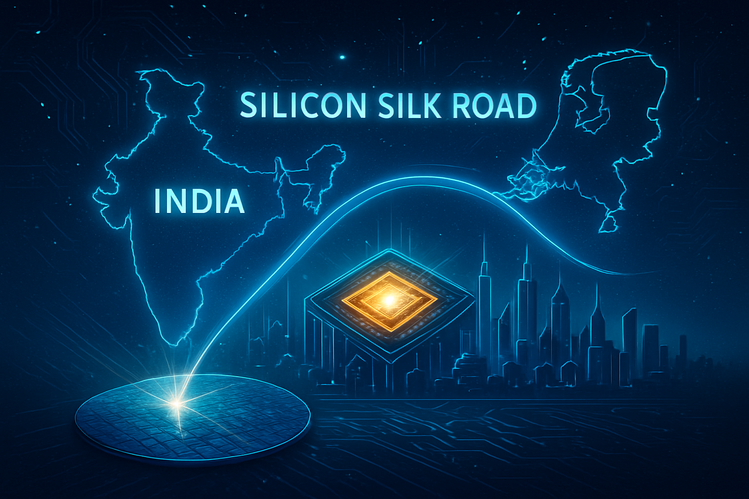
    As of January 26, 2026, the global semiconductor landscape has undergone a tectonic shift. What was once a policy-driven ambition for the Indian subcontinent has transformed into a tangible, high-output reality. At the center of this transformation is a pivotal partnership between Tata Electronics and ROHM Co., Ltd. (TYO: 6963), a Japanese pioneer in power and analog semiconductors. This alliance, focusing on the production of automotive-grade power MOSFETs (Metal-Oxide-Semiconductor Field-Effect Transistors), marks a critical milestone in India’s bid to offer a robust, democratic alternative to China’s long-standing dominance in mature-node manufacturing.

    The significance of this development extends far beyond simple hardware assembly. By localizing the production of high-current power management components, India is securing the physical backbone required for the next generation of AI-driven mobility and industrial automation. As the "China+1" strategy matures into a standard operating procedure for Western tech giants, the Tata-ROHM partnership stands as the first major proof of concept for India’s Semiconductor Mission (ISM) 2.0, successfully bridging the gap between design expertise and high-volume fabrication.

    Technical Prowess: Powering the Edge AI Revolution

    The technical centerpiece of the Tata-ROHM collaboration is the commercial rollout of an automotive-grade N-channel silicon MOSFET, specifically engineered for the rigorous demands of electric vehicles (EVs) and smart energy systems. Boasting a voltage rating of 100V and a current capacity of 300A, these chips utilize a TOLL (Transistor Outline Leadless) package. This modern surface-mount design is critical for high power density, offering superior thermal efficiency and lower parasitic inductance compared to traditional packaging. In the context of early 2026, where "Edge AI" in vehicles requires massive real-time processing, these power chips ensure that the high-current demands of onboard Neural Processing Units (NPUs) are met without compromising vehicle range or safety.

    This development is inextricably linked to the progress of India’s first mega-fab in Dholera, Gujarat—a $11 billion joint venture between Tata and Powerchip Semiconductor Manufacturing Corp (PSMC). As of this month, the Dholera facility has successfully completed high-volume trial runs using 300mm (12-inch) wafers. While the industry’s "bleeding edge" focuses on sub-5nm nodes, Tata’s strategic focus on the 28nm, 40nm, and 90nm "workhorse" nodes is a calculated move. These nodes are the essential foundations for Power Management ICs (PMICs), display drivers, and microcontrollers. Initial reactions from the industry have been overwhelmingly positive, with experts noting that India has bypassed the "learning curve" typically associated with greenfield fabs by integrating ROHM's established design IP directly into Tata’s manufacturing workflow.

    Market Impact: Navigating the 'China+1' Paradigm

    The market implications of this partnership are profound, particularly for the automotive and AI hardware sectors. Tata Motors (NSE: TATAMOTORS) and other global OEMs stand to benefit immensely from a shortened, more resilient supply chain that bypasses the geopolitical volatility associated with East Asian hubs. By establishing a reliable source of AEC-Q101 qualified semiconductors on Indian soil, the partnership offers a strategic hedge against potential sanctions or trade disruptions involving Chinese manufacturers like BYD (HKG: 1211).

    Furthermore, the involvement of Micron Technology (NASDAQ: MU)—whose Sanand facility reached full-scale commercial production in February 2026—and CG Power & Industrial Solutions (NSE: CGPOWER) creates a synergistic cluster. This ecosystem allows for "full-stack" manufacturing, where memory modules from Micron can be paired with power management chips from Tata-ROHM and logic chips from the Dholera fab. This vertical integration provides India with a unique competitive edge in the mid-range semiconductor market, which currently accounts for roughly 75% of global chip volume. Tech giants looking to diversify their hardware sourcing now view India not just as a consumer market, but as a critical export hub for the global AI and EV supply chains.

    The Geopolitical and AI Landscape: Beyond the Silicon

    The rise of the Tata-ROHM alliance must be viewed through the lens of the U.S.-India TRUST (Transforming the Relationship Utilizing Strategic Technology) initiative. This framework has paved the way for India to join the "Pax Silica" alliance, a group of nations committed to securing "trusted" silicon supply chains. For the global AI community, this means that the hardware required for "Sovereign AI"—data centers and AI-enabled infrastructure built within national borders—now has a secondary, reliable point of origin.

    In the data center space, the demand for Silicon Carbide (SiC) and Gallium Nitride (GaN) is exploding. These "Wide-Bandgap" materials are essential for the high-efficiency power units required by massive AI server racks featuring NVIDIA (NASDAQ: NVDA) Blackwell-architecture chips. The Tata-ROHM roadmap already signals a transition to SiC wafer production by 2027. By addressing the thermal and power density challenges of AI infrastructure, India is positioning itself as an indispensable partner in the global race for AI supremacy, ensuring that the energy-hungry demands of large language models (LLMs) are met by more efficient, locally-produced hardware.

    Future Horizons: From 28nm to the Bleeding Edge

    Looking ahead, the next 24 to 36 months will be decisive. Near-term expectations include the first commercial shipment of "Made in India" silicon from the Dholera fab by December 2026. However, the roadmap doesn't end at 28nm. Plans are already in motion for "Fab 2," which aims to target 14nm and eventually 7nm nodes to cater to the smartphone and high-performance computing (HPC) markets. The integration of advanced lithography systems from ASML (NASDAQ: ASML) into Indian facilities suggests that the technological ceiling is rapidly rising.

    The challenges remain significant: maintaining a consistent power supply, managing the high water-usage requirements of fabs, and scaling the specialized workforce. However, the Gujarat government's rapid infrastructure build-out—including thousands of residential units for semiconductor staff—demonstrates a level of political will rarely seen in industrial history. Analysts predict that by 2030, India could command a 10% share of the global semiconductor market, effectively neutralizing the risk of a single-point failure in the global electronics supply chain.

    A New Era for Global Manufacturing

    In summary, the partnership between Tata Electronics and ROHM is more than a corporate agreement; it is the cornerstone of a new global order in technology manufacturing. It signifies India's successful transition from a software-led economy to a hardware powerhouse capable of producing the most complex components of the modern age. The key takeaway for investors and industry leaders is clear: the semiconductor center of gravity is shifting.

    As we move deeper into 2026, the success of the Tata-ROHM venture will serve as a bellwether for India’s long-term semiconductor goals. The convergence of AI infrastructure needs, automotive electrification, and geopolitical realignments has created a "perfect storm" that India is now uniquely positioned to navigate. For the global tech industry, the emergence of this Indian silicon shield provides a much-needed layer of resilience in an increasingly uncertain world.


    This content is intended for informational purposes only and represents analysis of current AI developments.

    TokenRing AI delivers enterprise-grade solutions for multi-agent AI workflow orchestration, AI-powered development tools, and seamless remote collaboration platforms.
    For more information, visit https://www.tokenring.ai/.

  • India Outlines “Product-Led” Roadmap for Semiconductor Leadership at VLSI 2026

    India Outlines “Product-Led” Roadmap for Semiconductor Leadership at VLSI 2026

    At the 39th International VLSI Design & Embedded Systems Conference (VLSID 2026) held in Pune this month, India officially shifted its semiconductor strategy from a focus on assembly to a high-stakes "product-led" roadmap. Industry leaders and government officials unveiled a vision to transform the nation into a global semiconductor powerhouse by 2030, moving beyond its traditional role as a back-office design hub to becoming a primary architect of indigenous silicon. This development marks a pivotal moment in the global tech landscape, as India aggressively positions itself to capture the burgeoning demand for chips in the automotive, telecommunications, and AI sectors.

    The announcement comes on the heels of major construction milestones at the Tata Electronics mega-fab in Dholera, Gujarat. With "First Silicon" production now slated for December 2026, the Indian government is doubling down on a workforce strategy that leverages cutting-edge "virtual twin" simulations. This digital-first approach aims to train a staggering one million chip-ready engineers by 2030, a move designed to solve the global talent shortage while providing a resilient, democratic alternative to China’s dominance in mature semiconductor nodes.

    Technical Foundations: Virtual Twins and the Path to 28nm

    The technical centerpiece of the VLSI 2026 roadmap is the integration of "Virtual Twin" technology into India’s educational and manufacturing sectors. Spearheaded by a partnership with Lam Research (NASDAQ: LRCX), the initiative utilizes the SEMulator3D platform to create high-fidelity, virtual nanofabrication environments. These digital sandboxes allow engineering students to simulate complex manufacturing processes—including deposition, etching, and lithography—without the prohibitive cost of physical cleanrooms. This enables India to scale its workforce rapidly, training approximately 60,000 engineers annually in a "virtual fab" before they ever step onto a physical production floor.

    On the manufacturing side, the Tata Electronics facility, a joint venture with Taiwan’s Powerchip Semiconductor Manufacturing Corporation (PSMC), is targeting the 28nm node as its initial production benchmark. While the 28nm process is often considered a "mature" node, it remains the industry's "sweet spot" for automotive power management, 5G infrastructure, and IoT devices. The Dholera fab is designed for a capacity of 50,000 wafers per month, utilizing advanced immersion lithography to balance cost-efficiency with high performance. This provides a robust foundation for the India Semiconductor Mission’s (ISM) next phase: a leap toward 7nm and 3nm design centers already being established in Noida and Bengaluru.

    This "product-led" approach differs significantly from previous iterations of the ISM, which focused heavily on attracting Outsourced Semiconductor Assembly and Test (OSAT) facilities. By prioritizing domestic Intellectual Property (IP) and end-to-end design for the automotive and telecom sectors, India is moving up the value chain. Initial reactions from the AI research community have been overwhelmingly positive, with experts noting that India’s focus on the 28nm–90nm segments could mitigate future supply chain shocks for the global EV market, which has historically been over-reliant on a handful of East Asian suppliers.

    Market Dynamics: A "China+1" Reality

    The strategic pivot outlined at VLSI 2026 has immediate implications for global tech giants and the competitive balance of the semiconductor industry. Major players like Intel (NASDAQ: INTC), AMD (NASDAQ: AMD), and NVIDIA (NASDAQ: NVDA) were present at the conference, signaling a growing consensus that India is no longer just a source of talent but a critical market and manufacturing partner. Companies like Qualcomm (NASDAQ: QCOM) stand to benefit immensely from India’s focus on indigenous telecom chips, potentially reducing their manufacturing costs while gaining preferential access to the world’s fastest-growing mobile market.

    For the Tata Group, particularly Tata Motors (NYSE: TTM), the roadmap provides a path toward vertical integration. By designing and manufacturing its own automotive chips, Tata can insulate its vehicle production from the volatility of the global chip market. Furthermore, software-industrial giants like Siemens (OTCMKTS: SIEGY) and Dassault Systèmes (OTCMKTS: DASTY) are finding a massive new market for their Electronic Design Automation (EDA) and digital twin software, as the Indian government mandates their use across specialized VLSI curriculum tracks in hundreds of universities.

    The competitive implications for China are stark. India is positioning itself as the primary "China+1" alternative, emphasizing its democratic regulatory environment and transparent IP protections. By targeting the $110 billion domestic demand for semiconductors by 2030, India aims to undercut China’s market share in mature nodes while simultaneously building the infrastructure for advanced AI silicon. This strategy forces a realignment of global supply chains, as western companies seek to diversify their manufacturing footprints away from geopolitical flashpoints.

    The Broader AI and Societal Landscape

    The "product-led" roadmap is inextricably linked to the broader AI revolution. As AI moves from massive data centers to "edge" devices—such as autonomous vehicles and smart city infrastructure—the need for specialized, energy-efficient silicon becomes paramount. India’s focus on designing chips for these specific use cases places it at the heart of the "Edge AI" trend. This development mirrors previous milestones like the rise of the Taiwan semiconductor ecosystem in the 1990s, but at a significantly accelerated pace driven by modern simulation tools and AI-assisted chip design.

    However, the ambitious plan is not without concerns. Scaling a workforce to one million engineers requires a radical overhaul of the national education system, a feat that has historically faced bureaucratic hurdles. Critics also point to the immense water and power requirements of semiconductor fabs, raising questions about the sustainability of the Dholera project in a water-stressed region. Comparisons to the early days of China's "Big Fund" suggest that while capital is essential, the long-term success of the ISM will depend on India's ability to maintain political stability and consistent policy support over the next decade.

    Despite these challenges, the societal impact of this roadmap is profound. The creation of a high-tech manufacturing base offers a path toward massive job creation and middle-class expansion. By shifting from a service-based economy to a high-value manufacturing and design hub, India is attempting to replicate the economic transformations seen in South Korea and Taiwan, but on a scale never before attempted in the democratic world.

    Looking Ahead: The Roadmap to 2030

    In the near term, the industry will be watching for the successful installation of equipment at the Dholera fab throughout 2026. The next eighteen months are critical; any delays in "First Silicon" could dampen investor confidence. However, the projected applications for these chips—ranging from 5G base stations to indigenous AI accelerators for agriculture and healthcare—offer a glimpse into a future where India is a net exporter of high-technology products.

    Experts predict that by 2028, we will see the first generation of "Designed in India, Made in India" processors hitting the global market. The challenge will be moving from the "bread and butter" 28nm nodes to the sub-10nm frontier required for high-end AI training. If the current trajectory holds, the 1.60 lakh crore rupee investment will serve as the seed for a trillion-dollar domestic electronics industry, fundamentally altering the global technological hierarchy.

    Summary and Final Thoughts

    The VLSI 2026 conference has solidified India’s position as a serious contender in the global semiconductor race. The shift toward a product-led strategy, backed by the construction of the Tata Electronics fab and a revolutionary "virtual twin" training model, marks the beginning of a new chapter in Indian industrial history. Key takeaways include the nation's focus on mature nodes for the "Edge AI" and automotive markets, and its aggressive pursuit of a one-million-strong workforce to solve the global talent gap.

    As we look toward the end of 2026, the success of the Dholera fab will be the ultimate litmus test for the India Semiconductor Mission. In the coming months, the tech world should watch for further partnerships between the Indian government and global EDA providers, as well as the progress of the 24 chip design startups currently vying to become India’s first semiconductor unicorns. The silicon wars have a new front, and India is no longer just a spectator—it is an architect.


    This content is intended for informational purposes only and represents analysis of current AI developments.

    TokenRing AI delivers enterprise-grade solutions for multi-agent AI workflow orchestration, AI-powered development tools, and seamless remote collaboration platforms.
    For more information, visit https://www.tokenring.ai/.

  • India’s Semiconductor Rise: The Rohm and Tata Partnership

    India’s Semiconductor Rise: The Rohm and Tata Partnership

    In a landmark move that cements India’s position as a burgeoning titan in the global technology supply chain, Rohm Co., Ltd. (TYO: 6963) and Tata Electronics have officially entered into a strategic partnership to establish a domestic semiconductor manufacturing ecosystem. Announced on December 22, 2025, this collaboration focuses on the high-growth sector of power semiconductors—the essential hardware that manages electricity in everything from electric vehicle (EV) drivetrains to the massive data centers powering modern artificial intelligence.

    The partnership represents a critical milestone for the India Semiconductor Mission (ISM), a $10 billion government initiative designed to reduce reliance on foreign imports and build a "China Plus One" alternative for global electronics. By combining Rohm’s decades of expertise in Integrated Device Manufacturing (IDM) with the industrial scale of the Tata Group, the two companies aim to localize the entire value chain—from design and wafer fabrication to advanced packaging and testing—positioning India as a primary node in the global chip architecture.

    Powering the Future: Technical Specifications and the Shift to Wide-Bandgap Materials

    The technical core of the Rohm-Tata partnership centers on the production of advanced power semiconductors, which are significantly more complex to manufacture than standard logic chips. The first product slated for production is an India-designed, automotive-grade N-channel 100V, 300A Silicon MOSFET. This device utilizes a TOLL (Transistor Outline Leadless) package, a specialized form factor that offers superior thermal management and high current density, making it ideal for the demanding power-switching requirements of modern electric drivetrains and industrial automation.

    Beyond traditional silicon, the collaboration is heavily focused on "wide-bandgap" (WBG) materials, specifically Silicon Carbide (SiC) and Gallium Nitride (GaN). Rohm is a recognized global leader in SiC technology, which allows for higher voltage operation and significantly faster switching speeds than traditional silicon. In practical terms, SiC modules can reduce switching losses by up to 85%, a technical leap that is essential for extending the range of EVs and shrinking the footprint of the power inverters used in AI-driven smart grids.

    This approach differs from previous attempts at Indian semiconductor manufacturing by focusing on "specialty" chips rather than just chasing the smallest nanometer nodes. While the industry often focuses on 3nm or 5nm logic chips for CPUs, the power semiconductors being developed by Rohm and Tata are the "muscles" of the digital world. Industry experts note that by securing the supply of these specialized components, India is addressing a critical bottleneck in the global supply chain that was exposed during the shortages of 2021-2022.

    Market Disruption: Tata’s Manufacturing Might Meets Rohm’s Design Prowess

    The strategic implications of this deal for the global market are profound. Tata Electronics, a subsidiary of the storied Tata Group, is leveraging its massive new facilities in Jagiroad, Assam, and Dholera, Gujarat, to provide the backend infrastructure. The Jagiroad Assembly and Test (ATMP) facility, a $3.2 billion investment, has already begun commissioning and is expected to handle the bulk of the Rohm-designed chip packaging. This allows Rohm to scale its production capacity without the massive capital expenditure of building new wholly-owned fabs in Japan or Malaysia.

    For the broader tech ecosystem, the partnership creates a formidable competitor to established players in the power semi space like Infineon and STMicroelectronics. Companies within the Tata umbrella, such as Tata Motors (NSE: TATAMOTORS) and Tata Elxsi (NSE: TATAELXSI), stand to benefit immediately from a localized, secure supply of high-efficiency chips. This vertical integration provides a significant strategic advantage, insulating the Indian automotive and aerospace sectors from geopolitical volatility in the Taiwan Strait or the South China Sea.

    Furthermore, the "Designed in India, Manufactured in India" nature of this partnership qualifies it for the highest tier of government incentives. Under the ISM, the project receives nearly 50% fiscal support for capital expenditure, a level of subsidy that makes the Indian-produced chips highly competitive on the global export market. This cost advantage, combined with Rohm’s reputation for reliability, is expected to attract major global OEMs looking to diversify their supply chains away from East Asian hubs.

    The Geopolitical Shift: India as a Global Semiconductor Hub

    The Rohm-Tata partnership is more than just a corporate deal; it is a manifestation of the "China Plus One" strategy that is reshaping global geopolitics. As the United States and its allies continue to restrict the flow of advanced AI hardware to certain regions, India is positioning itself as a neutral, democratic alternative for high-tech manufacturing. This development fits into a broader trend where India is no longer just a consumer of technology but a critical architect of the hardware that runs it.

    This shift has massive implications for the AI landscape. While much of the public discourse around AI focuses on Large Language Models (LLMs), the physical infrastructure—the data centers and cooling systems—requires sophisticated power management. The SiC and GaN chips produced by this partnership are the very components that make "Green AI" possible by reducing the energy footprint of massive server farms. By localizing this production, India is ensuring that its own AI ambitions are supported by a resilient and efficient hardware foundation.

    The significance of this milestone can be compared to the early days of the IT services boom in India, but with a much higher barrier to entry. Unlike software, semiconductor manufacturing requires extreme precision, stable power, and a highly specialized workforce. The success of the Rohm-Tata venture will serve as a "proof of concept" for other global giants like Intel (NASDAQ: INTC) or TSMC (NYSE: TSM), who are closely watching India’s ability to execute on these complex manufacturing projects.

    The Road Ahead: Fabs, Talent, and the 2026 Horizon

    Looking toward the near future, the next major milestone will be the completion of the Dholera Fab in Gujarat. While initial production is focused on assembly and testing (the "backend"), the Dholera facility is designed for front-end wafer fabrication. Trials are expected to begin in early 2026, with the first commercial wafers in the 28nm to 110nm range slated for late 2026. This will complete the "sand-to-chip" cycle within Indian borders, a feat achieved by only a handful of nations.

    However, challenges remain. The industry faces a significant talent gap, requiring thousands of specialized engineers to operate these facilities. To address this, Tata and Rohm are expected to launch joint training programs and university partnerships across India. Additionally, the infrastructure in Dholera and Jagiroad—including ultra-pure water supplies and uninterrupted green energy—must be maintained at world-class standards to ensure the high yields necessary for semiconductor profitability.

    Experts predict that if the Rohm-Tata partnership meets its 2026 targets, India could become a net exporter of power semiconductors by 2028. This would not only balance India’s trade deficit in electronics but also provide the country with significant "silicon diplomacy" leverage on the world stage, as global industries become increasingly dependent on Indian-made SiC and GaN modules.

    Conclusion: A New Chapter in the Silicon Century

    The partnership between Rohm and Tata Electronics marks a definitive turning point in India’s industrial history. By focusing on the high-efficiency power semiconductors that are essential for the AI and EV eras, the collaboration bypasses the "commodity chip" trap and moves straight into high-value, high-complexity manufacturing. The support of the India Semiconductor Mission has provided the necessary financial tailwinds, but the real test will be the operational execution over the next 18 months.

    As we move into 2026, the tech world will be watching the Jagiroad and Dholera facilities closely. The success of these sites will determine if India can truly sustain a semiconductor ecosystem that rivals the established hubs of East Asia. For now, the Rohm-Tata alliance stands as a bold statement of intent: the future of the global chip supply chain is no longer just about where the chips are designed, but where the power to run the future is built.


    This content is intended for informational purposes only and represents analysis of current AI and semiconductor developments.

    TokenRing AI delivers enterprise-grade solutions for multi-agent AI workflow orchestration, AI-powered development tools, and seamless remote collaboration platforms.
    For more information, visit https://www.tokenring.ai/.

  • Silicon Sovereignty: Tata and ROHM Forge Strategic Alliance to Power India’s Semiconductor Revolution

    Silicon Sovereignty: Tata and ROHM Forge Strategic Alliance to Power India’s Semiconductor Revolution

    In a landmark development for the global electronics supply chain, Tata Electronics has officially entered into a strategic partnership with Japan’s ROHM Co., Ltd. (TYO: 6963) to manufacture power semiconductors in India. Announced today, December 22, 2025, this collaboration marks a pivotal moment in India’s ambitious journey to transition from a software-centric economy to a global hardware and semiconductor manufacturing powerhouse. The deal focuses on the joint development and production of high-efficiency power devices, specifically targeting the burgeoning electric vehicle (EV) and industrial automation sectors.

    This partnership is not merely a bilateral agreement; it is the cornerstone of India’s broader strategy to secure its technological sovereignty. By integrating ROHM’s world-class expertise in wide-bandgap semiconductors with the massive industrial scale of the Tata Group, India is positioning itself to capture a significant share of the $80 billion global power semiconductor market. The move is expected to drastically reduce the nation’s reliance on imported silicon components, providing a stable, domestic supply chain for Indian automotive giants like Tata Motors (NSE: TATAMOTORS) and green energy leaders like Tata Power (NSE: TATAPOWER).

    Technical Breakthroughs: Silicon Carbide and the Future of Power Efficiency

    The technical core of the Tata-ROHM alliance centers on the manufacturing of advanced power discrete components. Initially, the partnership will focus on the assembly and testing of automotive-grade Silicon (Si) MOSFETs—specifically the Nch 100V, 300A variants—designed for high-current applications in electric drivetrains. However, the true disruptive potential lies in the roadmap for "Wide-Bandgap" (WBG) materials, including Silicon Carbide (SiC) and Gallium Nitride (GaN). Unlike traditional silicon, SiC and GaN allow for higher voltage operation, faster switching speeds, and significantly better thermal management, which are essential for extending the range and reducing the charging times of modern EVs.

    This collaboration differs from previous semiconductor initiatives in India by focusing on the "power" segment rather than just logic chips. Power semiconductors are the "muscles" of electronic systems, managing how electricity is converted and distributed. By establishing a dedicated production line for these components at Tata’s new Outsourced Semiconductor Assembly and Test (OSAT) facility in Jagiroad, Assam, the partnership ensures that India can produce chips that are up to 50% more efficient than current standards. Industry experts have lauded the move, noting that ROHM’s proprietary SiC technology is among the most advanced in the world, and its transfer to Indian soil represents a major leap in domestic technical capability.

    Market Disruption: Shifting the Global Semiconductor Balance of Power

    The strategic implications for the global tech landscape are profound. For years, the semiconductor industry has been heavily concentrated in East Asia, leaving global markets vulnerable to geopolitical tensions and supply chain bottlenecks. The Tata-ROHM partnership, backed by the Indian government’s $10 billion India Semiconductor Mission (ISM), provides a viable "China Plus One" alternative for global OEMs. Major tech giants and automotive manufacturers seeking to diversify their sourcing will now look toward India as a high-tech manufacturing hub that offers both scale and competitive cost structures.

    Within India, the primary beneficiaries will be the domestic EV ecosystem. Tata Motors (NSE: TATAMOTORS), which currently dominates the Indian electric car market, will gain a first-mover advantage by integrating locally-produced, high-efficiency chips into its future vehicle platforms. Furthermore, the partnership poses a competitive challenge to established European and American power semiconductor firms. By leveraging India’s lower operational costs and ROHM’s engineering prowess, the Tata-ROHM venture could potentially disrupt the pricing models for power modules globally, forcing competitors to accelerate their own investments in emerging markets.

    A National Milestone: India’s Transition to a Global Chip Hub

    This announcement fits into a broader trend of "techno-nationalism," where nations are racing to build domestic chip capabilities to ensure economic and national security. The Tata-ROHM deal is the latest in a series of high-profile successes for the India Semiconductor Mission. It follows the massive ₹91,000 crore investment in the Dholera mega-fab, a joint venture between Tata Electronics and Powerchip Semiconductor Manufacturing Corp (TPE: 6770), and the entry of Micron Technology (NASDAQ: MU) into the Indian packaging space. Together, these projects signal that India has moved past the "planning" phase and is now in the "execution" phase of its semiconductor roadmap.

    However, the rapid expansion is not without its challenges. The industry remains concerned about the availability of specialized ultra-pure water and uninterrupted high-voltage power—critical requirements for semiconductor fabrication. Comparisons are already being made to the early days of China’s semiconductor rise, with analysts noting that India’s democratic framework and strong intellectual property protections may offer a more stable long-term environment for international partners. The success of the Tata-ROHM partnership will serve as a litmus test for whether India can successfully manage the complex logistics of high-tech manufacturing at scale.

    The Road Ahead: 2026 and the Leap Toward "Semicon 2.0"

    Looking toward 2026, the partnership is expected to move into full-scale mass production. The Jagiroad facility in Assam is projected to reach a daily output of 48 million chips by early next year, while the Dholera fab will begin pilot runs for 28nm logic chips. The next frontier for the Tata-ROHM collaboration will be the integration of Artificial Intelligence (AI) into the manufacturing process. AI-driven predictive maintenance and yield optimization are expected to be implemented at the Dholera plant, making it one of the most advanced "Smart Fabs" in the world.

    Beyond manufacturing, the Indian government is already preparing for "Semicon 2.0," a second phase of incentives that will likely double the current financial outlay to $20 billion. This phase will focus on the upstream supply chain, including specialized chemicals, gases, and wafer production. Experts predict that if the current momentum continues, India could account for nearly 10% of the global semiconductor assembly and testing market by 2030, fundamentally altering the geography of the digital age.

    Conclusion: A New Era for Indian Electronics

    The partnership between Tata Electronics and ROHM Co., Ltd. is more than a business deal; it is a declaration of intent. It signifies that India is no longer content with being the world’s back-office for software but is ready to build the physical foundations of the future. By securing a foothold in the critical power semiconductor market, India is ensuring that its transition to a green, electrified economy is built on a foundation of domestic innovation and manufacturing.

    As we move into 2026, the world will be watching the progress of the Jagiroad and Dholera facilities with intense interest. The success of these projects will determine whether India can truly become the "third pillar" of the global semiconductor industry, alongside East Asia and the West. For now, the Tata-ROHM alliance stands as a testament to the power of international collaboration in solving the world's most complex technological challenges.


    This content is intended for informational purposes only and represents analysis of current AI and semiconductor developments as of December 22, 2025.

    TokenRing AI delivers enterprise-grade solutions for multi-agent AI workflow orchestration, AI-powered development tools, and seamless remote collaboration platforms.
    For more information, visit https://www.tokenring.ai/.

  • The Silicon Silk Road: India and the Netherlands Forge a New Semiconductor Axis for the AI Era

    The Silicon Silk Road: India and the Netherlands Forge a New Semiconductor Axis for the AI Era

    In a move that signals a tectonic shift in the global technology landscape, India and the Netherlands have today, December 19, 2025, finalized the "Silicon Silk Road" strategic alliance. This comprehensive framework, signed in New Delhi, aims to bridge the gap between European high-tech precision and Indian industrial scale. By integrating the Netherlands’ world-leading expertise in lithography and semiconductor equipment with India’s rapidly expanding manufacturing ecosystem, the partnership seeks to create a resilient, alternative supply chain for the high-performance hardware required to power the next generation of artificial intelligence.

    The immediate significance of this alliance cannot be overstated. As the global demand for AI-optimized chips—specifically those capable of handling massive large language model (LLM) training and edge computing—reaches a fever pitch, the "Silicon Silk Road" provides a blueprint for a decentralized manufacturing future. The agreement moves beyond simple trade, establishing a co-development model that includes technology transfers, joint R&D in advanced materials, and the creation of specialized maintenance hubs that will ensure India’s upcoming fabrication units (fabs) operate with the world’s most advanced Dutch-made machinery.

    Technical Foundations: Lithography, Labs, and Lab-Grown Diamonds

    The core of the alliance is built upon unprecedented commitments from Dutch semiconductor giants. NXP Semiconductors N.V. (NASDAQ:NXPI) has officially announced a massive $1 billion investment to double its research and development presence in India. This expansion is focused on the design of 5-nanometer automotive and AI chips, with a new R&D center slated for the Greater Noida Semiconductor Park. Unlike previous design-only centers, this facility will work in tandem with Indian manufacturing partners to prototype "system-on-chip" (SoC) architectures specifically optimized for low-latency AI applications.

    Simultaneously, ASML Holding N.V. (NASDAQ:ASML) is shifting its strategy from a vendor-client relationship to a deep-tier partnership. For the first time, ASML will establish "Holistic Lithography" maintenance labs within India. These labs are designed to provide real-time technical support and software calibration for the Extreme Ultraviolet (EUV) and Deep Ultraviolet (DUV) lithography systems that are essential for high-end chip production. This differs from existing models where technical expertise was centralized in Europe or East Asia, effectively removing a significant bottleneck for Indian fab operators like the Tata Group and Micron Technology, Inc. (NASDAQ:MU).

    One of the most technically ambitious aspects of the 2025 framework is the joint research into lab-grown diamonds (LGD) as a substrate for semiconductors. Leveraging India’s established diamond-processing hub in Surat and Dutch precision engineering, the partnership aims to develop diamond-based chips that can handle significantly higher thermal loads than traditional silicon. This breakthrough could revolutionize AI hardware, where heat management is currently a primary limiting factor for processing density in data centers.

    Strategic Realignment: Winners in the New Hardware Race

    The "Silicon Silk Road" creates a new competitive theater for the world’s largest AI labs and hardware providers. Companies like NVIDIA Corporation (NASDAQ:NVDA) and Advanced Micro Devices, Inc. (NASDAQ:AMD) stand to benefit immensely from a more diversified manufacturing base. By having a viable, Dutch-supported manufacturing alternative in India, these tech giants can mitigate the geopolitical risks associated with the current concentration of production in East Asia. The alliance provides a "China+1" strategy with teeth, offering a stable environment backed by European intellectual property protections and Indian production-linked incentives (PLI).

    For the Netherlands, the alliance secures a massive, long-term market for its high-tech exports at a time when global trade restrictions are tightening. ASML and NXP are effectively "future-proofing" their revenue streams by embedding themselves into the foundation of India’s digital infrastructure. Meanwhile, Indian tech conglomerates and startups are gaining access to the "holy grail" of semiconductor manufacturing: the ability to move from chip design to domestic fabrication with the support of the world’s most advanced equipment manufacturers. This positioning gives Indian firms a strategic advantage in the burgeoning field of "Sovereign AI," where nations seek to control their own computational resources.

    Geopolitics and the Global AI Landscape

    The emergence of the Silicon Silk Road fits into a broader trend of "techno-nationalism," where semiconductor self-sufficiency is viewed as a pillar of national security. This partnership is a direct response to the fragility of global supply chains exposed during the early 2020s. By forging this link, India and the Netherlands are creating a middle path that avoids the binary choice between US-led and China-led ecosystems. It is a milestone comparable to the early 2000s outsourcing boom, but with a critical difference: this time, India is moving up the value chain into the most complex manufacturing process ever devised by humanity.

    However, the alliance does not come without concerns. Industry analysts have pointed to the immense energy requirements of advanced fabs and the potential environmental impact of large-scale semiconductor manufacturing in India. Furthermore, the transfer of highly sensitive lithography technology requires a level of cybersecurity and intellectual property protection that will be a constant test for Indian regulators. Comparing this to previous milestones like the CHIPS Act, the Silicon Silk Road is unique because it relies on bilateral synergy rather than unilateral subsidies, blending Dutch technical precision with India’s demographic dividend.

    The Horizon: 2026 and Beyond

    Looking ahead, the next 24 months will be critical for the execution of the 2025 framework. The immediate goal is the operationalization of the first joint R&D labs and the commencement of training for the first cohort of 85,000 semiconductor professionals that India aims to produce by 2030. Near-term developments will likely include the announcement of a joint venture between an Indian industrial house and a Dutch equipment firm to manufacture semiconductor components—not just chips—locally, further deepening the supply chain.

    The long-term vision involves the commercialization of the lab-grown diamond substrate technology, which could place the India-Netherlands axis at the forefront of "Beyond Silicon" computing. Experts predict that by 2028, the first AI accelerators featuring "Made in India" chips, fabricated using ASML-supported systems, will hit the global market. The primary challenge will be maintaining the pace of infrastructure development—specifically stable power and ultra-pure water supplies—to match the requirements of the high-tech machinery being deployed.

    Conclusion: A New Chapter in Industrial History

    The signing of the Silicon Silk Road alliance marks the end of an era where semiconductor manufacturing was the exclusive domain of a few select geographies. It represents a maturation of India’s industrial ambitions and a strategic pivot for the Netherlands as it seeks to maintain its technological edge in an increasingly fragmented world. The key takeaway is clear: the future of AI hardware will not be determined by a single nation, but by the strength and resilience of the networks they build.

    As we move into 2026, the global tech community will be watching the progress in Greater Noida and the research labs of Eindhoven with intense interest. The success of this partnership could serve as a model for other nations looking to secure their technological future. For now, the "Silicon Silk Road" stands as a testament to the power of strategic collaboration in the age of artificial intelligence, promising to reshape the hardware that will define the rest of the 21st century.


    This content is intended for informational purposes only and represents analysis of current AI developments.

    TokenRing AI delivers enterprise-grade solutions for multi-agent AI workflow orchestration, AI-powered development tools, and seamless remote collaboration platforms.
    For more information, visit https://www.tokenring.ai/.

  • The Great Silicon Migration: Global Semiconductor Maps Redrawn as US and India Hit Key Milestones

    The Great Silicon Migration: Global Semiconductor Maps Redrawn as US and India Hit Key Milestones

    The global semiconductor landscape has reached a historic turning point. As of late 2025, the multi-year effort to diversify the world’s chip supply chain away from its heavy concentration in Taiwan has transitioned from a series of legislative promises into a tangible, operational reality. With the United States successfully bringing its first advanced "onshored" logic fabs online and India emerging as a critical hub for back-end assembly, the geographical monopoly on high-end silicon is finally beginning to fracture. This shift represents the most significant restructuring of the technology industry’s physical foundation in over four decades, driven by a combination of geopolitical de-risking and the insatiable hardware demands of the generative AI era.

    The immediate significance of this migration cannot be overstated for the AI industry. For years, the concentration of advanced node production in a single geographic region—Taiwan—posed a systemic risk to global stability and the AI revolution. Today, the successful volume production of 4nm chips at Taiwan Semiconductor Manufacturing Co. (NYSE: TSM)'s Arizona facility and the commencement of 1.8nm-class production by Intel Corporation (NASDAQ: INTC) mark the birth of a "Silicon Heartland" in the West. These developments provide a vital safety valve for AI giants like NVIDIA (NASDAQ: NVDA) and Advanced Micro Devices (NASDAQ: AMD), ensuring that the next generation of AI accelerators will have a diversified manufacturing base.

    Advanced Logic Moves West: The Technical Frontier

    The technical achievements of 2025 have silenced many skeptics who doubted the feasibility of migrating ultra-advanced manufacturing processes to U.S. soil. TSMC’s Fab 21 in Arizona is now in full volume production of 4nm (N4P) chips, achieving yields that are reportedly identical to those in its Hsinchu headquarters. This facility is currently supplying the high-performance silicon required for the latest mobile processors and AI edge devices. Meanwhile, Intel has reached a critical milestone with its 18A (1.8nm) node in Oregon and Arizona. By utilizing revolutionary RibbonFET gate-all-around (GAA) transistors and PowerVia backside power delivery, Intel has managed to leapfrog traditional scaling limits, positioning its foundry services as a direct competitor to TSMC for the most demanding AI workloads.

    In contrast to the U.S. focus on leading-edge logic, the diversification effort in Europe and India has taken a more specialized technical path. In Europe, the European Chips Act has fostered a stronghold in "foundational" nodes. The ESMC project in Dresden—a joint venture between TSMC, Infineon Technologies (OTCMKTS: IFNNY), NXP Semiconductors (NASDAQ: NXPI), and Robert Bosch GmbH—is currently installing equipment for 28nm and 16nm FinFET production. These nodes are technically optimized for the high-reliability requirements of the automotive and industrial sectors, ensuring that the European AI-driven automotive industry is not paralyzed by future supply shocks.

    India has carved out a unique position by focusing on the "back-end" of the supply chain and foundational logic. The Tata Group's first commercial-scale fab in Dholera, Gujarat, is currently under construction with a focus on 28nm nodes, which are essential for power management and communication chips. More importantly, Micron Technology (NASDAQ: MU) has successfully operationalized its $2.7 billion assembly, testing, marking, and packaging (ATMP) facility in Sanand, Gujarat. This facility is the first of its kind in India, handling the complex final stages of memory production that are critical for High Bandwidth Memory (HBM) used in AI data centers.

    Strategic Advantages for the AI Ecosystem

    This geographic redistribution of manufacturing capacity creates a new competitive dynamic for AI companies and tech giants. For companies like Apple (NASDAQ: AAPL) and Nvidia, the ability to source chips from multiple jurisdictions provides a powerful strategic hedge. It reduces the "single-source" risk that has long been a vulnerability in their SEC filings. By having access to TSMC’s Arizona fabs and Intel’s 18A capacity, these companies can better negotiate pricing and ensure a steady supply of silicon even in the event of regional instability in East Asia.

    The competitive implications are particularly stark for the foundry market. Intel’s successful rollout of its 18A node has transformed it into a credible "Western Foundry" alternative, attracting interest from AI startups and established labs that prioritize domestic security and IP protection. Conversely, Samsung Electronics (OTCMKTS: SSNLF) has made a strategic pivot at its Taylor, Texas facility, delaying 4nm production to move directly to 2nm (SF2) nodes by 2026. This "leapfrog" strategy is designed to capture the next wave of AI accelerator contracts, as the industry moves beyond current-generation architectures toward more energy-efficient 2nm designs.

    Geopolitics and the New Silicon Map

    The wider significance of these developments lies in the decoupling of the technology supply chain from geopolitical flashpoints. For decades, the "Silicon Shield" of Taiwan was seen as a deterrent to conflict, but the AI boom has made chip supply a matter of national security. The diversification into the U.S., Europe, and India represents a shift toward "friend-shoring," where manufacturing is concentrated in allied nations. This trend, however, has not been without its setbacks. The mid-2025 cancellation of Intel’s planned mega-fabs in Germany and Poland served as a sobering reminder that economic reality and corporate restructuring can still derail even the most ambitious government-backed plans.

    Despite these hurdles, the broader trend is clear: the era of extreme concentration is ending. This fits into a larger pattern of "resilience over efficiency" that has characterized the post-pandemic global economy. While building chips in Arizona or Dresden is undeniably more expensive than in Taiwan or South Korea, the industry has collectively decided that the cost of a total supply chain collapse is infinitely higher. This mirrors previous shifts in other critical industries, such as energy and aerospace, where geographic redundancy is considered a baseline requirement for survival.

    The Road Ahead: 1.4nm and Beyond

    Looking toward 2026 and 2027, the focus will shift from building "shells" to installing the next generation of lithography equipment. The deployment of ASML (NASDAQ: ASML)'s High-NA EUV (Extreme Ultraviolet) scanners will be the next major battleground. Intel’s Ohio "Silicon Heartland" site, though facing structural delays, is being prepared as a primary hub for 14A (1.4nm) production using these advanced tools. Experts predict that the next three years will see a "capacity war" as regions compete to prove they can not only build the chips but also sustain the complex ecosystem of chemicals, gases, and specialized labor required to keep the fabs running.

    One of the most significant challenges remaining is the talent gap. Both the U.S. and India are racing to train tens of thousands of specialized engineers required to operate these facilities. The success of the India Semiconductor Mission (ISM) will depend heavily on its ability to transition from assembly and testing into high-end wafer fabrication. If India can successfully bring the Tata-PSMC fab online by 2027, it will cement its place as the third major pillar of the global semiconductor supply chain, alongside East Asia and the West.

    A New Era of Hardware Sovereignty

    The events of 2025 mark the end of the first chapter of the "Great Silicon Migration." The key takeaway is that the global semiconductor map has been successfully redrawn. While Taiwan remains the undisputed leader in volume and advanced node expertise, it is no longer the world’s only option. The operational status of TSMC Arizona and the emergence of India’s assembly ecosystem have created a more resilient, albeit more expensive, foundation for the future of artificial intelligence.

    In the coming months, industry watchers should keep a close eye on the yield rates of Samsung’s 2nm pivot in Texas and the progress of the ESMC project in Germany. These will be the litmus tests for whether the diversification effort can maintain its momentum without the massive government subsidies that characterized its early years. For now, the AI industry can breathe a sigh of relief: the physical infrastructure of the digital age is finally starting to look as global as the code that runs upon it.


    This content is intended for informational purposes only and represents analysis of current AI developments.

    TokenRing AI delivers enterprise-grade solutions for multi-agent AI workflow orchestration, AI-powered development tools, and seamless remote collaboration platforms.
    For more information, visit https://www.tokenring.ai/.

  • The Silicon Desert Rises: India’s Gujarat Emerges as the World’s Newest Semiconductor Powerhouse

    The Silicon Desert Rises: India’s Gujarat Emerges as the World’s Newest Semiconductor Powerhouse

    As of December 18, 2025, the global technology landscape is witnessing a seismic shift as India’s "Silicon Desert" in Gujarat transitions from a vision of self-reliance to a tangible manufacturing reality. Just months after CG Power and Industrial Solutions Ltd (NSE: CGPOWER) produced the first "Made in India" semiconductor chip from its Sanand pilot line, the state has become the epicenter of a multi-billion dollar industrial explosion. This expansion, fueled by the India Semiconductor Mission (ISM) and a unique integration of massive renewable energy projects, marks India's official entry into the high-stakes global chip supply chain, positioning the nation as a viable alternative to traditional hubs in East Asia.

    The momentum in Gujarat is anchored by three massive projects that have moved from blueprints to high-gear execution throughout 2025. In Dholera, the Tata Electronics and Powerchip Semiconductor Manufacturing Corp (PSMC) joint venture is currently in a massive construction phase for India’s first commercial mega-fab. Meanwhile, Micron Technology (NASDAQ: MU) is nearing the completion of its $2.75 billion Assembly, Testing, Marking, and Packaging (ATMP) facility in Sanand, with 70% of the physical structure finished and cleanroom handovers scheduled for the final weeks of 2025. These developments signify a rapid maturation of India's industrial capabilities, moving beyond software services into the foundational hardware of the AI era.

    Technical Milestones and the Birth of "DHRUV64"

    The technical progress in Gujarat is not limited to physical infrastructure; it includes a significant leap in indigenous design and high-end manufacturing processes. In August 2025, CG Power achieved a historic milestone by inaugurating its G1 pilot line, which successfully produced the first functional semiconductor chips on Indian soil. While these initial units—focused on power management and basic logic—are precursors to more complex processors, they prove the operational viability of the Indian ecosystem. Furthermore, the recent unveiling of DHRUV64, a homegrown 1.0 GHz 64-bit dual-core microprocessor developed by C-DAC, demonstrates India’s ambition to control the full stack, from design to fabrication.

    The Tata-PSMC fab in Dholera is targeting the 28nm to 55nm nodes, which are the "workhorse" chips for automotive, IoT, and consumer electronics. Unlike older fabrication attempts, this facility is being built with a "Smart City" ICT grid and advanced water desalination plants to meet the extreme purity requirements of semiconductor manufacturing. By late 2025, Tata Electronics also announced a groundbreaking strategic alliance with Intel Corporation (NASDAQ: INTC). This partnership will see Tata manufacture and package chips for Intel’s global supply chain, effectively integrating Indian facilities into the world's most advanced semiconductor roadmap before the first commercial wafer even rolls off the line.

    Strategic Realignment and the Apple Connection

    The rapid expansion in Gujarat is forcing a recalculation among global tech giants and established semiconductor players. The presence of Micron and the Tata-Intel alliance has turned Gujarat into a competitive magnet. Industry insiders report that Apple Inc. (NASDAQ: AAPL) is currently in advanced exploratory talks with CG Power to assemble and package specific iPhone components, such as display driver ICs, within the Sanand cluster. This move would represent a significant win for India’s "China Plus One" strategy, as Apple looks to diversify its hardware dependencies away from North Asia.

    For major AI labs and tech companies, the emergence of an Indian semiconductor hub offers a new layer of supply chain resilience. The competitive implications are profound: by offering a 50% fiscal subsidy from the Central Government and an additional 40% capital subsidy from the state, Gujarat has created a cost structure that is nearly impossible for other regions to match. This has led to a "clustering effect," where chemical suppliers, specialized gas providers, and equipment manufacturers are now establishing satellite offices in Ahmedabad and Dholera, creating a self-sustaining ecosystem that reduces lead times and logistics costs for global giants.

    The Green Semiconductor Advantage

    What sets Gujarat apart from other global semiconductor hubs is its integration of clean energy. Semiconductor fabrication is notoriously energy-intensive and water-hungry, often clashing with environmental goals. However, India is positioning Gujarat as the world’s first "Green Semiconductor Hub." The Dholera Special Investment Region (SIR) is powered by a dedicated 300 MW solar park, with a roadmap to scale to 5,000 MW. Furthermore, the proximity to the Khavda Hybrid Renewable Energy Park—a massive 30 GW project led by Adani Green Energy (NSE: ADANIGREEN) and Reliance Industries (NSE: RELIANCE)—ensures a round-the-clock supply of green power.

    This focus on sustainability is not just an environmental choice but a strategic one. As global companies face increasing pressure to report on Scope 3 emissions, the ability to manufacture chips using renewable energy and green hydrogen (for cleaning and processing) provides a significant market advantage. The India Semiconductor Mission (ISM) 1.0, with its ₹76,000 crore outlay, is nearly exhausted due to the high demand, leading the government to draft "Semicon 2.0." This new phase, expected to launch in early 2026 with a $20 billion budget, will specifically target the localization of the raw material supply chain, including ultra-pure chemicals and specialized wafers.

    The Road to 2027 and Beyond

    Looking ahead, the next 18 to 24 months will be the "validation phase" for India’s semiconductor ambitions. While pilot production has begun, the transition to high-volume commercial manufacturing is slated for mid-2027. The completion of the Ahmedabad-Dholera Expressway and the upcoming Dholera International Airport will be critical milestones in ensuring that these chips can be exported to global markets with the speed required by the electronics industry. Experts predict that by 2028, India could account for nearly 5-7% of the global back-end semiconductor market (ATMP/OSAT).

    Challenges remain, particularly in the realm of high-end talent acquisition and the extreme precision required for sub-10nm nodes, which India has yet to tackle. However, the government's focus on "talent pipelines"—including partnerships with 17 top-tier academic institutions for chip design—aims to address this gap. The expected launch of Semicon 2.0 will likely include incentives for specialized R&D centers, further moving India up the value chain from assembly to advanced logic design.

    Conclusion: A New Pillar of the Digital Economy

    The transformation of Gujarat into a global semiconductor hub is one of the most significant industrial developments of the mid-2020s. By combining aggressive government incentives with a robust clean energy infrastructure, India has successfully attracted the world’s most sophisticated technology companies. The production of the first "Made in India" chip in August 2025 was the symbolic start of an era where India is no longer just a consumer of technology, but a foundational builder of the global digital economy.

    As we move into 2026, the industry will be watching for the formal announcement of Semicon 2.0 and the first commercial output from the Micron and Tata facilities. The success of these projects will determine if India can sustain its momentum and eventually compete with the likes of Taiwan and South Korea. For now, the "Silicon Desert" is no longer a mirage; it is a sprawling, high-tech reality that is redrawing the map of global innovation.


    This content is intended for informational purposes only and represents analysis of current AI developments.

    TokenRing AI delivers enterprise-grade solutions for multi-agent AI workflow orchestration, AI-powered development tools, and seamless remote collaboration platforms.
    For more information, visit https://www.tokenring.ai/.