Tag: Innovation

  • The Brain in the Box: Intel’s Billion-Neuron Breakthroughs Signal the End of the Power-Hungry AI Era

    The Brain in the Box: Intel’s Billion-Neuron Breakthroughs Signal the End of the Power-Hungry AI Era

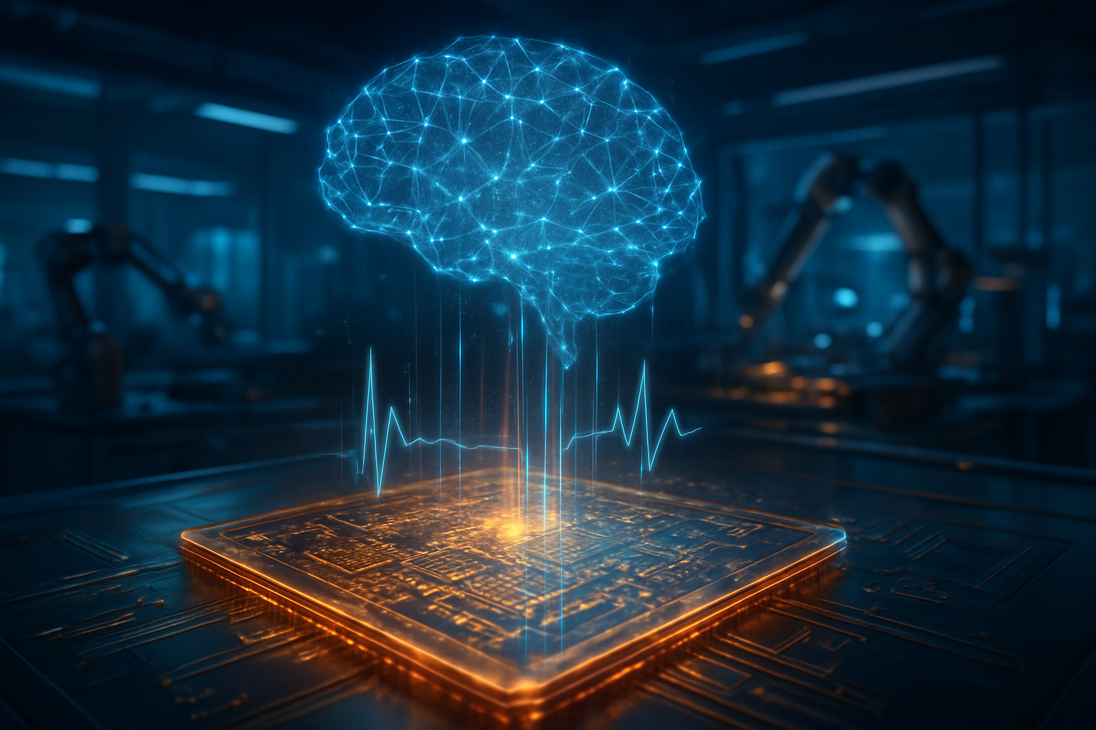
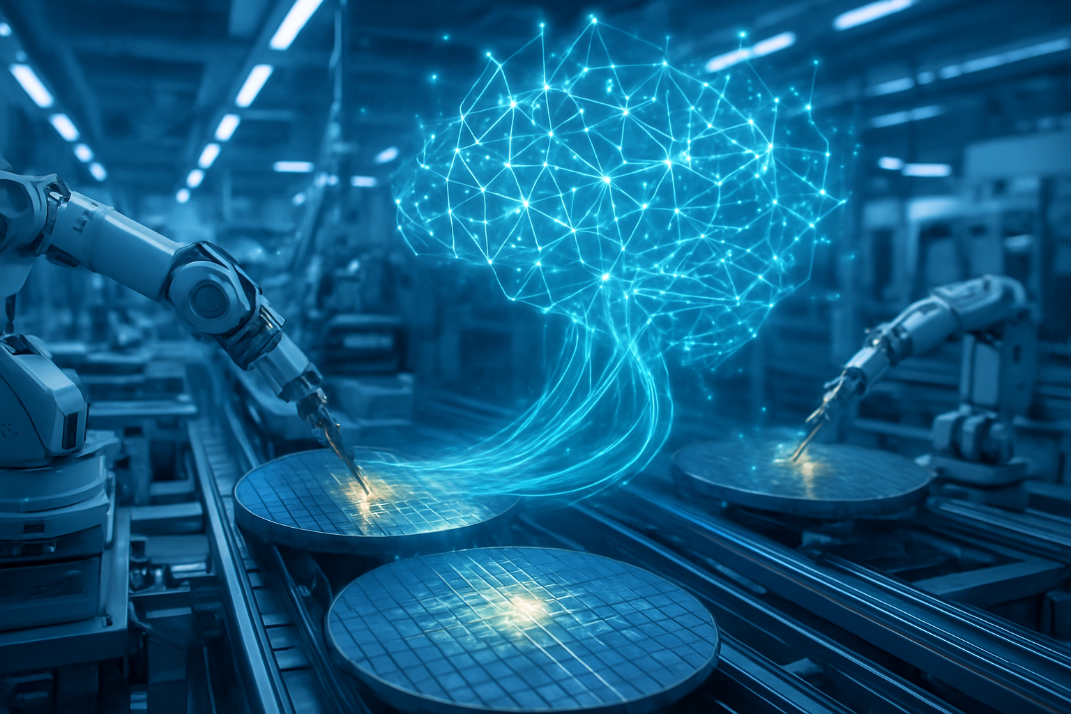
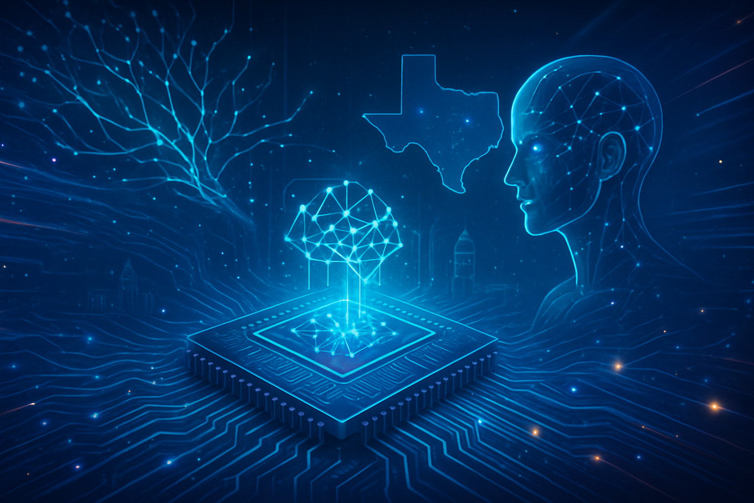
    In a landmark shift for the semiconductor industry, the dawn of 2026 has brought the "neuromorphic revolution" from the laboratory to the front lines of enterprise computing. Intel (NASDAQ: INTC) has officially transitioned its Loihi architecture into a new era of scale, moving beyond experimental prototypes to massive, billion-neuron systems that mimic the human brain’s biological efficiency. These systems, led by the flagship Hala Point cluster, are now demonstrating the ability to process complex AI sensory data and optimization workloads using 100 times less power than traditional high-end CPUs, marking a critical turning point in the global effort to make artificial intelligence sustainable.

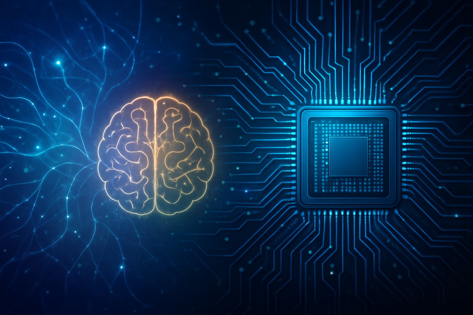
    This development arrives at a pivotal moment. As traditional data centers struggle under the massive energy demands of Large Language Models (LLMs) and generative AI, Intel’s neuromorphic advancements offer a radically different path. By processing information using "spikes"—discrete pulses of electricity that occur only when data changes—these chips eliminate the constant power draw inherent in conventional Von Neumann architectures. This efficiency isn't just a marginal gain; it is a fundamental reconfiguration of how machines think, allowing for real-time, continuous learning in devices ranging from autonomous drones to industrial robotics without the need for massive cooling systems or grid-straining power supplies.

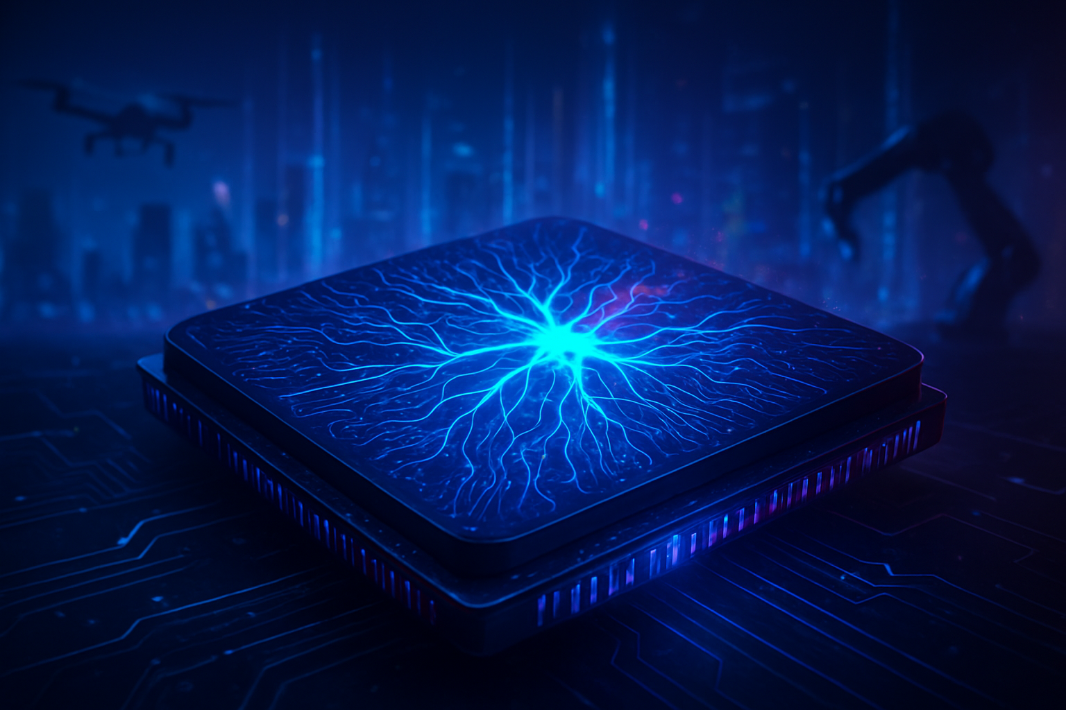
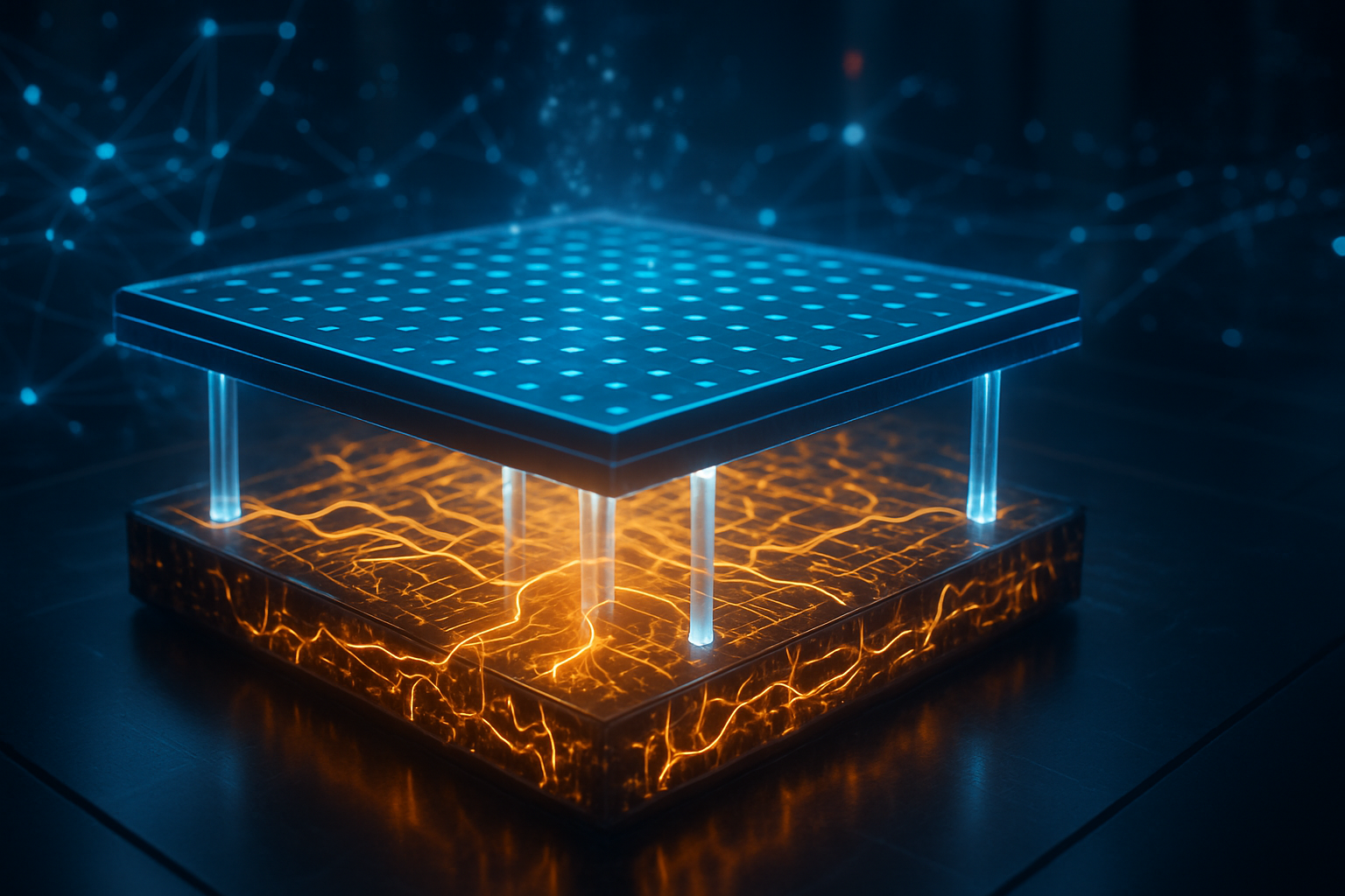
    The technical backbone of this breakthrough lies in the evolution of the Loihi 2 processor and its successor, the newly unveiled Loihi 3. While traditional chips are built around synchronized clocks and constant data movement between memory and the CPU, the Loihi 2 architecture integrates memory directly with processing logic at the "neuron" level. Each chip supports up to 1 million neurons and 120 million synapses, but the true innovation is in its "graded spikes." Unlike earlier neuromorphic designs that used simple binary on/off signals, these graded spikes allow for multi-dimensional data to be transmitted in a single pulse, vastly increasing the information density of the network while maintaining a microscopic power footprint.

    The scaling of these chips into the Hala Point system represents the pinnacle of current neuromorphic engineering. Hala Point integrates 1,152 Loihi 2 processors into a chassis no larger than a microwave oven, supporting a staggering 1.15 billion neurons and 128 billion synapses. This system achieves a performance metric of 20 quadrillion operations per second (petaops) with a peak power draw of only 2,600 watts. For comparison, achieving similar throughput on a traditional GPU-based cluster would require nearly 100 times that energy, often necessitating specialized liquid cooling.

    Industry experts have been quick to note the departure from "brute-force" AI. Dr. Mike Davies, director of Intel’s Neuromorphic Computing Lab, highlighted that while traditional AI models are essentially static after training, the Hala Point system supports "on-device learning," allowing the system to adapt to new environments in real-time. This capability has been validated by initial research from Sandia National Laboratories, where the hardware was used to solve complex optimization problems—such as real-time logistics and satellite pathfinding—at speeds that left modern server-grade processors in the dust.

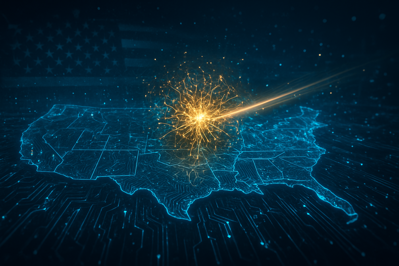
    The implications for the technology sector are profound, particularly for companies focused on "Edge AI" and robotics. Intel’s advancement places it in a unique competitive position against NVIDIA (NASDAQ: NVDA), which currently dominates the AI landscape through its high-powered H100 and B200 GPUs. While NVIDIA focuses on massive training clusters for LLMs, Intel is carving out a near-monopoly on high-efficiency inference and physical AI. This shift is likely to benefit firms specializing in autonomous systems, such as Tesla (NASDAQ: TSLA) and Boston Dynamics, who require immense on-board processing power without the weight and heat of traditional hardware.

    Furthermore, the emergence of IBM (NYSE: IBM) as a key player in the neuromorphic space with its NorthPole architecture and 3D Analog In-Memory Computing (AIMC) creates a two-horse race for the future of "Green AI." IBM's 2026 production-ready NorthPole chips are specifically targeting computer vision and Mixture-of-Experts (MoE) models, claiming energy efficiency gains of up to 1,000x for specific tasks. This competition is forcing a strategic pivot across the industry: major AI labs, once obsessed solely with model size, are now prioritizing "efficiency-first" architectures to lower the Total Cost of Ownership (TCO) for their enterprise clients.

    Startups like BrainChip (ASX: BRN) are also finding a foothold in this new ecosystem. By focusing on ultra-low-power "Akida" processors for IoT and automotive monitoring, these smaller players are proving that neuromorphic technology can be commercialized today, not just in a decade. As these efficient chips become more widely available, we can expect a disruption in the cloud service provider market; companies like Amazon (NASDAQ: AMZN) and Microsoft (NASDAQ: MSFT) may soon offer "Neuromorphic-as-a-Service" for clients whose workloads are too sensitive to latency or power costs for traditional cloud setups.

    The wider significance of the billion-neuron breakthrough cannot be overstated. For the past decade, the AI industry has been criticized for its "compute-at-any-cost" mentality, where the environmental impact of training a single model can equal the lifetime emissions of several automobiles. Neuromorphic computing directly addresses the "energy wall" that many predicted would stall AI progress. By proving that a system can simulate over a billion neurons with the power draw of a household appliance, Intel has demonstrated that AI growth does not have to be synonymous with environmental degradation.

    This milestone mirrors previous historic shifts in computing, such as the transition from vacuum tubes to transistors. In the same way that transistors allowed computers to move from entire rooms to desktops, neuromorphic chips are allowing high-level intelligence to move from massive data centers to the "edge" of the network. There are, however, significant hurdles. The software stack for neuromorphic chips—primarily Spiking Neural Networks (SNNs)—is fundamentally different from the backpropagation algorithms used in today’s deep learning. This creates a "programming gap" that requires a new generation of developers trained in event-based computing rather than traditional frame-based processing.

    Societal concerns also loom, particularly regarding privacy and security. If highly capable AI can run locally on a drone or a pair of glasses with 100x efficiency, the need for data to be sent to a central, regulated cloud diminishes. This could lead to a proliferation of untraceable, "always-on" AI surveillance tools that operate entirely off the grid. As the barrier to entry for high-performance AI drops, regulatory bodies will likely face new challenges in governing distributed, autonomous intelligence that doesn't rely on massive, easily-monitored data centers.

    Looking ahead, the next two years are expected to see the convergence of neuromorphic hardware with "Foundation Models." Researchers are already working on "Analog Foundation Models" that can run on Loihi 3 or IBM’s NorthPole with minimal accuracy loss. By 2027, experts predict we will see the first "Human-Scale" neuromorphic computer. Projects like DeepSouth at Western Sydney University are already aiming for 100 billion neurons—the approximate count of a human brain—using neuromorphic architectures to achieve real-time simulation speeds that were previously thought to be decades away.

    In the near term, the most immediate applications will be in scientific supercomputing and robotics. The development of the "NeuroFEM" algorithm allows these chips to solve partial differential equations (PDEs), which are used in everything from weather forecasting to structural engineering. This transforms neuromorphic chips from "AI accelerators" into general-purpose scientific tools. We can also expect to see "Hybrid AI" systems, where a traditional GPU handles the heavy lifting of training a model, while a neuromorphic chip like Loihi 3 handles the high-efficiency, real-time deployment and adaptation of that model in the physical world.

    Challenges remain, particularly in the standardization of hardware. Currently, an SNN designed for Intel hardware cannot easily run on IBM’s architecture. Industry analysts predict that the next 18 months will see a push for a "Universal Neuromorphic Language," similar to how CUDA standardized GPU programming. If the industry can agree on a common framework, the adoption of these billion-neuron systems could accelerate even faster than the current GPU-based AI boom.

    In summary, the advancements in Intel’s Loihi 2 and Loihi 3 architectures, and the operational success of the Hala Point system, represent a paradigm shift in artificial intelligence. By mimicking the architecture of the brain, Intel has solved the energy crisis that threatened to cap the potential of AI. The move to billion-neuron systems provides the scale necessary for truly intelligent, autonomous machines that can interact with the world in real-time, learning and adapting without the tether of a power cord or a data center connection.

    The significance of this development in AI history is likely to be viewed as the moment AI became "embodied." No longer confined to the digital vacuum of the cloud, intelligence is now moving into the physical fabric of our world. As we look toward the coming weeks, the industry will be watching for the first third-party benchmarks of the Loihi 3 chip and the announcement of more "Brain-Scale" systems. The era of brute-force AI is ending; the era of efficient, biological-scale intelligence has begun.


    This content is intended for informational purposes only and represents analysis of current AI developments.

    TokenRing AI delivers enterprise-grade solutions for multi-agent AI workflow orchestration, AI-powered development tools, and seamless remote collaboration platforms.
    For more information, visit https://www.tokenring.ai/.

  • The Brain-Like Revolution: Intel’s Loihi 3 and the Dawn of Real-Time Neuromorphic Edge AI

    The Brain-Like Revolution: Intel’s Loihi 3 and the Dawn of Real-Time Neuromorphic Edge AI

    The artificial intelligence industry is currently grappling with the staggering energy demands of traditional data centers. However, a paradigm shift is occurring at the "edge"—the point where digital intelligence meets the physical world. In a series of breakthrough announcements culminating in early 2026, Intel (NASDAQ: INTC) has unveiled its third-generation neuromorphic processor, Loihi 3, marking a definitive move away from power-hungry GPU architectures toward ultra-low-power, spike-based processing. This development, supported by high-profile collaborations with automotive leaders and aerospace agencies, signals that the era of "always-on" AI that mimics the human brain’s efficiency has officially arrived.

    Unlike the massive, energy-intensive Large Language Models (LLMs) that define the current AI landscape, these neuromorphic systems are designed for sub-millisecond reactions and extreme efficiency. By processing data as "spikes" of information only when changes occur—much like biological neurons—Intel and its competitors are enabling a new class of autonomous machines, from drones that can navigate dense forests at 80 km/h to prosthetic limbs that provide near-instant sensory feedback. This transition represents more than just a hardware upgrade; it is a fundamental reimagining of how machines perceive and interact with their environment in real time.

    A Technical Leap: Graded Spikes and 4nm Efficiency

    The release of Intel’s Loihi 3 in January 2026 represents a massive leap in capacity and architectural sophistication. Fabricated on a cutting-edge 4nm process, Loihi 3 packs 8 million neurons and 64 billion synapses per chip—an eightfold increase over the Loihi 2 architecture. The technical hallmark of this generation is the refinement of "graded spikes." While earlier neuromorphic chips relied on binary (on/off) signals, Loihi 3 utilizes up to 32-bit graded spikes. This allows the hardware to bridge the gap between traditional Deep Neural Networks (DNNs) and Spiking Neural Networks (SNNs), enabling developers to run mainstream AI workloads with a fraction of the power typically required by a GPU.

    At the core of this efficiency is the principle of temporal sparsity. Traditional chips, such as those produced by NVIDIA (NASDAQ: NVDA), process data in fixed frames, consuming power even when the scene is static. In contrast, Loihi 3 only activates the specific neurons required to process new, incoming events. This allows the chip to operate at a peak load of approximately 1.2 Watts, compared to the 300 Watts or more consumed by equivalent GPU-based systems for real-time inference. Furthermore, the integration of enhanced Spike-Timing-Dependent Plasticity (STDP) enables "on-chip learning," allowing robots to adapt to new physical conditions—such as a shift in a payload's weight—without needing to send data back to the cloud for retraining.

    The research community has reacted with significant enthusiasm, particularly following the 2024 deployment of "Hala Point," a massive neuromorphic system at Sandia National Laboratories. Utilizing over 1,000 Loihi processors to simulate 1.15 billion neurons, Hala Point demonstrated that neuromorphic architectures could achieve 15 TOPS/W (Tera-Operations Per Second per Watt) on standard AI benchmarks. Experts suggest that the commercialization of this scale in Loihi 3 marks the end of the "neuromorphic winter," proving that brain-inspired hardware can compete with and surpass silicon-standard architectures in specialized edge applications.

    Shifting the Competitive Landscape: Intel, IBM, and BrainChip

    The move toward neuromorphic dominance has ignited a fierce battle among tech giants and specialized startups. While Intel (NASDAQ: INTC) leads with its Loihi line, IBM (NYSE: IBM) has moved its "NorthPole" architecture into production for 2026. NorthPole differs from Loihi by co-locating memory and compute to eliminate the "von Neumann bottleneck," achieving up to 25 times the energy efficiency of an H100 GPU for image recognition tasks. This competitive pressure is forcing major AI labs to reconsider their hardware roadmaps, especially for products where battery life and heat dissipation are critical constraints, such as AR glasses and mobile robotics.

    Startups like BrainChip (ASX: BRN) are also gaining significant ground. In late 2025, BrainChip launched its Akida 2.0 architecture, which was notably licensed by NASA for use in space-grade AI applications where power is the most limited resource. BrainChip’s focus on "Temporal Event Neural Networks" (TENNs) has allowed it to secure a unique market position in "always-on" sensing, such as detecting anomalies in industrial machinery vibrations or EEG signals in healthcare. The strategic advantage for these companies lies in their ability to offer "intelligence at the source," reducing the need for expensive and latency-prone data transmissions to central servers.

    This disruption is already being felt in the automotive sector. Mercedes-Benz Group AG (OTC: MBGYY) has begun integrating neuromorphic vision systems for ultra-fast collision avoidance. By using event-based cameras that feed directly into neuromorphic processors, these vehicles can achieve a 0.1ms latency for pedestrian detection—far faster than the 30-50ms latency typical of frame-based systems. As these collaborations mature, traditional Tier-1 automotive suppliers may find their standard ECU (Engine Control Unit) offerings obsolete if they cannot integrate these specialized, low-latency AI accelerators.

    The Global Significance: Sustainability and the "Real-Time" AI Era

    The broader significance of the neuromorphic breakthrough extends to the very sustainability of the AI revolution. With global energy consumption from data centers projected to reach record highs, the "brute force" scaling of transformer models is hitting a wall of diminishing returns. Neuromorphic chips offer a "green" alternative for AI deployment, potentially reducing the carbon footprint of edge computing by orders of magnitude. This fits into a larger trend toward decentralized AI, where the goal is to move the "thinking" process out of the cloud and into the devices that actually interact with the physical world.

    However, the shift is not without concerns. The move toward brain-like processing brings up new challenges regarding the interpretability of AI. Spiking neural networks, by their nature, are more complex to "debug" than standard feed-forward networks because their state is dependent on time and history. Security experts have also raised questions about the potential for "adversarial spikes"—targeted inputs designed to exploit the temporal nature of these chips to cause malfunctions in autonomous systems. Despite these hurdles, the impact on fields like smart prosthetics and environmental monitoring is viewed as a net positive, enabling devices that can operate for months or years on a single charge.

    Comparisons are being drawn to the "AlexNet moment" in 2012, which launched the modern deep learning era. The successful commercialization of Loihi 3 and its peers is being called the "Neuromorphic Spring." For the first time, the industry has hardware that doesn't just run AI faster, but runs it differently, enabling applications—like sub-watt drone racing and adaptive medical implants—that were previously considered scientifically impossible with standard silicon.

    The Future: LLMs at the Edge and the Software Challenge

    Looking ahead, the next 18 to 24 months will likely focus on bringing Large Language Models to the edge via neuromorphic hardware. BrainChip recently secured $25 million in funding to commercialize "Akida GenAI," aiming to run 1.2-billion-parameter LLMs entirely on-device with minimal power draw. If successful, this would allow for truly private, offline AI assistants that reside in smartphones or home appliances without draining battery life or compromising user data. Near-term developments will also see the expansion of "hybrid" systems, where a traditional processor handles general tasks while a neuromorphic co-processor manages the high-speed sensory input.

    The primary challenge remaining is the software stack. Unlike the mature CUDA ecosystem developed by NVIDIA, neuromorphic programming models like Intel’s Lava are still in the process of gaining widespread developer adoption. Experts predict that the next major milestone will be the release of "compiler-agnostic" tools that allow developers to port PyTorch or TensorFlow models to neuromorphic hardware with a single click. Until this "ease-of-use" gap is closed, neuromorphic chips may remain limited to high-end industrial and research applications.

    Conclusion: A New Chapter in Silicon History

    The arrival of Intel’s Loihi 3 and the broader industry's pivot toward spike-based processing represents a historic milestone in the evolution of artificial intelligence. By successfully mimicking the efficiency and temporal nature of the biological brain, companies like Intel, IBM, and BrainChip have solved one of the most pressing problems in modern tech: how to deliver high-performance intelligence at the extreme edge of the network. The shift from power-hungry, frame-based processing to ultra-low-power, event-based "spikes" marks the beginning of a more sustainable and responsive AI future.

    As we move deeper into 2026, the industry should watch for the results of ongoing trials in autonomous transportation and the potential announcement of "Loihi-ready" consumer devices. The significance of this development cannot be overstated; it is the transition from AI that "calculates" to AI that "perceives." For the tech industry and society at large, the long-term impact will be felt in the seamless, silent integration of intelligence into every facet of our physical environment.


    This content is intended for informational purposes only and represents analysis of current AI developments.

    TokenRing AI delivers enterprise-grade solutions for multi-agent AI workflow orchestration, AI-powered development tools, and seamless remote collaboration platforms. For more information, visit https://www.tokenring.ai/.

  • The Great Flip: How Backside Power Delivery is Unlocking the Next Frontier of AI Compute

    The Great Flip: How Backside Power Delivery is Unlocking the Next Frontier of AI Compute

    The semiconductor industry has officially entered the "Angstrom Era," a transition marked by a radical architectural shift that flips the traditional logic of chip design upside down—quite literally. As of January 16, 2026, the long-anticipated deployment of Backside Power Delivery (BSPD) has moved from the research lab to high-volume manufacturing. Spearheaded by Intel (NASDAQ: INTC) and its PowerVia technology, followed closely by Taiwan Semiconductor Manufacturing Co. (NYSE: TSM) and its Super Power Rail (SPR) implementation, this breakthrough addresses the "interconnect bottleneck" that has threatened to stall AI performance gains for years. By moving the complex web of power distribution to the underside of the silicon wafer, manufacturers have finally "de-cluttered" the front side of the chip, paving the way for the massive transistor densities required by the next generation of generative AI models.

    The significance of this development cannot be overstated. For decades, chips were built like a house where the plumbing and electrical wiring were all crammed into the ceiling, leaving little room for the occupants (the signal-carrying wires). As transistors shrunk toward the 2nm and 1.6nm scales, this congestion led to "voltage droop" and thermal inefficiencies that limited clock speeds. With the successful ramp of Intel’s 18A node and TSMC’s A16 risk production this month, the industry has effectively moved the "plumbing" to the basement. This structural reorganization is not just a marginal improvement; it is the fundamental enabler for the thousand-teraflop chips that will power the AI revolution of the late 2020s.

    The Technical "De-cluttering": PowerVia vs. Super Power Rail

    At the heart of this shift is the physical separation of the Power Distribution Network (PDN) from the signal routing layers. Traditionally, both power and data traveled through the Back End of Line (BEOL), a stack of 15 to 20 metal layers atop the transistors. This led to extreme congestion, where bulky power wires consumed up to 30% of the available routing space on the most critical lower metal layers. Intel's PowerVia, the first to hit the market in the 18A node, solves this by using Nano-Through Silicon Vias (nTSVs) to route power from the backside of the wafer directly to the transistor layer. This has reduced "IR drop"—the loss of voltage due to resistance—from nearly 10% to less than 1%, ensuring that the billion-dollar AI clusters of 2026 can run at peak performance without the massive energy waste inherent in older architectures.

    TSMC’s approach, dubbed Super Power Rail (SPR) and featured on its A16 node, takes this a step further. While Intel uses nTSVs to reach the transistor area, TSMC’s SPR uses a more complex direct-contact scheme where the power network connects directly to the transistor’s source and drain. While more difficult to manufacture, early data from TSMC's 1.6nm risk production in January 2026 suggests this method provides a superior 10% speed boost and a 20% power reduction compared to its standard 2nm N2P process. This "de-cluttering" allows for a higher logic density—TSMC is currently targeting over 340 million transistors per square millimeter (MTr/mm²), cementing its lead in the extreme packaging required for high-performance computing (HPC).

    The industry’s reaction has been one of collective relief. For the past two years, AI researchers have expressed concern that the power-hungry nature of Large Language Models (LLMs) would hit a thermal ceiling. The arrival of BSPD has largely silenced these fears. By evacuating the signal highway of power-related clutter, chip designers can now use wider signal traces with less resistance, or more tightly packed traces with less crosstalk. The result is a chip that is not only faster but significantly cooler, allowing for higher core counts in the same physical footprint.

    The AI Foundry Wars: Who Wins the Angstrom Race?

    The commercial implications of BSPD are reshaping the competitive landscape between major AI labs and hardware giants. NVIDIA (NASDAQ: NVDA) remains the primary beneficiary of TSMC’s SPR technology. While NVIDIA’s current "Rubin" platform relies on mature 3nm processes for volume, reports indicate that its upcoming "Feynman" GPU—the anticipated successor slated for late 2026—is being designed from the ground up to leverage TSMC’s A16 node. This will allow NVIDIA to maintain its dominance in the AI training market by offering unprecedented compute-per-watt metrics that competitors using traditional frontside delivery simply cannot match.

    Meanwhile, Intel’s early lead in bringing PowerVia to high-volume manufacturing has transformed its foundry business. Microsoft (NASDAQ: MSFT) has confirmed it is utilizing Intel’s 18A node for its next-generation "Maia 3" AI accelerators, specifically citing the efficiency gains of PowerVia as the deciding factor. By being the first to cross the finish line with a functional BSPD node, Intel has positioned itself as a viable alternative to TSMC for companies like Advanced Micro Devices (NASDAQ: AMD) and Apple (NASDAQ: AAPL), who are looking for geographical diversity in their supply chains. Apple, in particular, is rumored to be testing Intel’s 18A for its mid-range chips while reserving TSMC’s A16 for its flagship 2027 iPhone processors.

    The disruption extends beyond the foundries. As BSPD becomes the standard, the entire Electronic Design Automation (EDA) software market has had to pivot. Tools from companies like Cadence and Synopsys have been completely overhauled to handle "double-sided" chip design. This shift has created a barrier to entry for smaller chip startups that lack the sophisticated design tools and R&D budgets to navigate the complexities of backside routing. In the high-stakes world of AI, the move to BSPD is effectively raising the "table stakes" for entry into the high-end compute market.

    Beyond the Transistor: BSPD and the Global AI Landscape

    In the broader context of the AI landscape, Backside Power Delivery is the "invisible" breakthrough that makes everything else possible. As generative AI moves from simple text generation to real-time multimodal interaction and scientific simulation, the demand for raw compute is scaling exponentially. BSPD is the key to meeting this demand without requiring a tripling of global data center energy consumption. By improving performance-per-watt by as much as 20% across the board, this technology is a critical component in the tech industry’s push toward environmental sustainability in the face of the AI boom.

    Comparisons are already being made to the 2011 transition from planar transistors to FinFETs. Just as FinFETs allowed the smartphone revolution to continue by curbing leakage current, BSPD is the gatekeeper for the next decade of AI progress. However, this transition is not without concerns. The manufacturing process for BSPD involves extreme wafer thinning and bonding—processes where the silicon is ground down to a fraction of its original thickness. This introduces new risks in yield and structural integrity, which could lead to supply chain volatility if foundries hit a snag in scaling these delicate procedures.

    Furthermore, the move to backside power reinforces the trend of "silicon sovereignty." Because BSPD requires such specialized manufacturing equipment—including High-NA EUV lithography and advanced wafer bonding tools—the gap between the top three foundries (TSMC, Intel, and Samsung Electronics (KRX: 005930)) and the rest of the world is widening. Samsung, while slightly behind Intel and TSMC in the BSPD race, is currently ramping its SF2 node and plans to integrate full backside power in its SF2Z node by 2027. This technological "moat" ensures that the future of AI will remain concentrated in a handful of high-tech hubs.

    The Horizon: Backside Signals and the 1.4nm Future

    Looking ahead, the successful implementation of backside power is only the first step. Experts predict that by 2028, we will see the introduction of "Backside Signal Routing." Once the infrastructure for backside power is in place, designers will likely begin moving some of the less-critical signal wires to the back of the wafer as well, further de-cluttering the front side and allowing for even more complex transistor architectures. This would mark the complete transition of the silicon wafer from a single-sided canvas to a fully three-dimensional integrated circuit.

    In the near term, the industry is watching for the first "live" benchmarks of the Intel Clearwater Forest (Xeon 6+) server chips, which will be the first major data center processors to utilize PowerVia at scale. If these chips meet their aggressive performance targets in the first half of 2026, it will validate Intel’s roadmap and likely trigger a wave of migration from legacy frontside designs. The real test for TSMC will come in the second half of the year as it attempts to bring the complex A16 node into high-volume production to meet the insatiable demand from the AI sector.

    Challenges remain, particularly in the realm of thermal management. While BSPD makes the chip more efficient, it also changes how heat is dissipated. Since the backside is now covered in a dense metal power grid, traditional cooling methods that involve attaching heat sinks directly to the silicon substrate may need to be redesigned. Experts suggest that we may see the rise of "active" backside cooling or integrated liquid cooling channels within the power delivery network itself as we approach the 1.4nm node era in late 2027.

    Conclusion: Flipping the Future of AI

    The arrival of Backside Power Delivery marks a watershed moment in semiconductor history. By solving the "clutter" problem on the front side of the wafer, Intel and TSMC have effectively broken through a physical wall that threatened to halt the progress of Moore’s Law. As of early 2026, the transition is well underway, with Intel’s 18A leading the charge into consumer and enterprise products, and TSMC’s A16 promising a performance ceiling that was once thought impossible.

    The key takeaway for the tech industry is that the AI hardware of the future will not just be about smaller transistors, but about smarter architecture. The "Great Flip" to backside power has provided the industry with a renewed lease on performance growth, ensuring that the computational needs of ever-larger AI models can be met through the end of the decade. For investors and enthusiasts alike, the next 12 months will be critical to watch as these first-generation BSPD chips face the rigors of real-world AI workloads. The Angstrom Era has begun, and the world of compute will never look the same—front or back.


    This content is intended for informational purposes only and represents analysis of current AI developments.

    TokenRing AI delivers enterprise-grade solutions for multi-agent AI workflow orchestration, AI-powered development tools, and seamless remote collaboration platforms.
    For more information, visit https://www.tokenring.ai/.

  • Federal Preemption: President Trump Signs Landmark AI Executive Order to Dismantle State Regulations

    Federal Preemption: President Trump Signs Landmark AI Executive Order to Dismantle State Regulations

    In a move that has sent shockwaves through both Silicon Valley and state capitals across the country, President Trump signed the "Executive Order on Ensuring a National Policy Framework for Artificial Intelligence" on December 11, 2025. Positioned as the cornerstone of the administration’s "America First AI" strategy, the order seeks to fundamentally reshape the regulatory landscape by establishing a single, deregulatory federal standard for artificial intelligence. By explicitly moving to supersede state-level safety and transparency laws, the White House aims to eliminate what it describes as a "burdensome patchwork" of regulations that threatens to hinder American technological dominance.

    The immediate significance of this directive cannot be overstated. As of January 12, 2026, the order has effectively frozen the enforcement of several landmark state laws, most notably in California and Colorado. By asserting federal authority over "Frontier AI" models under the Dormant Commerce Clause, the administration is betting that a unified, "innovation-first" approach will provide the necessary velocity for U.S. companies to outpace global competitors, particularly China, in the race for Artificial General Intelligence (AGI).

    A "One Federal Standard" Doctrine for the Frontier

    The Executive Order introduces a "One Federal Standard" doctrine, which argues that because AI models are developed and deployed across state lines, they constitute "inherent instruments of interstate commerce." This legal framing is designed to strip states of their power to mandate independent safety testing, bias mitigation, or reporting requirements. Specifically, the order targets California’s stringent transparency laws and Colorado’s Consumer Protections in Interactions with AI Act, labeling them as "onerous barriers" to progress. In a sharp reversal of previous policy, the order also revokes the remaining reporting requirements of the Biden-era EO 14110, replacing prescriptive safety mandates with "minimally burdensome" voluntary partnerships.

    Technically, the order shifts the focus from "safety-first" precautionary measures to "truth-seeking" and "ideological neutrality." A key provision requires federal agencies to ensure that AI models are not "engineered" to prioritize Diversity, Equity, and Inclusion (DEI) metrics over accuracy. This "anti-woke" mandate prohibits the government from procuring or requiring models that have been fine-tuned with specific ideological filters, which the administration claims distort the "objective reasoning" of large language models. Furthermore, the order streamlines federal permitting for AI data centers, bypassing certain environmental review hurdles for projects deemed critical to national security—a move intended to accelerate the deployment of massive compute clusters.

    Initial reactions from the AI research community have been starkly divided. While "accelerationists" have praised the removal of bureaucratic red tape, safety-focused researchers at organizations like the Center for AI Safety warn of a "safety vacuum." They argue that removing state-level guardrails without a robust federal replacement could lead to the deployment of unvetted models with catastrophic potential. However, hardware researchers have largely welcomed the permitting reforms, noting that power and infrastructure constraints are currently the primary bottlenecks to advancing model scale.

    Silicon Valley Divided: Winners and Losers in the New Regime

    The deregulatory shift has found enthusiastic support among the industry’s biggest players. Nvidia (NASDAQ: NVDA), the primary provider of the hardware powering the AI revolution, has seen its strategic position bolstered by the order’s focus on rapid infrastructure expansion. Similarly, OpenAI (supported by Microsoft (NASDAQ: MSFT)) and xAI (led by Elon Musk) have voiced strong support for a unified federal standard. Sam Altman of OpenAI, who has transitioned into a frequent advisor for the administration, emphasized that a single regulatory framework is vital for the $500 billion AI infrastructure push currently underway.

    Venture capital firms, most notably Andreessen Horowitz (a16z), have hailed the order as a "death blow" to the "decelerationist" movement. By preempting state laws, the order protects smaller startups from the prohibitive legal costs associated with complying with 50 different sets of state regulations. This creates a strategic advantage for U.S.-based labs, allowing them to iterate faster than their European counterparts, who remain bound by the comprehensive EU AI Act. However, tech giants like Alphabet (NASDAQ: GOOGL) and Meta Platforms (NASDAQ: META) now face a complex transition period as they navigate the "shadow period" of enforcement while state-level legal challenges play out in court.

    The disruption to existing products is already visible. Companies that had spent the last year engineering models to comply with California’s specific safety and bias requirements are now forced to decide whether to maintain those filters or pivot to the new "ideological neutrality" standards to remain eligible for federal contracts. This shift in market positioning could favor labs that have historically leaned toward "open" or "unfiltered" models, potentially marginalizing those that have built their brands around safety-centric guardrails.

    The Constitutional Clash and the "America First" Vision

    The wider significance of the December 2025 EO lies in its aggressive use of federal power to dictate the cultural and technical direction of AI. By leveraging the Spending Clause, the administration has threatened to withhold billions in Broadband Equity Access and Deployment (BEAD) funds from states that refuse to suspend their own AI regulations. California, for instance, currently has approximately $1.8 billion in infrastructure grants at risk. This "carrot and stick" approach represents a significant escalation in the federal government’s attempt to centralize control over emerging technologies.

    The battle is not just over safety, but over the First Amendment. The administration argues that state laws requiring "bias audits" or "safety filters" constitute "compelled speech" and "viewpoint discrimination" against developers. This legal theory, if upheld by the Supreme Court, could redefine the relationship between the government and software developers for decades. Critics, including California Governor Gavin Newsom and Attorney General Rob Bonta, have decried the order as "federal overreach" that sacrifices public safety for corporate profit, setting the stage for a landmark constitutional showdown.

    Historically, this event marks a definitive pivot away from the global trend of increasing AI regulation. While the EU and several U.S. states were moving toward a "precautionary principle" model, the Trump administration has effectively doubled down on "technological exceptionalism." This move draws comparisons to the early days of the internet, where light-touch federal regulation allowed U.S. companies to dominate the global web, though opponents argue that the existential risks of AI make such a comparison dangerous.

    The Horizon: Legal Limbo and the Compute Boom

    In the near term, the AI industry is entering a period of significant legal uncertainty. While the Department of Justice’s new AI Litigation Task Force has already begun filing "Statements of Interest" in state cases, many companies are caught in a "legal limbo." They face the risk of losing federal funding if they comply with state laws, yet they remain liable under those same state laws until a definitive court ruling is issued. Legal experts predict that the case will likely reach the Supreme Court by late 2026, making this the most watched legal battle in the history of the tech industry.

    Looking further ahead, the permitting reforms included in the EO are expected to trigger a massive boom in data center construction across the "Silicon Heartland." With environmental hurdles lowered, companies like Amazon (NASDAQ: AMZN) and Oracle (NYSE: ORCL) are expected to accelerate their multi-billion dollar investments in domestic compute clusters. This infrastructure surge is intended to ensure that the next generation of AGI is "Made in America," regardless of the environmental or local regulatory costs.

    Final Thoughts: A New Era of AI Geopolitics

    President Trump’s December 2025 Executive Order represents one of the most consequential shifts in technology policy in American history. By choosing to preempt state laws and prioritize innovation over precautionary safety, the administration has signaled that it views the AI race as a zero-sum geopolitical struggle. The key takeaway for the industry is clear: the federal government is now the primary arbiter of AI development, and its priority is speed and "ideological neutrality."

    The significance of this development will be measured by its ability to withstand the coming wave of litigation. If the "One Federal Standard" holds, it will provide U.S. AI labs with a regulatory environment unlike any other in the world—one designed specifically to facilitate the rapid scaling of intelligence. In the coming weeks and months, the industry will be watching the courts and the first "neutrality audits" from the FTC to see how this new framework translates from executive decree into operational reality.


    This content is intended for informational purposes only and represents analysis of current AI developments.

    TokenRing AI delivers enterprise-grade solutions for multi-agent AI workflow orchestration, AI-powered development tools, and seamless remote collaboration platforms.
    For more information, visit https://www.tokenring.ai/.

  • High-NA EUV Era Begins: Intel Deploys First ASML Tool as China Signals EUV Prototype Breakthrough

    High-NA EUV Era Begins: Intel Deploys First ASML Tool as China Signals EUV Prototype Breakthrough

    The global semiconductor landscape reached a historic inflection point in late 2025 as Intel Corporation (NASDAQ: INTC) announced the successful installation and acceptance testing of the industry's first commercial High-Numerical Aperture (High-NA) Extreme Ultraviolet (EUV) lithography tool. The machine, a $350 million ASML (NASDAQ: ASML) Twinscan EXE:5200B, represents the most advanced piece of manufacturing equipment ever created, signaling the start of the "Angstrom Era" in chip production. By securing the first of these massive systems, Intel aims to leapfrog its rivals and reclaim the crown of transistor density and power efficiency.

    However, the Western technological lead is facing an unprecedented challenge from the East. Simultaneously, reports have emerged from Shenzhen, China, indicating that a domestic research consortium has validated a working EUV prototype. This breakthrough, part of a state-sponsored "Manhattan Project" for semiconductors, suggests that China is making rapid progress in bypassing US-led export bans. While the Chinese prototype is not yet ready for high-volume manufacturing, its existence marks a significant milestone in Beijing’s quest for technological sovereignty, with a stated goal of producing domestic EUV-based processors by 2028.

    The Technical Frontier: 1.4nm and the High-NA Advantage

    The ASML Twinscan EXE:5200B is a marvel of engineering, standing nearly two stories tall and requiring multiple Boeing 747s for transport. The defining feature of this tool is its Numerical Aperture (NA), which has been increased from the 0.33 of standard EUV machines to 0.55. This jump in NA allows for an 8nm resolution, a significant improvement over the 13.5nm limit of previous generations. For Intel, this means the ability to print features for its upcoming 14A (1.4nm) node using "single-patterning." Previously, achieving such small dimensions required "multi-patterning," a process where a single layer is printed multiple times, which increases the risk of defects and dramatically raises production costs.

    Initial reactions from the semiconductor research community have been a mix of awe and cautious optimism. Dr. Aris Silzars, a veteran industry analyst, noted that the EXE:5200B’s throughput—capable of processing 175 to 200 wafers per hour—is the "holy grail" for making the 1.4nm node economically viable. The tool also boasts an overlay accuracy of 0.7 nanometers, a precision equivalent to hitting a golf ball on the moon from Earth. Experts suggest that by adopting High-NA early, Intel is effectively "de-risking" its roadmap for the next decade, while competitors like Taiwan Semiconductor Manufacturing Company (NYSE: TSM) and Samsung Electronics (KRX: 005930) have opted for a more conservative approach, extending the life of standard EUV tools through complex multi-patterning techniques.

    In contrast, the Chinese prototype developed in Shenzhen utilizes a different technical path. While ASML uses Laser-Produced Plasma (LPP) to generate EUV light, the Chinese team, reportedly led by engineers from Huawei and various state-funded institutes, has successfully demonstrated a Laser-Induced Discharge Plasma (LDP) source. Though currently producing only 100W–150W of power—roughly half of what is needed for high-speed commercial production—it proves that China has solved the fundamental physics of EUV light generation. This "Manhattan Project" approach has involved a massive mobilization of talent, including former ASML and Nikon (OTC: NINNY) engineers, to reverse-engineer the complex reflective optics and light sources that were previously thought to be decades out of reach for domestic Chinese firms.

    Strategic Maneuvers: The Battle for Lithography Leadership

    Intel’s aggressive move to install the EXE:5200B is a clear strategic play to regain the manufacturing lead it lost over the last decade. By being the first to master High-NA, Intel (NASDAQ: INTC) provides its foundry customers with a unique value proposition: the ability to manufacture the world’s most advanced AI and mobile chips with fewer processing steps and higher yields. This development puts immense pressure on TSMC (NYSE: TSM), which has dominated the 3nm and 5nm markets. If Intel can successfully ramp up the 14A node by 2026 or 2027, it could disrupt the current foundry hierarchy and attract major clients like Apple and Nvidia that have traditionally relied on Taiwanese fabrication.

    The competitive implications extend far beyond the United States and Taiwan. China's breakthrough in Shenzhen represents a direct challenge to the efficacy of the U.S. Department of Commerce's export controls. For years, the denial of EUV tools to Chinese firms like SMIC was considered a "hard ceiling" that would prevent China from progressing beyond the 7nm or 5nm nodes. The validation of a domestic EUV prototype suggests that this ceiling is cracking. If China can scale this technology, it would not only secure its own supply chain but also potentially offer a cheaper, state-subsidized alternative to the global market, disrupting the high-margin business models of Western equipment makers.

    Furthermore, the emergence of the Chinese "Manhattan Project" has sparked a new arms race in lithography. Companies like Canon (NYSE: CAJ) are attempting to bypass EUV altogether with "nanoimprint" lithography, but the industry consensus remains that EUV is the only viable path for sub-2nm chips. Intel’s first-mover advantage with the EXE:5200B creates a "financial and technical moat" that may be too expensive for smaller players to cross, potentially consolidating the leading-edge market into a triopoly of Intel, TSMC, and Samsung.

    Geopolitical Stakes and the Future of Moore’s Law

    The simultaneous announcements from Oregon and Shenzhen highlight the intensifying "Chip War" between the U.S. and China. This is no longer just a corporate competition; it is a matter of national security and economic survival. The High-NA EUV tools are the "printing presses" of the modern era, and the nation that controls them controls the future of Artificial Intelligence, autonomous systems, and advanced weaponry. Intel's success is seen as a validation of the CHIPS Act and the U.S. strategy to reshore critical manufacturing.

    However, the broader AI landscape is also at stake. As AI models grow in complexity, the demand for more transistors per square millimeter becomes insatiable. High-NA EUV is the only technology currently capable of sustaining the pace of Moore’s Law—the observation that the number of transistors on a microchip doubles about every two years. Without the precision of the EXE:5200B, the industry would likely face a "performance wall," where the energy costs of running massive AI data centers would become unsustainable.

    The potential concerns surrounding this development are primarily geopolitical. If China succeeds in its 2028 goal of domestic EUV processors, it could render current sanctions obsolete and lead to a bifurcated global tech ecosystem. We are witnessing the end of a globalized semiconductor supply chain and the birth of two distinct, competing stacks: one led by the U.S. and ASML, and another led by China’s centralized "whole-of-nation" effort. This fragmentation could lead to higher costs for consumers and a slower pace of global innovation as research is increasingly siloed behind national borders.

    The Road to 2028: What Lies Ahead

    Looking forward, the next 24 to 36 months will be critical for both Intel and the Chinese consortium. For Intel (NASDAQ: INTC), the challenge is transitioning from "installation" to "yield." It is one thing to have a $350 million machine; it is another to produce millions of perfect chips with it. The industry will be watching closely for the first "tape-outs" of the 14A node, which will serve as the litmus test for High-NA's commercial viability. If Intel can prove that High-NA reduces the total cost of ownership per transistor, it will have successfully executed one of the greatest comebacks in industrial history.

    In China, the focus will shift from the Shenzhen prototype to the more ambitious "Steady-State Micro-Bunching" (SSMB) project in Xiong'an. Unlike the standalone ASML tools, SSMB uses a particle accelerator to generate EUV light for an entire cluster of lithography machines. If this centralized light-source model works, it could fundamentally change the economics of chipmaking, allowing China to build "EUV factories" that are more scalable than anything in the West. Experts predict that while 2028 is an aggressive target for domestic EUV processors, a 2030 timeline for stable production is increasingly realistic.

    The immediate challenges remain daunting. For Intel, the "reticle stitching" required by High-NA’s smaller field size presents a significant software and design hurdle. For China, the lack of a mature ecosystem for EUV photoresists and masks—the specialized chemicals and plates used in the printing process—could still stall their progress even if the light source is perfected. The race is now a marathon of engineering endurance.

    Conclusion: A New Chapter in Silicon History

    The installation of the ASML Twinscan EXE:5200B at Intel and the emergence of China’s EUV prototype represent the start of a new chapter in silicon history. We have officially moved beyond the era where 0.33 NA lithography was the pinnacle of human achievement. The "High-NA Era" promises to push computing power to levels previously thought impossible, enabling the next generation of AI breakthroughs that will define the late 2020s and beyond.

    As we move into 2026, the significance of these developments cannot be overstated. Intel has reclaimed a seat at the head of the technical table, but China has proven that it will not be easily sidelined. The "Manhattan Project" for chips is no longer a theoretical threat; it is a functional reality that is beginning to produce results. The long-term impact will be a world where the most advanced technology is both a tool for incredible progress and a primary instrument of geopolitical power.

    In the coming weeks and months, industry watchers should look for announcements regarding Intel's first 14A test chips and any further technical disclosures from the Shenzhen research group. The battle for the 1.4nm node has begun, and the stakes have never been higher.


    This content is intended for informational purposes only and represents analysis of current AI developments.

    TokenRing AI delivers enterprise-grade solutions for multi-agent AI workflow orchestration, AI-powered development tools, and seamless remote collaboration platforms.
    For more information, visit https://www.tokenring.ai/.

  • The Power Behind the Processing: OSU’s Anant Agarwal Elected to NAI for Semiconductor Breakthroughs

    The Power Behind the Processing: OSU’s Anant Agarwal Elected to NAI for Semiconductor Breakthroughs

    The National Academy of Inventors (NAI) has officially named Dr. Anant Agarwal, a Professor of Electrical and Computer Engineering at The Ohio State University (OSU), to its prestigious Class of 2025. This election marks a pivotal recognition of Agarwal’s decades-long work in wide-bandgap (WBG) semiconductors—specifically Silicon Carbide (SiC) and Gallium Nitride (GaN)—which have become the unsung heroes of the modern artificial intelligence revolution. As AI models grow in complexity, the hardware required to train and run them has hit a "power wall," and Agarwal’s innovations provide the critical efficiency needed to scale these systems sustainably.

    The significance of this development cannot be overstated as the tech industry grapples with the massive energy demands of next-generation data centers. While much of the public's attention remains on the logic chips designed by companies like NVIDIA (NASDAQ:NVDA), the power electronics that deliver electricity to those chips are often the limiting factor in performance and density. Dr. Agarwal’s election to the NAI highlights a shift in the AI hardware narrative: the most important breakthroughs are no longer just about how we process data, but how we manage the massive amounts of energy required to do so.

    Revolutionizing Power with Silicon Carbide and AI-Driven Screening

    Dr. Agarwal’s work at the SiC Power Devices Reliability Lab at OSU focuses on the "ruggedness" and reliability of Silicon Carbide MOSFETs, which are capable of operating at much higher voltages, temperatures, and frequencies than traditional silicon. A primary technical challenge in SiC technology has been the instability of the gate oxide layer, which often leads to device failure under the high-stress environments typical of AI server racks. Agarwal’s team has pioneered a threshold voltage adjustment technique using low-field pulses, effectively stabilizing the devices and ensuring they can handle the volatile power cycles of high-performance computing.

    Perhaps the most groundbreaking technical advancement from Agarwal’s lab in the 2024-2025 period is the development of an Artificial Neural Network (ANN)-based screening methodology for semiconductor manufacturing. Traditional testing methods for SiC MOSFETs often involve destructive testing or imprecise statistical sampling. Agarwal’s new approach uses machine learning to predict the Short-Circuit Withstand Time (SCWT) of individual packaged chips. This allows manufacturers to identify and discard "weak" chips that might otherwise fail after a few months in a data center, reducing field failure rates from several percentage points to parts-per-million levels.

    Furthermore, Agarwal is pushing the boundaries of "smart" power chips through SiC CMOS technology. By integrating both N-channel and P-channel MOSFETs on a single SiC die, his research has enabled power chips that can operate at voltages exceeding 600V while maintaining six times the power density of traditional silicon. This allows for a massive reduction in the physical size of power supplies, a critical requirement for the increasingly cramped environments of AI-optimized server blades.

    Strategic Impact on the Semiconductor Giants and AI Infrastructure

    The commercial implications of Agarwal’s research are already being felt across the semiconductor industry. Companies like Wolfspeed (NYSE:WOLF), where Agarwal previously served as a technical leader, stand to benefit from the increased reliability and yield of SiC wafers. As the industry moves toward 200mm wafer production, the ANN-based screening techniques developed at OSU provide a competitive edge in maintaining quality control at scale. Major power semiconductor players, including ON Semiconductor (NASDAQ:ON) and STMicroelectronics (NYSE:STM), are also closely watching these developments as they race to supply the power-hungry AI market.

    For AI giants like NVIDIA and Google (NASDAQ:GOOGL), the adoption of Agarwal’s high-density power conversion technology is a strategic necessity. Current AI GPUs require hundreds of amps of current at very low voltages (often around 1V). Converting power from the 48V or 400V DC rails of a modern data center down to the 1V required by the chip is traditionally an inefficient process that generates immense heat. By using the 3.3 kV and 1.2 kV SiC MOSFETs commercialized through Agarwal’s spin-out, NoMIS Power, data centers can achieve higher-frequency switching, which significantly reduces the size of transformers and capacitors, allowing for more compute density per rack.

    This shift disrupts the existing cooling and power delivery market. Traditional liquid cooling providers and power module manufacturers are having to pivot as SiC-based systems can operate at junction temperatures up to 200°C. This thermal resilience allows for air-cooled power modules in environments that previously required expensive and complex liquid cooling setups, potentially lowering the capital expenditure for new AI startups and mid-sized data center operators.

    The Broader AI Landscape: Efficiency as the New Frontier

    Dr. Agarwal’s innovations fit into a broader trend where energy efficiency is becoming the primary metric for AI success. For years, the industry followed "Moore’s Law" for logic, but power electronics lagged behind. We are now entering what experts call the "Second Electronics Revolution," moving from the Silicon Age to the Wide-Bandgap Age. This transition is essential for the "decarbonization" of AI; without the efficiency gains provided by SiC and GaN, the carbon footprint of global AI training would likely become ecologically and politically untenable.

    The wider significance also touches on national security and domestic manufacturing. Through his leadership in PowerAmerica, Agarwal has been instrumental in ensuring the United States maintains a robust supply chain for wide-bandgap semiconductors. As geopolitical tensions influence the semiconductor trade, the ability to manufacture high-reliability power electronics domestically at OSU and through partners like Wolfspeed provides a strategic safeguard for the U.S. tech economy.

    However, the rapid transition to SiC is not without concerns. The manufacturing process for SiC is significantly more energy-intensive and complex than for standard silicon. While Agarwal’s work improves the reliability and usage efficiency, the industry still faces a steep curve in scaling the raw material production. Comparisons are often made to the early days of the microprocessor revolution—we are currently in the "scaling" phase of power semiconductors, where the innovations of today will determine the infrastructure of the next thirty years.

    Future Horizons: Smart Chips and 3.3kV AI Rails

    Looking ahead to 2026 and beyond, the industry expects a surge in the adoption of 3.3 kV SiC MOSFETs for AI power rails. NoMIS Power’s recent launch of these devices in late 2025 is just the beginning. Near-term developments will likely focus on integrating Agarwal's ANN-based screening directly into the automated test equipment (ATE) used by global chip foundries. This would standardize "reliability-as-a-service" for any company purchasing SiC-based power modules.

    On the horizon, we may see the emergence of "autonomous power modules"—chips that use Agarwal’s SiC CMOS technology to monitor their own health and adjust their operating parameters in real-time to prevent failure. Such "self-healing" hardware would be a game-changer for edge AI applications, such as autonomous vehicles and remote satellite systems, where manual maintenance is impossible. Experts predict that the next five years will see SiC move from a "premium" alternative to the baseline standard for all high-performance computing power delivery.

    A Legacy of Innovation and the Path Forward

    Dr. Anant Agarwal’s election to the National Academy of Inventors is a well-deserved recognition of a career that has bridged the gap between fundamental physics and industrial application. From his early days at Cree to his current leadership at Ohio State, his focus on the "ruggedness" of technology has ensured that the AI revolution is built on a stable and efficient foundation. The key takeaway for the industry is clear: the future of AI is as much about the power cord as it is about the processor.

    As we move into 2026, the tech community should watch for the results of the first large-scale deployments of ANN-screened SiC modules in hyperscale data centers. If these devices deliver the promised reduction in failure rates and energy overhead, they will solidify SiC as the bedrock of the AI era. Dr. Agarwal’s work serves as a reminder that true innovation often happens in the layers of technology we rarely see, but without which the digital world would grind to a halt.


    This content is intended for informational purposes only and represents analysis of current AI developments.

    TokenRing AI delivers enterprise-grade solutions for multi-agent AI workflow orchestration, AI-powered development tools, and seamless remote collaboration platforms.
    For more information, visit https://www.tokenring.ai/.

  • Beyond Silicon: A Materials Science Revolution Reshaping the Future of Chip Design

    Beyond Silicon: A Materials Science Revolution Reshaping the Future of Chip Design

    The relentless march of technological progress, particularly in artificial intelligence (AI), 5G/6G communication, electric vehicles, and the burgeoning Internet of Things (IoT), is pushing the very limits of traditional silicon-based electronics. As Moore's Law, which has guided the semiconductor industry for decades, begins to falter, a quiet yet profound revolution in materials science is taking center stage. New materials, with their extraordinary electrical, thermal, and mechanical properties, are not merely incremental improvements; they are fundamentally redefining what's possible in chip design, promising a future of faster, smaller, more energy-efficient, and functionally diverse electronic devices. This shift is critical for sustaining the pace of innovation, addressing the escalating demands of modern computing, and overcoming the inherent physical and economic constraints that silicon now presents.

    The immediate significance of this materials science revolution is multifaceted. It promises continued miniaturization and unprecedented performance enhancements, enabling denser and more powerful chips than ever before. Critically, many of these novel materials inherently consume less power and generate less heat, directly addressing the critical need for extended battery life in mobile devices and substantial energy reductions in vast data centers. Beyond traditional computing metrics, these materials are unlocking entirely new functionalities, from flexible electronics and advanced sensors to neuromorphic computing architectures and robust high-frequency communication systems, laying the groundwork for the next generation of intelligent technologies.

    The Atomic Edge: Unpacking the Technical Revolution in Chip Materials

    The core of this revolution lies in the unique properties of several advanced materials that are poised to surpass silicon in specific applications. These innovations are directly tackling silicon's limitations, such as quantum tunneling, increased leakage currents, and difficulties in maintaining gate control at sub-5nm scales.

    Wide Bandgap (WBG) Semiconductors, notably Gallium Nitride (GaN) and Silicon Carbide (SiC), stand out for their superior electrical efficiency, heat resistance, higher breakdown voltages, and improved thermal stability. GaN, with its high electron mobility, is proving indispensable for fast switching in telecommunications, radar systems, 5G base stations, and rapid-charging technologies. SiC excels in high-power applications for electric vehicles, renewable energy systems, and industrial machinery due to its robust performance at elevated voltages and temperatures, offering significantly reduced energy losses compared to silicon.

    Two-Dimensional (2D) Materials represent a paradigm shift in miniaturization. Graphene, a single layer of carbon atoms, boasts exceptional electrical conductivity, strength, and ultra-high electron mobility, allowing for electricity conduction at higher speeds with minimal heat generation. This makes it a strong candidate for ultra-high-speed transistors, flexible electronics, and advanced sensors. Other 2D materials like Transition Metal Dichalcogenides (TMDs) such as molybdenum disulfide, and hexagonal boron nitride, enable atomic-thin channel transistors and monolithic 3D integration. Their tunable bandgaps and high thermal conductivity make them suitable for next-generation transistors, flexible displays, and even foundational elements for quantum computing. These materials allow for device scaling far beyond silicon's physical limits, addressing the fundamental challenges of miniaturization.

    Ferroelectric Materials are introducing a new era of memory and logic. These materials are non-volatile, operate at low power, and offer fast switching capabilities with high endurance. Their integration into Ferroelectric Random Access Memory (FeRAM) and Ferroelectric Field-Effect Transistors (FeFETs) provides energy-efficient memory and logic devices crucial for AI chips and neuromorphic computing, which demand efficient data storage and processing close to the compute units.

    Furthermore, III-V Semiconductors like Gallium Arsenide (GaAs) and Indium Phosphide (InP) are vital for optoelectronics and high-frequency applications. Unlike silicon, their direct bandgap allows for efficient light emission and absorption, making them excellent for LEDs, lasers, photodetectors, and high-speed RF devices. Spintronic Materials, which utilize the spin of electrons rather than their charge, promise non-volatile, lower power, and faster data processing. Recent breakthroughs in materials like iron palladium are enabling spintronic devices to shrink to unprecedented sizes. Emerging contenders like Cubic Boron Arsenide are showing superior heat and electrical conductivity compared to silicon, while Indium-based materials are being developed to facilitate extreme ultraviolet (EUV) patterning for creating incredibly precise 3D circuits.

    These materials differ fundamentally from silicon by overcoming its inherent performance bottlenecks, thermal constraints, and energy efficiency limits. They offer significantly higher electron mobility, better thermal dissipation, and lower power operation, directly addressing the challenges that have begun to impede silicon's continued progress. The initial reaction from the AI research community and industry experts is one of cautious optimism, recognizing the immense potential while also acknowledging the significant manufacturing and integration challenges that lie ahead. The consensus is that a hybrid approach, combining silicon with these advanced materials, will likely define the next decade of chip innovation.

    Corporate Chessboard: The Impact on Tech Giants and Startups

    The materials science revolution in chip design is poised to redraw the competitive landscape for AI companies, tech giants, and startups alike. Companies deeply invested in semiconductor manufacturing, advanced materials research, and specialized computing stand to benefit immensely, while others may face significant disruption if they fail to adapt.

    Intel (NASDAQ: INTC), a titan in the semiconductor industry, is heavily investing in new materials research and advanced packaging techniques to maintain its competitive edge. Their focus includes integrating novel materials into future process nodes and exploring hybrid bonding technologies to stack different materials and functionalities. Similarly, Taiwan Semiconductor Manufacturing Company (TSMC) (NYSE: TSM), the world's largest dedicated independent semiconductor foundry, is at the forefront of adopting new materials and processes to enable their customers to design cutting-edge chips. Their ability to integrate these advanced materials into high-volume manufacturing will be crucial for the industry. Samsung (KRX: 005930), another major player in both memory and logic, is also actively exploring ferroelectrics, 2D materials, and advanced packaging to enhance its product portfolio, particularly for AI accelerators and mobile processors.

    The competitive implications for major AI labs and tech companies are profound. Companies like NVIDIA (NASDAQ: NVDA), which dominates the AI accelerator market, will benefit from the ability to design even more powerful and energy-efficient GPUs and custom AI chips by leveraging these new materials. Faster transistors, more efficient memory, and better thermal management directly translate to higher AI training and inference speeds. Tech giants like Google (NASDAQ: GOOGL), Amazon (NASDAQ: AMZN), and Microsoft (NASDAQ: MSFT), all heavily reliant on data centers and custom AI silicon, will gain strategic advantages through improved performance-per-watt ratios, leading to reduced operational costs and enhanced service capabilities.

    Startups focused on specific material innovations or novel chip architectures based on these materials are also poised for significant growth. Companies developing GaN or SiC power semiconductors, 2D material fabrication techniques, or spintronic memory solutions could become acquisition targets or key suppliers to the larger players. The potential disruption to existing products is considerable; for instance, traditional silicon-based power electronics may gradually be supplanted by more efficient GaN and SiC alternatives. Memory technologies could see a shift towards ferroelectric RAM (FeRAM) or spintronic memory, offering superior speed and non-volatility. Market positioning will increasingly depend on a company's ability to innovate with these materials, secure supply chains, and effectively integrate them into commercially viable products. Strategic advantages will accrue to those who can master the complex manufacturing processes and design methodologies required for these next-generation chips.

    A New Era of Computing: Wider Significance and Societal Impact

    The materials science revolution in chip design represents more than just an incremental step; it signifies a fundamental shift in how we approach computing and its potential applications. This development fits perfectly into the broader AI landscape and trends, particularly the increasing demand for specialized hardware that can handle the immense computational and data-intensive requirements of modern AI models, from large language models to complex neural networks.

    The impacts are far-reaching. On a technological level, these new materials enable the continuation of miniaturization and performance scaling, ensuring that the exponential growth in computing power can persist, albeit through different means than simply shrinking silicon transistors. This will accelerate advancements in all fields touched by AI, including healthcare (e.g., faster drug discovery, more accurate diagnostics), autonomous systems (e.g., more reliable self-driving cars, advanced robotics), and scientific research (e.g., complex simulations, climate modeling). Energy efficiency improvements, driven by materials like GaN and SiC, will have a significant environmental impact, reducing the carbon footprint of data centers and electronic devices.

    However, potential concerns also exist. The complexity of manufacturing and integrating these novel materials could lead to higher initial costs and slower adoption rates in some sectors. There are also significant challenges in scaling production to meet global demand, and the supply chain for some exotic materials may be less robust than that for silicon. Furthermore, the specialized knowledge required to work with these materials could create a talent gap in the industry.

    Comparing this to previous AI milestones and breakthroughs, this materials revolution is akin to the invention of the transistor itself or the shift from vacuum tubes to solid-state electronics. While not a direct AI algorithm breakthrough, it is an foundational enabler that will unlock the next generation of AI capabilities. Just as improved silicon technology fueled the deep learning revolution, these new materials will provide the hardware bedrock for future AI paradigms, including neuromorphic computing, in-memory computing, and potentially even quantum AI. It signifies a move beyond the silicon monoculture, embracing a diverse palette of materials to optimize specific functions, leading to heterogeneous computing architectures that are far more efficient and powerful than anything possible with silicon alone.

    The Horizon: Future Developments and Expert Predictions

    The trajectory of materials science in chip design points towards exciting near-term and long-term developments, promising a future where electronics are not only more powerful but also more integrated and adaptive. Experts predict a continued move towards heterogeneous integration, where different materials and components are optimally combined on a single chip or within advanced packaging. This means silicon will likely coexist with GaN, 2D materials, ferroelectrics, and other specialized materials, each performing the tasks it's best suited for.

    In the near term, we can expect to see wider adoption of GaN and SiC in power electronics and 5G infrastructure, driving efficiency gains in everyday devices and networks. Research into 2D materials will likely yield commercial applications in ultra-thin, flexible displays and high-performance sensors within the next few years. Ferroelectric memories are also on the cusp of broader integration into AI accelerators, offering low-power, non-volatile memory solutions essential for edge AI devices.

    Longer term, the focus will shift towards more radical transformations. Neuromorphic computing, which mimics the structure and function of the human brain, stands to benefit immensely from materials that can enable highly efficient synaptic devices and artificial neurons, such as phase-change materials and advanced ferroelectrics. The integration of spintronic devices could lead to entirely new classes of ultra-low-power, non-volatile logic and memory. Furthermore, breakthroughs in quantum materials could pave the way for practical quantum computing, moving beyond current experimental stages.

    Potential applications on the horizon include truly flexible and wearable AI devices, energy-harvesting chips that require minimal external power, and AI systems capable of learning and adapting with unprecedented efficiency. Challenges that need to be addressed include developing cost-effective and scalable manufacturing processes for these novel materials, ensuring their long-term reliability and stability, and overcoming the complex integration hurdles of combining disparate material systems. Experts predict that the next decade will be characterized by intense interdisciplinary collaboration between materials scientists, device physicists, and computer architects, driving a new era of innovation where the boundaries of hardware and software blur, ultimately leading to an explosion of new capabilities in artificial intelligence and beyond.

    Wrapping Up: A New Foundation for AI's Future

    The materials science revolution currently underway in chip design is far more than a technical footnote; it is a foundational shift that will underpin the next wave of advancements in artificial intelligence and electronics as a whole. The key takeaways are clear: traditional silicon is reaching its physical limits, and a diverse array of new materials – from wide bandgap semiconductors like GaN and SiC, to atomic-thin 2D materials, efficient ferroelectrics, and advanced spintronic compounds – are stepping in to fill the void. These materials promise not only continued miniaturization and performance scaling but also unprecedented energy efficiency and novel functionalities that were previously unattainable.

    This development's significance in AI history cannot be overstated. Just as the invention of the transistor enabled the first computers, and the refinement of silicon manufacturing powered the internet and smartphone eras, this materials revolution will provide the hardware bedrock for the next generation of AI. It will facilitate the creation of more powerful, efficient, and specialized AI accelerators, enabling breakthroughs in everything from autonomous systems to personalized medicine. The shift towards heterogeneous integration, where different materials are optimized for specific tasks, will redefine chip architecture and unlock new possibilities for in-memory and neuromorphic computing.

    In the coming weeks and months, watch for continued announcements from major semiconductor companies and research institutions regarding new material breakthroughs and integration techniques. Pay close attention to developments in extreme ultraviolet (EUV) lithography for advanced patterning, as well as progress in 3D stacking and hybrid bonding technologies that will enable the seamless integration of these diverse materials. The future of AI is intrinsically linked to the materials that power it, and the current revolution promises a future far more dynamic and capable than we can currently imagine.


    This content is intended for informational purposes only and represents analysis of current AI developments.

    TokenRing AI delivers enterprise-grade solutions for multi-agent AI workflow orchestration, AI-powered development tools, and seamless remote collaboration platforms.
    For more information, visit https://www.tokenring.ai/.

  • Bridging the Chasm: How Academic-Industry Collaboration Fuels Semiconductor Innovation for the AI Era

    Bridging the Chasm: How Academic-Industry Collaboration Fuels Semiconductor Innovation for the AI Era

    In the rapidly accelerating landscape of artificial intelligence, the very foundation upon which AI thrives – semiconductor technology – is undergoing a profound transformation. This evolution isn't happening in isolation; it's the direct result of a dynamic and indispensable partnership between academic research institutions and the global semiconductor industry. This critical synergy translates groundbreaking scientific discoveries into tangible technological advancements, driving the next wave of AI capabilities and cementing the future of modern computing. As of December 2025, this collaborative ecosystem is more vital than ever, accelerating innovation, cultivating a specialized workforce, and shaping the competitive dynamics of the tech world.

    From Lab Bench to Chip Fab: A Technical Deep Dive into Collaborative Breakthroughs

    The journey from a theoretical concept in a university lab to a mass-produced semiconductor powering an AI application is often paved by academic-industry collaboration. These partnerships have been instrumental in overcoming fundamental physical limitations and introducing revolutionary architectures.

    One such pivotal advancement is High-k Metal Gate (HKMG) Technology. For decades, silicon dioxide (SiO2) served as the gate dielectric in transistors. However, as transistors shrank to the nanometer scale, SiO2 became too thin, leading to excessive leakage currents and thermal inefficiencies. Academic research, followed by intense industry collaboration, led to the adoption of high-k materials (like hafnium-based dielectrics) and metal gates. This innovation, first commercialized by Intel (NASDAQ: INTC) in its 45nm microprocessors in 2007, dramatically reduced gate leakage current by over 30 times and improved power consumption by approximately 40%. It allowed for a physically thicker insulator that was electrically equivalent to a much thinner SiO2 layer, thus re-enabling transistor scaling and solving issues like Fermi-level pinning. Initial reactions from industry, while acknowledging the complexity and cost, recognized HKMG as a necessary and transformative step to "restart chip scaling."

    Another monumental shift came with Fin Field-Effect Transistors (FinFETs). Traditional planar transistors struggled with short-channel effects as their dimensions decreased, leading to poor gate control and increased leakage. Academic research, notably from UC Berkeley in 1999, demonstrated the concept of multi-gate transistors where the gate wraps around a raised silicon "fin." This 3D architecture, commercialized by Intel (NASDAQ: INTC) at its 22nm node in 2011, offers superior electrostatic control, significantly reducing leakage current, lowering power consumption, and improving switching speeds. FinFETs effectively extended Moore's Law, becoming the cornerstone of advanced CPUs, GPUs, and SoCs in modern smartphones and high-performance computing. Foundries like TSMC (NYSE: TSM) later adopted FinFETs and even launched university programs to foster further innovation and talent in this area, solidifying its position as the "first significant architectural shift in transistor device history."

    Beyond silicon, Wide Bandgap (WBG) Semiconductors, such as Gallium Nitride (GaN) and Silicon Carbide (SiC), represent another area of profound academic-industry impact. These materials boast wider bandgaps, higher electron mobility, and superior thermal conductivity compared to silicon, allowing devices to operate at much higher voltages, frequencies, and temperatures with significantly reduced energy losses. GaN-based LEDs, for example, revolutionized energy-efficient lighting and are now crucial for 5G base stations and fast chargers. SiC, meanwhile, is indispensable for electric vehicles (EVs), enabling high-efficiency onboard chargers and traction inverters, and is critical for renewable energy infrastructure. Academic research laid the groundwork for crystal growth and device fabrication, with industry leaders like STMicroelectronics (NYSE: STM) now introducing advanced generations of SiC MOSFET technology, driving breakthroughs in power efficiency for automotive and industrial applications.

    Emerging academic breakthroughs, such as Neuromorphic Computing Architectures and Novel Non-Volatile Memory (NVM) Technologies, are poised to redefine AI hardware. Researchers are developing molecular memristors and single silicon transistors that mimic biological neurons and synapses, aiming to overcome the Von Neumann bottleneck by integrating memory and computation. This "in-memory computing" promises to drastically reduce energy consumption for AI workloads, enabling powerful AI on edge devices. Similarly, next-generation NVMs like Phase-Change Memory (PCM) and Resistive Random-Access Memory (ReRAM) are being developed to combine the speed of SRAM, the density of DRAM, and the non-volatility of Flash, crucial for data-intensive AI and the Internet of Things (IoT). These innovations, often born from university research, are recognized as "game-changers" for the "global AI race."

    Corporate Chessboard: Shifting Dynamics in the AI Hardware Race

    The intensified collaboration between academia and industry is profoundly reshaping the competitive landscape for major AI companies, tech giants, and startups alike. It's a strategic imperative for staying ahead in the "AI supercycle."

    Major AI Companies and Tech Giants like IBM (NYSE: IBM), Google (NASDAQ: GOOGL), Amazon (NASDAQ: AMZN), Microsoft (NASDAQ: MSFT), NVIDIA (NASDAQ: NVDA), Intel (NASDAQ: INTC), and AMD (NASDAQ: AMD) are direct beneficiaries. These companies gain early access to pioneering research, allowing them to accelerate the design and production of next-generation AI chips. Google's custom Tensor Processing Units (TPUs) and Amazon's Graviton and AI/ML chips, for instance, are outcomes of such deep engagements, optimizing their massive cloud infrastructures for AI workloads and reducing reliance on external suppliers. NVIDIA (NASDAQ: NVDA), a dominant force in AI GPUs, consistently invests in academic research and fosters an ecosystem that benefits from university-driven advancements in parallel computing and AI algorithms.

    Semiconductor Foundries and Advanced Packaging Service Providers such as TSMC (NYSE: TSM), Samsung (KRX: 005930), and Amkor Technology (NASDAQ: AMKR) also see immense benefits. Innovations in advanced packaging, new materials, and fabrication techniques directly translate into new manufacturing capabilities and increased demand for their specialized services, underpinning the production of high-performance AI accelerators.

    Startups in the AI hardware space leverage these collaborations to access foundational technologies, specialized talent, and critical resources that would otherwise be out of reach. Incubators and programs, often linked to academic institutions, provide mentorship and connections, enabling early-stage companies to develop niche AI hardware solutions and potentially disrupt traditional markets. Companies like Cerebras Systems and Graphcore, focused on AI-dedicated chips, exemplify how startups can attract significant investment by developing highly optimized solutions.

    The competitive implications are significant. Accelerated innovation and shorter time-to-market are crucial in the rapidly evolving AI landscape. Companies capable of developing proprietary custom silicon solutions, optimized for specific AI workloads, gain a critical edge in areas like large language models and autonomous driving. This also fuels the shift from general-purpose CPUs and GPUs to specialized AI hardware, potentially disrupting existing product lines. Furthermore, advancements like optical interconnects and open-source architectures (e.g., RISC-V), often championed by academic research, could lead to new, cost-effective solutions that challenge established players. Strategic advantages include technological leadership, enhanced supply chain resilience through "reshoring" efforts (e.g., the U.S. CHIPS Act), intellectual property (IP) gains, and vertical integration where tech giants design their own chips to optimize their cloud services.

    The Broader Canvas: AI, Semiconductors, and Society

    The wider significance of academic-industry collaboration in semiconductors for AI extends far beyond corporate balance sheets, profoundly influencing the broader AI landscape, national security, and even ethical considerations. As of December 2025, AI is the primary catalyst driving growth across the entire semiconductor industry, demanding increasingly sophisticated, efficient, and specialized chips.

    This collaborative model fits perfectly into current AI trends: the insatiable demand for specialized AI hardware (GPUs, TPUs, NPUs), the critical role of advanced packaging and 3D integration for performance and power efficiency, and the imperative for energy-efficient and low-power AI, especially for edge devices. AI itself is increasingly being used within the semiconductor industry to shorten design cycles and optimize chip architectures, creating a powerful feedback loop.

    The impacts are transformative. Joint efforts lead to revolutionary advancements like new 3D chip architectures projected to achieve "1,000-fold hardware performance improvements." This fuels significant economic growth, as seen by the semiconductor industry's confidence, with 93% of industry leaders expecting revenue growth in 2026. Moreover, AI's application in semiconductor design is cutting R&D costs by up to 26% and shortening time-to-market by 28%. Ultimately, this broader adoption of AI across industries, from telecommunications to healthcare, leads to more intelligent devices and robust data centers.

    However, significant concerns remain. Intellectual Property (IP) is a major challenge, requiring clear joint protocols beyond basic NDAs to prevent competitive erosion. National Security is paramount, as a reliable and secure semiconductor supply chain is vital for defense and critical infrastructure. Geopolitical risks and the geographic concentration of manufacturing are top concerns, prompting "re-shoring" efforts and international partnerships (like the US-Japan Upwards program). Ethical Considerations are also increasingly scrutinized. The development of AI-driven semiconductors raises questions about potential biases in chips, the accountability of AI-driven decisions in design, and the broader societal impacts of advanced AI, such as job displacement. Establishing clear ethical guidelines and ensuring explainable AI are critical.

    Compared to previous AI milestones, the current era is unique. While academic-industry collaborations in semiconductors have a long history (dating back to the transistor at Bell Labs), today's urgency and scale are unprecedented due to AI's transformative power. Hardware is no longer a secondary consideration; it's a primary driver, with AI development actively inspiring breakthroughs in semiconductor design. The relationship is symbiotic, moving beyond brute-force compute towards more heterogeneous and flexible architectures. Furthermore, unlike previous tech hypes, the current AI boom has spurred intense ethical scrutiny, making these considerations integral to the development of AI hardware.

    The Horizon: What's Next for Collaborative Semiconductor Innovation

    Looking ahead, academic-industry collaboration in semiconductor innovation for AI is poised for even greater integration and impact, driving both near-term refinements and long-term paradigm shifts.

    In the near term (1-5 years), expect a surge in specialized research facilities, like UT Austin's Texas Institute for Electronics (TIE), focusing on advanced packaging (e.g., 3D heterogeneous integration) and serving as national R&D hubs. The development of specialized AI hardware will intensify, including silicon photonics for ultra-low power edge devices and AI-driven manufacturing processes to enhance efficiency and security, as seen in the Siemens (ETR: SIE) and GlobalFoundries (NASDAQ: GFS) partnership. Advanced packaging techniques like 3D stacking and chiplet integration will be critical to overcome traditional scaling limitations, alongside the continued demand for high-performance GPUs and NPUs for generative AI.

    The long term (beyond 5 years) will likely see the continued pursuit of novel computing architectures, including quantum computing and neuromorphic chips designed to mimic the human brain's efficiency. The vision of "codable" hardware, where software can dynamically define silicon functions, represents a significant departure from current rigid hardware designs. Sustainable manufacturing and energy efficiency will become core drivers, pushing innovations in green computing, eco-friendly materials, and advanced cooling solutions. Experts predict the commercial emergence of optical and physics-native computing, moving from labs to practical applications in solving complex scientific simulations, and exponential performance gains from new 3D chip architectures, potentially achieving 100- to 1,000-fold improvements in energy-delay product.

    These advancements will unlock a plethora of potential applications. Data centers will become even more power-efficient, enabling the training of increasingly complex AI models. Edge AI devices will proliferate in industrial IoT, autonomous drones, robotics, and smart mobility. Healthcare will benefit from real-time diagnostics and advanced medical imaging. Autonomous systems, from ADAS to EVs, will rely on sophisticated semiconductor solutions. Telecommunications will see support for 5G and future wireless technologies, while finance will leverage low-latency accelerators for fraud detection and algorithmic trading.

    However, significant challenges must be addressed. A severe talent shortage remains the top concern, requiring continuous investment in STEM education and multi-disciplinary training. The high costs of innovation create barriers, particularly for academic institutions and smaller enterprises. AI's rapidly increasing energy footprint necessitates a focus on green computing. Technical complexity, including managing advanced packaging and heat generation, continues to grow. The pace of innovation mismatch between fast-evolving AI models and slower hardware development cycles can create bottlenecks. Finally, bridging the inherent academia-industry gap – reconciling differing objectives, navigating IP issues, and overcoming communication gaps – is crucial for maximizing collaborative potential.

    Experts predict a future of deepened collaboration between universities, companies, and governments to address talent shortages and foster innovation. The focus will increasingly be on hardware-centric AI, with a necessary rebalancing of investment towards AI infrastructure and "deep tech" hardware. New computing paradigms, including optical and physics-native computing, are expected to emerge. Sustainability will become a core driver, and AI tools will become indispensable for chip design and manufacturing automation. The trend towards specialized and flexible hardware will continue, alongside intensified efforts to enhance supply chain resilience and navigate increasing regulation and ethical considerations around AI.

    The Collaborative Imperative: A Look Ahead

    In summary, academic-industry collaboration in semiconductor innovation is not merely beneficial; it is the indispensable engine driving the current and future trajectory of Artificial Intelligence. These partnerships are the crucible where foundational science meets practical engineering, transforming theoretical breakthroughs into the powerful, efficient, and specialized chips that enable the most advanced AI systems. From the foundational shifts of HKMG and FinFETs to the emerging promise of neuromorphic computing and novel non-volatile memories, this synergy has consistently pushed the boundaries of what's possible in computing.

    The significance of this collaborative model in AI history cannot be overstated. It ensures that hardware advancements keep pace with, and actively inspire, the exponential growth of AI models, preventing computational bottlenecks from hindering progress. It's a symbiotic relationship where AI helps design better chips, and better chips unlock more powerful AI. The long-term impact will be a world permeated by increasingly intelligent, energy-efficient, and specialized AI, touching every facet of human endeavor.

    In the coming weeks and months, watch for continued aggressive investments by hyperscalers in AI infrastructure, particularly in advanced packaging and High Bandwidth Memory (HBM). The proliferation of "AI PCs" and GenAI smartphones will accelerate, pushing AI capabilities to the edge. Innovations in cooling solutions for increasingly power-dense AI data centers will be critical. Pay close attention to new government-backed initiatives and research hubs, like Purdue University's Institute of CHIPS and AI, and further advancements in generative AI tools for chip design automation. Finally, keep an eye on early-stage breakthroughs in novel compute paradigms like neuromorphic and quantum computing, as these will be the next frontiers forged through robust academic-industry collaboration. The future of AI is being built, one collaborative chip at a time.


    This content is intended for informational purposes only and represents analysis of current AI developments.

    TokenRing AI delivers enterprise-grade solutions for multi-agent AI workflow orchestration, AI-powered development tools, and seamless remote collaboration platforms.
    For more information, visit https://www.tokenring.ai/.

  • America’s Chip Renaissance: A New Era of Domestic Semiconductor Manufacturing Dawns

    America’s Chip Renaissance: A New Era of Domestic Semiconductor Manufacturing Dawns

    The United States is witnessing a profound resurgence in domestic semiconductor manufacturing, a strategic pivot driven by a confluence of geopolitical imperatives, economic resilience, and a renewed commitment to technological sovereignty. This transformative shift, largely catalyzed by comprehensive government initiatives like the CHIPS and Science Act, marks a critical turning point for the nation's industrial landscape and its standing in the global tech arena. The immediate significance of this renaissance is multi-faceted, promising enhanced supply chain security, a bolstering of national defense capabilities, and the creation of a robust ecosystem for future AI and advanced technology development.

    This ambitious endeavor seeks to reverse decades of offshoring and re-establish the US as a powerhouse in chip production. The aim is to mitigate vulnerabilities exposed by recent global disruptions and geopolitical tensions, ensuring a stable and secure supply of the advanced semiconductors that power everything from consumer electronics to cutting-edge AI systems and defense technologies. The implications extend far beyond mere economic gains, touching upon national security, technological leadership, and the very fabric of future innovation.

    The CHIPS Act: Fueling a New Generation of Fabs

    The cornerstone of America's semiconductor resurgence is the CHIPS and Science Act of 2022, a landmark piece of legislation that has unleashed an unprecedented wave of investment and development in domestic chip production. This act authorizes approximately $280 billion in new funding, with a dedicated $52.7 billion specifically earmarked for semiconductor manufacturing incentives, research and development (R&D), and workforce training. This substantial financial commitment is designed to make the US a globally competitive location for chip fabrication, directly addressing the higher costs previously associated with domestic production.

    Specifically, $39 billion is allocated for direct financial incentives, including grants, cooperative agreements, and loan guarantees, to companies establishing, expanding, or modernizing semiconductor fabrication facilities (fabs) within the US. Additionally, a crucial 25% investment tax credit for qualifying expenses related to semiconductor manufacturing property further sweetens the deal for investors. Since the Act's signing, companies have committed over $450 billion in private investments across 28 states, signaling a robust industry response. Major players like Intel (NASDAQ: INTC), Samsung (KRX: 005930), and Taiwan Semiconductor Manufacturing Company (TSMC) (NYSE: TSM) are at the forefront of this investment spree, announcing multi-billion dollar projects for new fabs capable of producing advanced logic and memory chips. The US is projected to more than triple its semiconductor manufacturing capacity from 2022 to 2032, a growth rate unmatched globally.

    This approach significantly differs from previous, more hands-off industrial policies. The CHIPS Act represents a direct, strategic intervention by the government to reshape a critical industry, moving away from reliance on market forces alone to ensure national security and economic competitiveness. Initial reactions from the AI research community and industry experts have been largely positive, recognizing the strategic importance of a secure and localized supply of advanced chips. The ability to innovate rapidly in AI relies heavily on access to cutting-edge silicon, and a domestic supply chain reduces both lead times and geopolitical risks. However, some concerns persist regarding the long-term sustainability of such large-scale government intervention and the potential for a talent gap in the highly specialized workforce required for advanced chip manufacturing. The Act also includes geographical restrictions, prohibiting funding recipients from expanding semiconductor manufacturing in countries deemed national security threats, with limited exceptions, further solidifying the strategic intent behind the initiative.

    Redrawing the AI Landscape: Implications for Tech Giants and Nimble Startups

    The strategic resurgence of US domestic chip production, powered by the CHIPS Act, is poised to fundamentally redraw the competitive landscape for artificial intelligence companies, from established tech giants to burgeoning startups. At its core, the initiative promises a more stable, secure, and geographically proximate supply of advanced semiconductors – the indispensable bedrock for all AI development and deployment. This stability is critical for accelerating AI research and development, ensuring consistent access to the cutting-edge silicon needed to train increasingly complex and data-intensive AI models.

    For tech giants like Alphabet (NASDAQ: GOOGL), Amazon (NASDAQ: AMZN), Microsoft (NASDAQ: MSFT), and Meta Platforms (NASDAQ: META), who are simultaneously hyperscale cloud providers and massive investors in AI infrastructure, the CHIPS Act provides a crucial domestic foundation. Many of these companies are already designing their own custom AI Application-Specific Integrated Circuits (ASICs) to optimize performance, cost, and supply chain control. Increased domestic manufacturing capacity directly supports these in-house chip design efforts, potentially granting them a significant competitive advantage. Semiconductor manufacturing leaders such as NVIDIA (NASDAQ: NVDA), the dominant force in AI GPUs, and Intel (NASDAQ: INTC), with its ambitious foundry expansion plans, stand as direct beneficiaries, poised for increased demand and investment opportunities.

    AI startups, often resource-constrained but innovation-driven, also stand to gain substantially. The CHIPS Act funnels billions into R&D for emerging technologies, including AI, providing access to funding and resources that were previously more accessible only to larger corporations. Startups that either contribute to the semiconductor supply chain (e.g., specialized equipment, materials) or develop AI solutions requiring advanced chips can leverage grants to scale their domestic operations. Furthermore, the Act's investment in education and workforce development programs aims to cultivate a larger talent pool of skilled engineers and technicians, a vital resource for new firms grappling with talent shortages. Initiatives like the National Semiconductor Technology Center (NSTC) are designed to foster collaboration, prototyping, and knowledge transfer, creating an ecosystem conducive to startup growth.

    However, this shift also introduces competitive pressures and potential disruptions. The trend of hyperscalers developing custom silicon could disrupt traditional semiconductor vendors primarily offering standard products. While largely beneficial, the high cost of domestic production compared to Asian counterparts raises questions about long-term sustainability without sustained incentives. Moreover, the immense capital requirements and technical complexity of advanced fabrication plants mean that only a handful of nations and companies can realistically compete at the leading edge, potentially leading to a consolidation of advanced chip manufacturing capabilities globally, albeit with a stronger emphasis on regional diversification. The Act's aim to significantly increase the US share of global semiconductor manufacturing, particularly for leading-edge chips, from near zero to 30% by August 2024, underscores a strategic repositioning to regain and secure leadership in a critical technological domain.

    A Geopolitical Chessboard: The Wider Significance of Silicon Sovereignty

    The resurgence of US domestic chip production transcends mere economic revitalization; it represents a profound strategic recalibration with far-reaching implications for the broader AI landscape and global technological power dynamics. This concerted effort, epitomized by the CHIPS and Science Act, is a direct response to the vulnerabilities exposed by a highly concentrated global semiconductor supply chain, where an overwhelming 75% of manufacturing capacity resides in China and East Asia, and 100% of advanced chip production is confined to Taiwan and South Korea. By re-shoring manufacturing, the US aims to secure its economic future, bolster national security, and solidify its position as a global leader in AI innovation.

    The impacts are multifaceted. Economically, the initiative has spurred over $500 billion in private sector commitments by July 2025, with significant investments from industry titans such as GlobalFoundries (NASDAQ: GFS), TSMC (NYSE: TSM), Samsung (KRX: 005930), and Micron Technology (NASDAQ: MU). This investment surge is projected to increase US semiconductor R&D spending by 25% by 2025, driving job creation and fostering a vibrant innovation ecosystem. From a national security perspective, advanced semiconductors are deemed critical infrastructure. The US strategy involves not only securing its own supply but also strategically restricting adversaries' access to cutting-edge AI chips and the means to produce them, as evidenced by initiatives like the "Chip Security Act of 2023" and partnerships such as Pax Silica with trusted allies. This ensures that the foundational hardware for critical AI systems, from defense applications to healthcare, remains secure and accessible.

    However, this ambitious undertaking is not without its concerns and challenges. Cost competitiveness remains a significant hurdle; manufacturing chips in the US is inherently more expensive than in Asia, a reality acknowledged by industry leaders like Morris Chang, founder of TSMC. A substantial workforce shortage, with an estimated need for an additional 100,000 engineers by 2030, poses another critical challenge. Geopolitical complexities also loom large, as aggressive trade policies and export controls, while aimed at strengthening the US position, risk fragmenting global technology standards and potentially alienating allies. Furthermore, the immense energy demands of advanced chip manufacturing facilities and AI-powered data centers raise significant questions about sustainable energy procurement.

    Comparing this era to previous AI milestones reveals a distinct shift. While earlier breakthroughs often centered on software and algorithmic advancements (e.g., the deep learning revolution, large language models), the current phase is fundamentally a hardware-centric revolution. It underscores an unprecedented interdependence between hardware and software, where specialized AI chip design is paramount for optimizing complex AI models. Crucially, semiconductor dominance has become a central issue in international relations, elevating control over the silicon supply chain to a determinant of national power in an AI-driven global economy. This geopolitical centrality marks a departure from earlier AI eras, where hardware considerations, while important, were not as deeply intertwined with national security and global influence.

    The Road Ahead: Future Developments and AI's Silicon Horizon

    The ambitious push for US domestic chip production sets the stage for a dynamic future, marked by rapid advancements and strategic realignments, all deeply intertwined with the trajectory of artificial intelligence. In the near term, the landscape will be dominated by the continued surge in investments and the materialization of new fabrication plants (fabs) across the nation. The CHIPS and Science Act, a powerful catalyst, has already spurred over $450 billion in private investments, leading to the construction of state-of-the-art facilities by industry giants like Intel (NASDAQ: INTC), TSMC (NYSE: TSM), and Samsung (KRX: 005930) in states such as Arizona, Texas, and Ohio. This immediate influx of capital and infrastructure is rapidly increasing domestic production capacity, with the US aiming to boost its share of global semiconductor manufacturing from 12% to 20% by the end of the decade, alongside a projected 25% increase in R&D spending by 2025.

    Looking further ahead, the long-term vision is to establish a complete and resilient end-to-end semiconductor ecosystem within the US, from raw material processing to advanced packaging. By 2030, the CHIPS Act targets a tripling of domestic leading-edge semiconductor production, with an audacious goal of producing 20-30% of the world's most advanced logic chips, a dramatic leap from virtually zero in 2022. This will be fueled by innovative chip architectures, such as the groundbreaking monolithic 3D chip developed through collaborations between leading universities and SkyWater Technology (NASDAQ: SKYT), promising order-of-magnitude performance gains for AI workloads and potentially 100- to 1,000-fold improvements in energy efficiency. These advanced US-made chips will power an expansive array of AI applications, from the exponential growth of data centers supporting generative AI to real-time processing in autonomous vehicles, industrial automation, cutting-edge healthcare, national defense systems, and the foundational infrastructure for 5G and quantum computing.

    Despite these promising developments, significant challenges persist. The industry faces a substantial workforce shortage, with an estimated need for an additional 100,000 engineers by 2030, creating a "chicken and egg" dilemma where jobs emerge faster than trained talent. The immense capital expenditure and long lead times for building advanced fabs, coupled with historically higher US manufacturing costs, remain considerable hurdles. Furthermore, the escalating energy consumption of AI-optimized data centers and advanced chip manufacturing facilities necessitates innovative solutions for sustainable power. Geopolitical risks also loom, as US export controls, while aiming to limit adversaries' access to advanced AI chips, can inadvertently impact US companies' global sales and competitiveness.

    Experts predict a future characterized by continued growth and intense competition, with a strong emphasis on national self-reliance in critical technologies, leading to a more diversified but potentially complex global semiconductor supply chain. Energy efficiency will become a paramount buying factor for chips, driving innovation in design and power delivery. AI-based chips are forecasted to experience double-digit growth through 2030, cementing their status as "the most attractive chips to the marketplace right now," according to Joe Stockunas of SEMI Americas. The US will need to carefully balance its domestic production goals with the necessity of international alliances and market access, ensuring that unilateral restrictions do not outpace global consensus. The integration of advanced AI tools into manufacturing processes will also accelerate, further streamlining regulatory processes and enhancing efficiency.

    Silicon Sovereignty: A Defining Moment for AI and America's Future

    The resurgence of US domestic chip production represents a defining moment in the history of both artificial intelligence and American industrial policy. The comprehensive strategy, spearheaded by the CHIPS and Science Act, is not merely about bringing manufacturing jobs back home; it's a strategic imperative to secure the foundational technology that underpins virtually every aspect of modern life and future innovation, particularly in the burgeoning field of AI. The key takeaway is a pivot towards silicon sovereignty, a recognition that control over the semiconductor supply chain is synonymous with national security and economic leadership in the 21st century.

    This development's significance in AI history cannot be overstated. It marks a decisive shift from a purely software-centric view of AI progress to one where the underlying hardware infrastructure is equally, if not more, critical. The ability to design, develop, and manufacture leading-edge chips domestically ensures that American AI researchers and companies have unimpeded access to the computational power required to push the boundaries of machine learning, generative AI, and advanced robotics. This strategic investment mitigates the vulnerabilities exposed by past supply chain disruptions and geopolitical tensions, fostering a more resilient and secure technological ecosystem.

    In the long term, this initiative is poised to solidify the US's position as a global leader in AI, driving innovation across diverse sectors and creating high-value jobs. However, its ultimate success hinges on addressing critical challenges, particularly the looming workforce shortage, the high cost of domestic production, and the intricate balance between national security and global trade relations. The coming weeks and months will be crucial for observing the continued allocation of CHIPS Act funds, the groundbreaking of new facilities, and the progress in developing the specialized talent pool needed to staff these advanced fabs. The world will be watching as America builds not just chips, but the very foundation of its AI-powered future.


    This content is intended for informational purposes only and represents analysis of current AI developments.

    TokenRing AI delivers enterprise-grade solutions for multi-agent AI workflow orchestration, AI-powered development tools, and seamless remote collaboration platforms.
    For more information, visit https://www.tokenring.ai/.

  • Texas Universities Forge the Future of Chips, Powering the Next AI Revolution

    Texas Universities Forge the Future of Chips, Powering the Next AI Revolution

    Texas universities are at the vanguard of a transformative movement, meticulously shaping the next generation of chip technology through an extensive network of semiconductor research and development initiatives. Bolstered by unprecedented state and federal investments, including monumental allocations from the CHIPS Act, these institutions are driving innovation in advanced materials, novel device architectures, cutting-edge manufacturing processes, and critical workforce development, firmly establishing Texas as an indispensable leader in the global resurgence of the U.S. semiconductor industry. This directly underpins the future capabilities of artificial intelligence and myriad other advanced technologies.

    The immediate significance of these developments cannot be overstated. By focusing on domestic R&D and manufacturing, Texas is playing a crucial role in fortifying national security and economic resilience, reducing reliance on volatile overseas supply chains. The synergy between academic research and industrial application is accelerating the pace of innovation, promising a new era of more powerful, energy-efficient, and specialized chips that will redefine the landscape of AI, autonomous systems, and high-performance computing.

    Unpacking the Technical Blueprint: Innovation from Lone Star Labs

    The technical depth of Texas universities' semiconductor research is both broad and groundbreaking, addressing fundamental challenges in chip design and fabrication. At the forefront is the University of Texas at Austin (UT Austin), which spearheads the Texas Institute for Electronics (TIE), a public-private consortium that secured an $840 million grant from the Defense Advanced Research Project Agency (DARPA). This funding is dedicated to developing next-generation high-performing semiconductor microsystems, with a particular emphasis on 3D Heterogeneous Integration (3DHI). This advanced fabrication technology allows for the precision assembly of diverse materials and components into a single microsystem, dramatically enhancing performance and efficiency compared to traditional planar designs. TIE is establishing a national open-access R&D and prototyping fabrication facility, democratizing access to cutting-edge tools.

    UT Austin researchers have also unveiled Holographic Metasurface Nano-Lithography (HMNL), a revolutionary 3D printing technique for semiconductor components. This DARPA-supported project, with a $14.5 million award, promises to design and produce complex electronic structures at speeds and complexities previously unachievable, potentially shortening production cycles from months to days. Furthermore, UT Austin's "GENIE-RFIC" project, with anticipated CHIPS Act funding, is exploring AI-driven tools for rapid "inverse" designs of Radio Frequency Integrated Circuits (RFICs), optimizing circuit topologies for both Silicon CMOS and Gallium Nitride (GaN) Monolithic Microwave Integrated Circuits (MMICs). The establishment of the Quantum-Enhanced Semiconductor Facility (QLab), funded by a $4.8 million grant from the Texas Semiconductor Innovation Fund (TSIF), further highlights UT Austin's commitment to integrating quantum science into semiconductor metrology for advanced manufacturing.

    Meanwhile, Texas A&M University is making significant strides in areas such as neuromorphic materials and scientific machine learning/AI for energy-efficient computing, including applications in robotics and biomedical devices. The Texas Semiconductor Institute, established in May 2023, coordinates responses to state and federal CHIPS initiatives, with research spanning CHIPS-in-Space, disruptive lithography, metrology, novel materials, and digital twins. The Texas A&M University System is slated to receive $226.4 million for chip fabrication R&D, focusing on new chemistry and processes, alongside an additional $200 million for quantum and AI chip fabrication.

    Other institutions are contributing unique expertise. The University of North Texas (UNT) launched the Center for Microelectronics in Extreme Environments (CMEE) in March 2025, specializing in semiconductors for high-power electronic devices designed to perform in harsh conditions, crucial for defense and space applications. Rice University secured a $1.9 million National Science Foundation (NSF) grant for research on multiferroics to create ultralow-energy logic-in-memory computing devices, addressing the immense energy consumption of future electronics. The University of Texas at Dallas (UT Dallas) leads the North Texas Semiconductor Institute (NTxSI), focusing on materials and devices for harsh environments, and received a $1.9 million NSF FuSe2 grant to design indium-based materials for advanced Extreme Ultraviolet (EUV) lithography. Texas Tech University is concentrating on wide and ultra-wide bandgap semiconductors for high-power applications, securing a $6 million U.S. Department of Defense grant for advanced materials and devices targeting military systems. These diverse technical approaches collectively represent a significant departure from previous, often siloed, research efforts, fostering a collaborative ecosystem that accelerates innovation across the entire semiconductor value chain.

    Corporate Crossroads: How Texas Research Reshapes the Tech Industry

    The advancements emanating from Texas universities are profoundly reshaping the competitive landscape for AI companies, tech giants, and startups alike. The strategic investments and research initiatives are creating a fertile ground for innovation, directly benefiting key players and influencing market positioning.

    Tech giants are among the most significant beneficiaries. Samsung Electronics (KRX: 005930) has committed over $45 billion to new and existing facilities in Taylor and Austin, Texas. These investments include advanced packaging capabilities essential for High-Bandwidth Memory (HBM) chips, critical for large language models (LLMs) and AI data centers. Notably, Samsung has secured a deal to manufacture Tesla's (NASDAQ: TSLA) AI6 chips using 2nm process technology at its Taylor facility, solidifying its pivotal role in the AI chip market. Similarly, Texas Instruments (NASDAQ: TXN), a major Texas-based semiconductor company, is investing $40 billion in a new fabrication plant in Sherman, North Texas. While focused on foundational chips, this plant will underpin the systems that house and power AI accelerators, making it an indispensable asset for AI development. NVIDIA (NASDAQ: NVDA) plans to manufacture up to $500 billion of its AI infrastructure in the U.S. over the next four years, with supercomputer manufacturing facilities in Houston and Dallas, further cementing Texas's role in producing high-performance GPUs and AI supercomputers.

    The competitive implications for major AI labs and tech companies are substantial. The "reshoring" of semiconductor production to Texas, driven by federal CHIPS Act funding and state support, significantly enhances supply chain resilience, reducing reliance on overseas manufacturing and mitigating geopolitical risks. This creates a more secure and stable supply chain for companies operating in the U.S. Moreover, the robust talent pipeline being cultivated by Texas universities—through new degrees and specialized programs—provides companies with a critical competitive advantage in recruiting top-tier engineering and scientific talent. The state is evolving into a "computing innovation corridor" that encompasses GPUs, AI, mobile communications, and server System-on-Chips (SoCs), attracting further investment and accelerating the pace of innovation for companies located within the state or collaborating with its academic institutions.

    For startups, the expanding semiconductor ecosystem in Texas, propelled by university research and initiatives like the Texas Semiconductor Innovation Fund (TSIF), offers a robust environment for growth. The North Texas Semiconductor Institute (NTxSI), led by UT Dallas, specifically aims to support semiconductor startups. Companies like Aspinity and Mythic AI, which focus on low-power AI chips and deep learning solutions, are examples of early beneficiaries. Intelligent Epitaxy Technology, Inc. (IntelliEPI), a domestic producer of epitaxy-based compound wafers, received a $41 million TSIF grant to expand its facility in Allen, Texas, further integrating the state into critical semiconductor manufacturing. This supportive environment, coupled with research into new chip architectures (like 3D HI and neuromorphic computing) and energy-efficient AI solutions, has the potential to disrupt existing product roadmaps and enable new services in IoT, automotive, and portable electronics, democratizing AI integration across various industries.

    A Broader Canvas: AI's Future Forged in Texas

    The wider significance of Texas universities' semiconductor research extends far beyond corporate balance sheets, touching upon the very fabric of the broader AI landscape, societal progress, and national strategic interests. This concentrated effort is not merely an incremental improvement; it represents a foundational shift that will underpin the next wave of AI innovation.

    At its core, Texas's semiconductor research provides the essential hardware bedrock upon which all future AI advancements will be built. The drive towards more powerful, energy-efficient, and specialized chips directly addresses AI's escalating computational demands, enabling capabilities that were once confined to science fiction. This includes the proliferation of "edge AI," where AI processing occurs on local devices rather than solely in the cloud, facilitating real-time intelligence in applications ranging from autonomous vehicles to medical devices. Initiatives like UT Austin's QLab, integrating quantum science into semiconductor metrology, are crucial for accelerating AI computation, training large language models, and developing future quantum technologies. This focus on foundational hardware is a critical enabler, much like the development of general-purpose CPUs or later GPUs were for earlier AI milestones.

    The societal and economic impacts are substantial. The Texas CHIPS Act, combined with federal funding and private sector investments (such as Texas Instruments' (NASDAQ: TXN) $40 billion plant in North Texas), is creating thousands of high-paying jobs in research, design, and manufacturing, significantly boosting the state's economy. Texas aims to become the top state for semiconductor workforce by 2030, a testament to its commitment to talent development. This robust ecosystem directly impacts numerous industries, from automotive (electric vehicles, autonomous driving) and defense systems to medical equipment and smart energy infrastructure, by providing more powerful and reliable chips. By strengthening domestic semiconductor manufacturing, Texas also enhances national security, ensuring a stable supply of critical components and reducing geopolitical risks.

    However, this rapid advancement is not without its concerns. As AI systems become more pervasive, the potential for algorithmic bias, embedded from human biases in data, is a significant ethical challenge. Texas universities, through initiatives like UT Austin's "Good Systems" program, are actively researching ethical AI practices and promoting diverse representation in AI design to mitigate bias. Privacy and data security are also paramount, given AI's reliance on vast datasets. The Texas Department of Information Resources has proposed a statewide Code of Ethics for government use of AI, emphasizing principles like human oversight, fairness, accuracy, redress, transparency, privacy, and security. Workforce displacement due to automation and the potential misuse of AI, such as deepfakes, also necessitate ongoing ethical guidelines and legal frameworks. Compared to previous AI milestones, Texas's semiconductor endeavors represent a foundational enabling step, laying the groundwork for entirely new classes of AI applications and pushing the boundaries of what AI can achieve in efficiency, speed, and real-world integration for decades to come.

    The Horizon Unfolds: Future Trajectories of Chip Innovation

    The trajectory of Texas universities' semiconductor research points towards a future defined by heightened innovation, strategic self-reliance, and ubiquitous integration of advanced chip technologies across all sectors. Both near-term and long-term developments are poised to redefine the technological landscape.

    In the near term (next 1-5 years), a primary focus will be the establishment and expansion of cutting-edge research and fabrication facilities. UT Austin's Texas Institute for Electronics (TIE) is actively constructing facilities for advanced packaging, particularly 3D heterogeneous integration (HI), which will serve as national open-access R&D and prototyping hubs. These facilities are crucial for piloting new products and training the future workforce, rather than mass commercial manufacturing. Similarly, Texas A&M University is investing heavily in new fabrication facilities specifically dedicated to quantum and AI chip development. The University of North Texas's (UNT) Center for Microelectronics in Extreme Environments (CMEE), launched in March 2025, will continue its work in advancing semiconductors for high-power electronics and specialized government applications. A significant immediate challenge being addressed is the acute workforce shortage; universities are launching new academic programs, such as UT Austin's Master of Science in Engineering with a major in semiconductor science and engineering, slated to begin in Fall 2025, in partnership with industry leaders like Apple (NASDAQ: AAPL) and Intel (NASDAQ: INTC).

    Looking further ahead (beyond 5 years), the long-term vision is to cement Texas's status as a global hub for semiconductor innovation and production, attracting continuous investment and top-tier talent. This includes significantly increasing domestic manufacturing capacity, with some companies like Texas Instruments (NASDAQ: TXN) aiming for over 95% internal manufacturing by 2030. UT Austin's QLab, a quantum-enhanced semiconductor metrology facility, will leverage quantum science to further advance manufacturing processes, enabling unprecedented precision. A critical long-term challenge involves addressing the environmental impact of chip production, with ongoing research into novel materials, refined processes, and sustainable energy solutions to mitigate the immense power and chemical demands of fabrication.

    The potential applications and use cases stemming from this research are vast. New chip designs and architectures will fuel the escalating demands of high-performance computing and AI, including faster, more efficient chips for data centers, advanced memory solutions, and improved cooling systems for GPUs. High-performing semiconductor microsystems are indispensable for defense and aerospace, supporting advanced computing, radar, and autonomous systems. The evolution of the Internet of Things (IoT), 5G, and eventually 6G will rely heavily on these advanced semiconductors for seamless connectivity and edge processing. Experts predict continued growth and diversification, with North Texas, in particular, solidifying its status as a burgeoning semiconductor cluster. There will be an intensifying global competition for talent and technological leadership, making strategic partnerships even more crucial. The demand for advanced semiconductors will continue to escalate, driving continuous innovation in design and materials, including advancements in optical interconnects, SmartNICs, Data Processing Units (DPUs), and the adoption of Wide Bandgap (WBG) materials for improved power efficiency.

    The Texas Chip Renaissance: A Comprehensive Wrap-up

    The concerted efforts of Texas universities in semiconductor research and development mark a pivotal moment in the history of technology, signaling a robust renaissance for chip innovation within the United States. Bolstered by over $1.4 billion in state funding through the Texas CHIPS Act and the Texas Semiconductor Innovation Fund (TSIF), alongside substantial federal grants like the $840 million DARPA award to UT Austin's Texas Institute for Electronics (TIE), the state has firmly established itself as a critical engine for the next generation of microelectronics.

    Key takeaways underscore the breadth and depth of this commitment: from UT Austin's pioneering 3D Heterogeneous Integration (3DHI) and Holographic Metasurface Nano-Lithography (HMNL) to Texas A&M's focus on neuromorphic materials and quantum/AI chip fabrication, and UNT's specialization in extreme environment semiconductors. These initiatives are not only pushing the boundaries of material science and manufacturing processes but are also intrinsically linked to the advancement of artificial intelligence. The semiconductors being developed are the foundational hardware for more powerful, energy-efficient, and specialized AI systems, directly enabling future breakthroughs in machine learning, edge AI, and quantum computing. Strong industry collaborations with giants like Samsung Electronics (KRX: 005930), Texas Instruments (NASDAQ: TXN), NVIDIA (NASDAQ: NVDA), Apple (NASDAQ: AAPL), and Emerson (NYSE: EMR) ensure that academic research is aligned with real-world industrial needs, accelerating the commercialization of new technologies and securing a vital domestic supply chain.

    The long-term impact of this "Texas Chip Renaissance" is poised to be transformative, solidifying the state's and the nation's leadership in critical technologies. It is fundamentally reshaping technological sovereignty, reducing U.S. reliance on foreign supply chains, and bolstering national security. Texas is rapidly evolving into a premier global hub for semiconductor innovation, attracting significant private investments and fostering a vibrant ecosystem of research, development, and manufacturing. The unwavering emphasis on workforce development, through new degree programs, minors, and research opportunities, is addressing a critical national talent shortage, ensuring a steady pipeline of highly skilled engineers and scientists. This continuous stream of innovation in semiconductor materials and fabrication techniques will directly accelerate the evolution of AI, quantum computing, IoT, 5G, and autonomous systems for decades to come.

    As we look to the coming weeks and months, several milestones are on the horizon. The official inauguration of Texas Instruments' (NASDAQ: TXN) first $40 billion semiconductor fabrication plant in Sherman, North Texas, on December 17, 2025, will be a monumental event, symbolizing a significant leap in domestic chip production for foundational AI components. The launch of UT Austin's new Master of Science in Semiconductor Science and Engineering program in Fall 2025 will be a key indicator of success in industry-aligned education. Furthermore, keep an eye on the commercialization efforts of Texas Microsintering Inc., the startup founded to scale UT Austin's HMNL 3D printing technique, which could revolutionize custom electronic package manufacturing. Continued announcements of TSIF grants and the ongoing growth of UNT's CMEE will further underscore Texas's sustained commitment to leading the charge in semiconductor innovation. While the overall semiconductor market projects robust growth for 2025, particularly driven by generative AI chips, monitoring market dynamics and Texas Instruments' (NASDAQ: TXN) insights on recovery pace will provide crucial context for the industry's near-term health. The symbiotic relationship between Texas universities and the semiconductor industry is not just shaping the future of chips; it is architecting the very foundation of the next AI revolution.


    This content is intended for informational purposes only and represents analysis of current AI developments.

    TokenRing AI delivers enterprise-grade solutions for multi-agent AI workflow orchestration, AI-powered development tools, and seamless remote collaboration platforms.
    For more information, visit https://www.tokenring.ai/.